Note: Descriptions are shown in the official language in which they were submitted.
CA 02461967 2004-03-29
WO 03/036759 PCT/GB02/04748
1
APPARATUS FOR STEERING AN ANTENNA SYSTEM
The present invention relates to an improved apparatus for permitting steering
of
an antenna system and in particular to an apparatus for adjusting the phase of
signals supplied to each element of an antenna system having a plurality of
antenna elements. The antenna system is suitable for use in many
telecommunications systems but finds particular application in cellular mobile
radio networks, commonly referred to as mobile telephone networks.
Operators of cellular mobile radio networks generally employ their own
base-stations each of which includes one or more antennas. In a cellular
mobile
radio network, the antennas are a factor in defining the desired coverage area
which is generally divided into a number of overlapping cells, each associated
with a respective antenna and base station. Each cell contains a fixed-
location
base station which communicates with the mobile radios in that cell. The base
stations themselves are interconnected by other means of communication, either
fixed land-lines or by radio link, and are arranged in a grid or meshed
structure
allowing mobile radios throughout the cell coverage area to communicate with
each other as well as with the public telephone network outside the cellular
mobile radio network.
The antennas used in such networks are often composite devices known as
phased array antennas which comprise a plurality (usually eight or more) or
array of individual antenna elements or dipoles. The direction of maximum
sensitivity of the antenna, i.e. the vertical or horizontal direction of the
main
beam or "boresight" of the antenna pattern, may be altered by adjusting the
phase relationship between the sub-arrays. This has the effect of allowing the
beam to be steered to modify the coverage area of the antenna.
CA 02461967 2004-03-29
WO 03/036759 PCT/GB02/04748
In particular, operators of phased array antennas in cellular mobile radio
networks have a requirement to adjust the vertical radiation pattern (VRP),
also
known as the "tilt" , of the antenna since this has a significant effect on
the
coverage area of the antenna. Adjustment of the coverage area may be required,
for example, owing to changes in the network structure or the addition or
removal of other base stations or antennas in the cell.
The adjustment of the angle of tilt of an antenna is known and is
conventionally
achieved by mechanical means, electrical means, or both, within the antenna
itself. When tilt is adjusted mechanically, for example by mechanically moving
the antenna elements themselves or by mechanically moving the antenna radome,
such an adjustment is often referred to as "adjustment of the angle of
mechanical
tilt" . The effect of adjusting the angle of mechanical tilt is to reposition
the
boresight such that it points either above or below the horizon. When tilt is
adjusted electrically, by adjusting the phase of signals supplied to the
antenna
elements without physically moving either the antenna radome or the antenna
elements themselves, such an adjustment is commonly referred to as "adjustment
of the angle of electrical tilt" . The effect of adjusting the angle of
electrical tilt is
also to reposition the boresight so that it points either above or below the
horizon
but, in this case, is achieved by changing the time delay between signals fed
to
each element (or group of elements) in the array.
The elements in the antenna implementing controllable electrical tilt are
normally
grouped into sub-arrays, each sub-array comprising one or more elements. By
changing the time delay of the signal fed to each sub-array, the electrical
tilt of
the beam may be adjusted. The time delay may be achieved by changing the
phase of the RF carrier. Providing that the phase delay is proportional to
frequency across the band of interest, and the phase response extrapolated to
zero
CA 02461967 2004-03-29
WO 03/036759 PCT/GB02/04748
3
frequency has a zero intercept, then the phase delay produces a time delay.
Phase
shift and time delay are thus synonymous .
A disadvantage of this method, however, is that only relatively coarse
adjustment
of the time delay to each element of the antenna is possible resulting in a
non-
optimum gain and radiation pattern, particularly when tilted.
It is also known to provide an antenna which allows the time delay of the
signal
applied to each element in the array to be adjusted independently. A system
which permits such independent adjustment of signals applied to individual
antenna elements is described in US 5,905,462.
A disadvantage of this type of system, however, is that the system necessarily
includes a large number of moving parts, each of which must be moved in order
to adjust the angle of electrical tilt. This can give rise to reliability
problems.
According to one aspect of the present invention, there is provided an
apparatus
for adjusting the phase of signals supplied to each element of an antenna
having a
plurality of antenna elements, each element having a respective transmission
line
associated therewith, the apparatus comprising:
first supporting means having a plurality of said transmission lines disposed
thereon; and
second supporting means, movable relative to said first supporting means,
having
a plurality of coupling links disposed thereon;
wherein each of said coupling links comprises a length of transmission line
arranged to capacitively couple with at least one of said transmission lines
of said
CA 02461967 2004-03-29
WO 03/036759 PCT/GB02/04748
4
first supporting means such that movement of said second supporting means
relative to said first supporting means alters the effective length of each of
said
transmission lines.
Conveniently, the first and second supporting means each comprise a respective
board member on which the transmission lines or coupling links, respectively,
are printed or otherwise disposed.
In one embodiment, the second board member, carrying the coupling links, is
arranged to be substantially linearly movable relative to the first board
member.
In another embodiment, the second board member is arranged to be rotatable or
angularly movable relative to the first board member.
Advantageously, movement of the second board member relative to the first
board member changes the capacitive coupling between the coupling links and
the transmission lines, thereby to alter the effective length of the
transmission
lines .
The apparatus may further comprise a dielectric substrate disposed on the
first
board member such that movement of the second board member relative to the
first board member causes a greater or lesser portion of one or more of the
coupling links to extend over the dielectric substrate, thereby to alter
further the
phase of signals on the transmission line.
In one embodiment, the dielectric substrate is disposed on the first board
member
in a position adjacent to the end of the transmission lines.
The apparatus may also include a ground plane disposed adjacent to the first
board member.
CA 02461967 2004-03-29
WO 03/036759 PCT/GB02/04748
In one embodiment, the ground plane is provided on a ground plane board
member carrying the dielectric substrate and the first board member.
The apparatus may also include a second ground plane board member having a
second ground plane, wherein the second board member is disposed between the
first board member and the second ground plane board member.
In another embodiment, the transmission lines are disposed on a first surface
of
the first board member and a conductive ground plane is disposed on a second,
opposing surface of the first board member.
A dielectric separator is preferably arranged between the first and second
board
members to facilitate capacitive coupling therebetween.
Each coupling link may preferably include one or more U-shaped lengths of
transmission line.
In one embodiment, each of the transmission lines disposed on the first
supporting means is substantially straight. In an alternative embodiment, each
transmission line disposed on the first supporting means is of arcuate form.
The apparatus may include a series arrangement of coupling links and
transmission lines for each of the elements. Alternatively a single
transmission
line may be associated with each of the elements.
In one embodiment, a transmission line associated with a first one of said
elements is arranged radially outward of a transmission line associated with a
second one of said elements.
CA 02461967 2004-03-29
WO 03/036759 PCT/GB02/04748
6
Additionally, a coupling link associated with a first one of said elements is
preferably arranged radially outward of a coupling link associated with a
second
one of said elements.
Preferably, the transmission lines and coupling links of the first and second
supporting means respectively are arranged such that movement of the second
supporting means relative to the first supporting means permits adjustment of
the
phase of signals supplied to each element by an amount different from the
phase
of signals supplied to at least one other element.
The apparatus may also include a splitter arrangement for distributing signals
supplied on an input transmission line to transmission lines associated with
two
or more elements.
The apparatus may also include actuating means coupled to the second board
member for effecting movement thereof relative to the first board member.
The actuating means may be an actuating arm driven by a servo control
arrangement.
According to a further aspect of the invention, an antenna system comprises a
plurality of antenna elements and an apparatus as described herein for
adjusting
the phase of signals supplied to each element of the antenna system.
Preferably, the antenna elements of the system may be mounted upon an antenna
mast, the antenna system further comprising a control means for controlling
the
servo control arrangement, wherein the control means is located at a base of
the
antenna mast.
CA 02461967 2004-03-29
WO 03/036759 PCT/GB02/04748
7
In an alternative embodiment, the system may include a control means for
controlling the servo control arrangement, wherein the control means is
located
at a distant location from the antenna elements.
In one embodiment, said apparatus is arranged for independent adjustment of
the
phase of signals supplied to each of said antenna elements, thereby to enable
phase adjustment for each element by a different amount, if required.
Alternatively, the apparatus may be arranged to adjust the phase of signals
supplied to each of said antenna elements by the same amount. In one
embodiment, the apparatus includes means for adjusting the phase of signals
supplied to two or more elements by the same amount.
If the antenna system comprises a splitter arrangement for receiving an input
signal and distributing the input signal to each of the antenna elements, the
splitter arrangement may be arranged to distribute signal strength to each of
said
antenna elements in said antenna assembly substantially in a uniform
distribution.
The distribution of signal strength to each of the antenna elements is
conveniently
selected to set the boresight gain and the side lobes to an appropriate level.
The antenna elements may be arranged in at least first and second sub-arrays
and
the apparatus is arranged to adjust the phase of signals supplied to antenna
elements in said first sub-array by a first amount and to adjust the phase of
signals supplied to antenna elements in said second sub-array by a second
amount. Conveniently, the first amount is equal in magnitude but opposite in
polarity to said second amount.
CA 02461967 2004-03-29
WO 03/036759 PCT/GB02/04748
g
For the purpose of this specification, reference to "individual control" of
the
phase of signals supplied to each element in the array is intended to mean
that the
signals passing through each transmission line to the associated element can
be
phase adjusted (if required), thereby to permit phase adjustment of signals to
different antenna elements by different amounts, if required.
The present invention will now be described, by way of example only, with
reference to the accompanying drawings in which:
Figure 1 illustrates the vertical radiation pattern (VRP) of a known phased
array
antenna assembly;
Figure 2 is a schematic block diagram of an antenna 'assembly incorporating
means for adjusting the angle of electrical tilt;
Figures 3A to 3C illustrate a first form of apparatus according to the
invention
for adjusting the phase of signals supplied to an element in an antenna array,
and
the operation thereof;
Figures 4A to 4D illustrate possible methods of construction of the apparatus
of
Figure 3A;
Figures SA and SB illustrate a modification to the apparatus of Figure 3A, and
operation thereof;
Figure 6 is a schematic illustration of a second form of apparatus according
to
the invention;
Figure 7 shows a part of the apparatus of Figure 6;
CA 02461967 2004-03-29
WO 03/036759 PCT/GB02/04748
9
Figure 8 shows a modification to the apparatus of Figure 6;
Figure 9 shows a part of the apparatus of Figure 8;
Figure 10 is a schematic illustration of a third form of apparatus according
to the
invention;
Figure 11 shows a part of the apparatus of Figure 10;
Figure 12 shows a modification to the apparatus of Figure 10;
Figure 13 shows a part of the apparatus of Figure 12;
Figure 14 is a schematic illustration of an antenna system incorporating an
apparatus according to the invention;
Figure 15 illustrates use of the apparatus of the invention in a dual polarity
antenna assembly; and
Figure 16 is a cross section through a dual polarity antenna assembly
incorporating the apparatus.
In the following description, the invention is described in the context of an
antenna system suitable for use in a cellular mobile radio network and
particularly the Universal Mobile Telephone System (UTMS). However, it will
be appreciated that the invention is not confined to such use and may be
equally
applicable to other communications systems.
CA 02461967 2004-03-29
WO 03/036759 PCT/GB02/04748
Figure 1 shows the vertical radiation pattern (VRP) of a conventional phased
array antenna assembly. The drawing is shown in side view and the antenna
assembly is represented by the point 1.
The VRP of the antenna assembly 1 consists of a main lobe or "boresight" 2
which diverges in a vertical plane as it extends from the antenna assembly and
represents the region of maximum radiation intensity of the beam radiated by
the
antenna assembly.
The VRP of the antenna assembly also includes a number of side lobes 4,
representing regions of much lower radiation intensity, which extend from the
antenna assembly in directions which are approximately equiangularly spaced
about the antenna assembly in a vertical plane. The lobes 3 immediately
adjacent
the boresight 2 are termed the first upper and first lower side lobes
respectively.
In Figure 2, the antenna assembly of an antenna system incorporating a
mechanism for adjusting the angle of electrical tilt of the antenna is shown
schematically generally at 100. In this example, the antenna system 100
comprises an antenna assembly, shown at 102, comprising a phased array
antenna having an array of eight elements E1 to E8 mounted upon an antenna
mast (not shown). A control unit (not shown) for the antenna assembly 102 is
located at a base-station 104 which may be located at the base of the antenna
mast. The elements E1 to E8 are arranged into two sub-arrays, an upper
sub-array 100A comprising elements E1 to E4 and a lower sub-array 100B
comprising elements ES to E8.
The antenna assembly 102 includes an input port, represented by 112, which is
connected to the control unit in the base-station 104 via a feeder line 106.
The
input port 112 supplies an input carrier line 120 which is connected to a
signal
CA 02461967 2004-03-29
WO 03/036759 PCT/GB02/04748
11
distribution network comprising a series of splitter units S 1-S7 which are
provided to distribute signals to each of the elements E1 to E8 in the array.
Each splitter unit S 1-S7 is of conventional form and has a single input and
two
outputs .
The input carrier line 120 is connected to the input of a primary splitter
unit 116
(also identified as S7). The first output of the primary splitter unit 116 is
connected to a first output carrier line 106 while the second output of the
primary
splitter unit 116 is connected to a second output carrier line 110.
The first output carrier line 106 is connected to an RF distribution network
140N1 including first, second and third upper sub-array splitter units, 116A,
116B, 116C respectively. The second output carrier line 110 is connected to a
second RF distribution network 140N2 including first, second and third lower
sub-array splitter units 118A, 118B, 118C respectively.
The first output carrier line 106 is connected to the input of the first upper
sub-
array splitter unit 116A whilst the second output carrier line 110 is
connected to
the input of the first lower sub-array splitter unit 118A. First and second
outputs
of the first upper sub-array splitter unit 116A are connected to the inputs of
second and third upper sub-array splitter units 116B, 116C, respectively.
Similarly, first and second outputs of the first lower sub-array splitter unit
118A
are connected to the inputs of second and third lower sub-array splitter units
118B, 1180.
The antenna assembly 102 also includes phase adjustment means, in the form of
a plurality of mechanical phase adjustment devices 150E1 to 150E8.
Specifically,
the outputs of the second upper sub-array splitter unit 116B are connected to
the
elements E1 and E2 respectively by respective phase adjustment devices 150E1,
CA 02461967 2004-03-29
WO 03/036759 PCT/GB02/04748
12
150E2. The outputs of the third upper sub-array splitter unit 1160 are
connected
to the elements E3 and E4 respectively by respective phase adjustment devices
150E3, 150E4. Similarly, the outputs of the second lower sub-array splitter
unit
118B are connected to the elements ES and E6 respectively by respective phase
adjustment devices 150E5, 150E6, and the outputs of the third lower sub-array
splitter unit 1180 are connected to the elements E7 and E8 respectively by
respective phase adjustment devices 150E7, 150E8.
The function of the phase adjustment devices 150E1 - 150E8 is to adjust the
phase of the RF signal supplied to each antenna element by a predetermined
amount. Each mechanical phase adjustment device is arranged to adjust the
phase
of signals on an associated transmission line T connected to a respective one
of
the antenna elements E1 - E8. This adjustment of phase is achieved by linear
movement of a movable member formed from dielectric material disposed
beneath the transmission line and the amount or level of adjustment can be
varied, as described below.
Each mechanical phase adjustment device 150E1 - 150E8 includes a base plate
across which a transmission line T to the antenna element runs. In the
illustrated
embodiment, the base plate is formed by a support member 602 of the antenna
assembly. The device also includes a generally planar member 604 of dielectric
material which is disposed between the support member 602 and the transmission
line T. The plate of dielectric material 604, termed a "wedge", is generally
rectangular with a triangular or V-shaped segment 606 cut away from one
longitudinal edge thereof.
The wedge 604 is movable relative to the base plate 602 and to the
transmission
line T in a direction (shown by arrow A) generally transverse to the
transmission
line T. Movement of the wedge 604 is effected by means of an actuating arm 152
CA 02461967 2004-03-29
WO 03/036759 PCT/GB02/04748
13
driven by an actuator 607 such as a servo actuator. Owing to its shape, linear
movement of the wedge 604 transverse to the transmission line T causes a
greater or lesser amount of dielectric material to be interposed between the
transmission line T and the base plate 602, thereby causing the phase of any
signals on the transmission line T to be shifted by an amount which is
dependent
on the linear position of the wedge relative to the transmission line.
The amount of phase shift applied to the signal on the transmission line T is
set
by the position of the wedge 604 beneath the transmission line T, the "wedge
angle" (the internal angle X of the V-shape cut into the wedge) and the
electrical
properties of the dielectric material forming the wedge.
The provision of a respective mechanical phase adjustment device for each
antenna element E 1 - E8 permits adjustment of the phase of signals supplied
to
each individual element in the sub-arrays 100A, 100B.
In operation, the RF signal applied to the input port 112 on the antenna
assembly
102 is applied, via the input the carrier line 120, to the primary splitter
unit 116.
Considering firstly the upper sub-array 100A having elements E1 to E4, the
signal on the input carrier line 120 is split into two signals by the primary
splitter
unit 116 and is output on the first and second output carrier lines 106, 110.
The
signal on the first output carrier line 106, having a signal strength half
that of the
signal input to the primary splitter unit 116, is supplied to the input of the
first
upper sub-array sputter unit 116A which again splits the signal into two
signals,
each having a signal strength one quarter that of the signal on the input
carrier
line 120. Each of these two signals is supplied to the input of the second and
third upper sub-array splitter units 116B, 116C, respectively.
CA 02461967 2004-03-29
WO 03/036759 PCT/GB02/04748
14
The second and third upper sub-array splitter units 116B, 116C again split the
signal supplied to their respective inputs and supply each of these signals,
having
a signal strength one eighth that of the signal on the input carrier line 120,
to a
respective one of the elements E1 to E4 in the upper sub array 100A via
respective phase adjustment devices 150E1 to 150E4.
Similarly, in the lower sub-array 100B, the signal on the second output
carrier
line 110, having a signal strength half that of the signal input to the
primary
splitter unit 116, is supplied to the input of the first lower sub-array
sputter unit
118A. The first lower sub-array splitter unit 118A splits the signal into two
signals, each having a signal strength one quarter that of the signal on the
input
carrier line 120. Each of these two signals is supplied to the input of the
second
and third lower sub-array splitter units 118B, 118C, respectively.
The second and third lower sub-array splitter units 118B, 1180 again split the
signal supplied to their respective inputs and supply each of these signals,
having
a signal strength one eighth that of the signal on the input carrier line 120,
to a
respective one of the elements ES to E8 in the lower sub array 100B via
respective phase adjustment devices 150E5 to 150E8.
The phase adjustment devices 150E1 to 150E8 are arranged to apply a
predetermined phase shift to the signals supplied to each of the elements E1
to
E8. By providing an independent phase adjustment arrangement for each element
in the antenna assembly, the distribution of phase across the antenna assembly
can be accurately controlled. As such, the system allows more accurate control
of the boresight gain and side lobe level.
Movement of the actuating arm 152 in the directions shown by the arrow A is
achieved by means of a servo control mechanism 160 or the like which is
CA 02461967 2004-03-29
WO 03/036759 PCT/GB02/04748
controlled by a servo controller 162 in known manner. Control signals
generated
by the servo controller 162 for controlling the servo mechanism 160 are
supplied
to the latter via a control cable 164 and control port 166. The control cable
can
be of substantially any desired length, enabling the servo mechanism 160 to be
controlled from a location remote from the antenna assembly, for example from
the base-station 104 at the base of the antenna mast, or at a distant
location, if
desired, several kilometres away. The linear movement of the actuating arm 152
effects linear movement of the wedges in each phase adjustment arrangement
and, hence, adjusts the phase of signals supplied to each of the elements in
the
manner described above.
It will be noted that the phase adjustment arrangements connected to the
elements
ES to E8 in the lower sub-array 100B are reversed compared to those connected
to the elements E1 to E4 in the upper sub-array 100A. Consequently, a negative
phase shift applied to the signals supplied to the elements E1 to E4 in the
upper
sub-array will cause a positive phase shift to be applied to the signals
supplied to
the elements ES to E8 in the lower sub-array 100B.
It will be appreciated that the "family tree" arrangement of the splitter
units
116A-1160, 118A-118B allows signals of equal signal strength to be supplied to
each of the elements in the upper sub-array 100A. In this arrangement, each of
the elements will be supplied with a signal having a signal strength
approximately one eighth the signal strength of the signal on the input
carrier line
120. This configuration is appropriate since the individual phase adjustment
of
the signals supplied to antenna elements means that a proportionate signal
strength distribution to the elements, such as a cosine squared distribution,
is not
required in order to provide maximum boresight gain relative to the level of
the
side lobes in the VRP.
CA 02461967 2004-03-29
WO 03/036759 PCT/GB02/04748
16
The antenna of Figure 2 suffers from a number of disadvantages. In particular,
the mechanical phase adjustment devices may be inaccurate and phase adjustment
of the signals supplied to the antenna elements may not be sufficiently
precise. In
addition, the complexity of the actuator arm arrangement and the number of
moving parts required means that the system is prone to reliability problems.
Figures 3A to 3C illustrate an improved apparatus for adjusting the phase of
signals supplied to the antenna elements. The apparatus, denoted at 30, is
intended to replace a respective one of the mechanical phase adjustment
devices
150E1 to 150E8 in Figure 2.
The apparatus 30 comprises first supporting means in the form of a generally
rectangular, planar board 32 on which is printed or otherwise disposed first
and
second substantially parallel conducting tracks 34a, 34b. In use, the tracks
34a,
34b form a portion of the transmission line, T, which is connected between one
of the splitter units and a respective element of the antenna system. It will
be
appreciated, however, that the portion of transmission line defined by the
tracks
34a, 34b is discontinuous.
The apparatus also comprises second supporting means in the form of a second,
generally rectangular, planar board 36. The second board 36 has printed or
otherwise disposed thereon a coupling link in the form of a U-shaped length of
conducting track 38 and is disposed above and plane parallel with the first
board
32. The arms of the U-shaped track 38 are arranged to lie above, and to
capacitively couple with, a respective one of the first and second tracks 34a,
34b.
In addition, the second board 36 is movable relative to the first board 32 in
a
direction denoted by the arrow A. Such movement of the second board 36
relative to the first board 32 changes the amount by which the arms of the
coupling track 38 extend over the tracks 34a, 34b and hence changes the
CA 02461967 2004-03-29
WO 03/036759 PCT/GB02/04748
17
capacitive coupling therebetween. Thus, the effective length of the
transmission
line defined by the tracks 34a, 34b and the U-shaped track 38 capacitively
coupled thereto can be varied by moving the second board 36.
For example, in Figure 3b, the second board 36 is shown substantially at its
leftmost position, in which the effective length of the transmission line
defined
by the tracks 34a, 34b, 38 is substantially at its shortest. On the other
hand, in
Figure 3C, the second board 36 is shown substantially at its rightmost
position in
which the effective length of the transmission line defined by the tracks 34a,
34b,
38 is substantially at its longest. By varying the effective length of the
transmission line T through movement of the second board 36 relative to the
first
board 32, variable amounts of delay can be added to the signal supplied to the
antenna element. As such, a desired shift in phase of the signal can be
achieved.
The apparatus of Figure 3 additionally includes a generally planar dielectric
substrate 40 which is disposed on, and generally plane parallel with, the
first
board 32, in a position adjacent to the ends of the first and second tracks
34a,
34b. The dielectric substrate 40 preferably has a dielectric constant which is
higher than that of the first and second boards 32, 36.
It will be understood that, in certain positions of the second board 36, the
coupling link 38 extends over the dielectric substrate 40. By altering the
amount
by which the coupling link extends over the dielectric substrate 40, through
movement of the second board 36 relative to the first board 32, a further
adjustment in the phase of signals on the transmission line T can be achieved.
The increased relative permittivity of the dielectric substrate 40 reduces the
velocity of the signal on the transmission line T and thus adds an additional
delay
to the signal supplied to the associated antenna element. It will be
appreciated,
therefore, that the effect of the dielectric substrate 40 on the signal
supplied on
CA 02461967 2004-03-29
WO 03/036759 PCT/GB02/04748
Ig
the transmission line T is similar to that achieved by the wedge member of the
mechanical phase adjustment devices 150E 1 - 150E8 shown in Figure 2.
An advantage of the apparatus of Figure 3 is that phase adjustment of signals
on
the transmission line is achieved by both the effective lengthening of the
track
34a, 34b, 38 and the use of a dielectric substrate. As a result, it is
possible to
adjust the phase of a signal on the transmission line within a greater range
and
more accurately than with existing systems. Moreover, owing to the use of a U-
shaped coupling track 38, movement of the second board 36 through a distance,
d, results in a change in effective length of the transmission line of 2d,
even
without the use of the dielectric substrate 40. For example, a lOmm movement
of the second board will produce a change in effective length of the
transmission
line of 20mm.
Figures 4A to 4D illustrate various practical implementations of the apparatus
of
Figure 3. Figure 4A illustrates a so-called micro-strip construction having
first
and second boards 32, 36 as described above. The first board 32 has a
conductive ground plane 42 disposed on its surface opposite that on which the
tracks 34a, 34b are disposed so. as to form a transmission line with the
tracks. In
this embodiment, a dielectric substrate layer 40 is not present but a
dielectric
separator 43 is used between the first and second boards 32, 36 to facilitate
capacitive coupling and to reduce interference from Inter-Modulation Products
(IMPs) due to any intermittent Ohmic contact between the tracks 34a, 34b and
the coupling link 38.
Figure 4B illustrates a so-called tri-plate version of the apparatus. In this
embodiment, the second board 36 is interposed between the first board 32 and
an
additional board 46 having a ground plane 48. Again, no dielectric substrate
40
CA 02461967 2004-03-29
WO 03/036759 PCT/GB02/04748
19
is used. This embodiment provides the advantage that losses from the apparatus
are reduced and the electromagnetic RF field is better contained.
Figure 4C illustrates an apparatus similar to that of Figure 4A but with the
addition of the dielectric substrate layer 40 described above. In this
embodiment,
the ground plane 42 is provided on an additional board 50 which is used to
support the first board 32 and the dielectric substrate layer 40.
Figure 4D illustrates a tri-plate version of the apparatus of Figure 4C. As in
the
case of the apparatus of Figure 4B, an additional lower board 46 having a
ground
plane 48 is provided, the second board 36 being disposed intermediate the
additional lower board 46 and the first board 32. Again, reduced losses and
better containment of the RF field are achieved.
Figure 5 illustrates a modification to the apparatus of Figure 3. Figure SA
shows
a top plan view of the apparatus and Figure SB shows a bottom plan view. For
some applications, it may be required to increase the range or amount of phase
shift or delay which can be applied to signals on the transmission line T.
This
may be achieved by providing a third, intermediate conductive track 34c on the
first board 32. The third track 34c is U-shaped and is disposed between the
first
and second conductive tracks 34a, 34b in a reverse orientation.
In this embodiment, the second board 36 has two coupling links or tracks, each
in the form of a respective U-shaped track 38a, 38b, printed or otherwise
disposed thereon. A first one of the coupling links 38a is arranged to
capacitively
couple with the first track 34a and one arm of the third track 38c. The second
one of the coupling links 38b is arranged to capacitively couple with the
second
track 34b and the other arm of the third track 34c.
CA 02461967 2004-03-29
WO 03/036759 PCT/GB02/04748
It will be appreciated that, in this embodiment, movement of the second board
36
relative to the first board 32 will result in a greater change in effective
length of
the transmission line T compared with the embodiment of Figure 3. For
example, a lOmm movement of the second board 36 will produce a change in
effective length of the transmission line of around 40mm. This arrangement of
two coupling links or tracks and three conductive tracks is hereafter referred
to
as a "series" arrangement.
In the embodiments of Figures 3 to 5, the apparatus is intended to be
connected
to a transmission line for a single antenna element. Thus, an antenna having a
plurality of elements, such as a phased array antenna, will have a
corresponding
number of the apparatus of Figures 3 to 5, one for each element as in the
prior
art embodiment of Figure 2. Whilst this arrangement certainly provides
advantages over the prior art, such as improved accuracy of applied delay, it
still
requires that each apparatus be moved simultaneously in order to effect the
required phase shift to the signals supplied to the elements. Clearly, this
involves
a number of moving parts which increases complexity and cost and reduces
reliability .
Figure 6 shows, schematically, an improvement to the apparatus of Figures 3 to
and permits use of the apparatus in antenna systems having a plurality of
elements. In the embodiment of Figure 6, the apparatus may be used in an
antenna system having four antenna elements E1 to E4. Alternatively, the
apparatus can be considered to replace the mechanical phase adjustment devices
150E1 to 150E4 in the antenna system of Figure 2 and these reference numerals
are used in Figure 6 to indicate corresponding devices.
CA 02461967 2004-03-29
WO 03/036759 PCT/GB02/04748
21
Thus, the embodiment of Figure 6 consists of four phase adjustment devices,
each having an arrangement of conductive tracks and coupling links which are
similar in form and operation to the apparatus of Figure 3.
In this improved embodiment, the first and second conductive tracks 34a, 34b
of
each device are printed or otherwise disposed on a common first board 32.
However, rather than being straight tracks as in the apparatus of Figure 3,
the
first and second tracks 34a, 34b of each device are arcuate in form, though
still
parallel. First and second tracks 34aE1, 34bE1 of the first device are
disposed on
a first half of the first board 32 at a region radially outward of the tracks
of the
second device. Likewise, the first and second tracks 34aE4, 34bE4 of the
fourth
device are disposed on a second half of the first board 32 at a region
radially
outward of the tracks of the third device.
A first track T 1 extends from a first, "input" edge of the first board 32 to
a first
splitter unit 116A which may, for example, correspond to the splitter unit
116A
of Figure 2. Second and third tracks T2, T3 extend from the outputs of the,
first
splitter unit 116A to inputs of respective second and third splitter units
116B,
116C which may, for example, correspond to the splitter units 116B, 116C
respectively of Figure 2.
From a first output of the second splitter unit, a track T4 extends to form,
at a
region adjacent to its free end, the second arcuate track 34bE1 for the first
device
which forms part of the transmission line T for the first antenna element E1.
The
first arcuate track 34aE1 for the first device is disposed radially outwardly
of the
second track 34bE1 and extends parallel thereto, again forming part of the
transmission line T for the first antenna element E1.
CA 02461967 2004-03-29
WO 03/036759 PCT/GB02/04748
22
A similar arrangement of tracks 34aE2, 34bE2, the latter extending from the
second output of the second splitter unit 116B, is provided for the second
device
connected to the antenna element E2, this arrangement being provided radially
inwardly of the first device and the tracks 34aE2, 34bE2 being somewhat
shorter
in length than those of the first device.
The first and second outputs of the third splitter unit 116C are connected to
third
and fourth devices, respectively, the third device being associated with and
connected to the third antenna element E3 and the fourth being associated with
and connected to the fourth antenna element E4. It can be seen that the
arrangement of tracks and coupling links of the third and fourth devices are
disposed on the first board 32 substantially symmetrically relative to those
of the
first and second devices, about a line of symmetry S extending between a
midpoint of the input edge of the first board and a midpoint of the opposite,
output edge thereof.
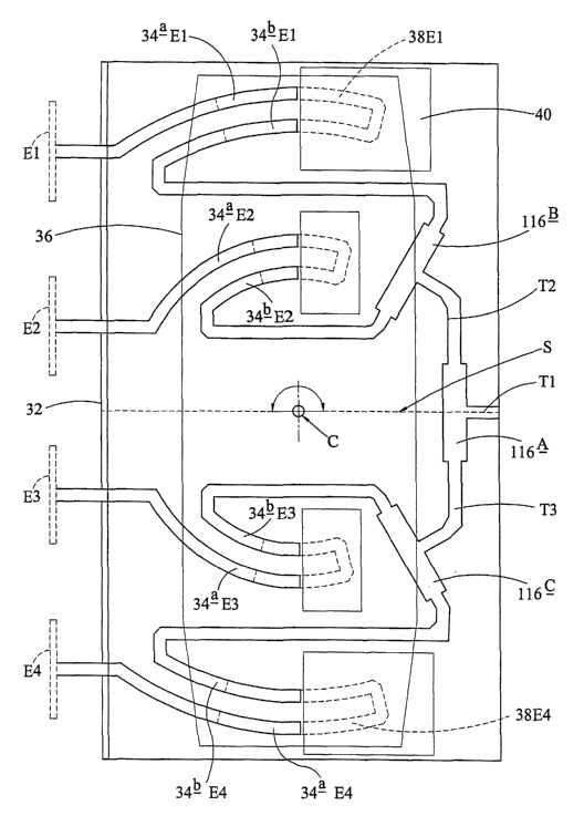
The apparatus also includes a second board 36, shown in outline in Figure 6
but
best illustrated in Figure 7, which is pivotally or rotatably connected to the
first
board 32 at a point C, and is thus pivotal or rotatable about an axis of the
board
32 through point C. The second board 36 has printed or otherwise disposed
thereon four coupling links, each in the form of a respective U- haped track
38E1 -38E4 having arms which are arcuate and generally parallel. The second
coupling link 38E2 is disposed radially inwardly of the first coupling link
38E1
corresponding to the relative positions of the track arrangements of the first
and
second devices on the first board 32. The third and fourth coupling links
38E3,
38E4 are disposed substantially symmetrically about the line of symmetry S
relative to the first and second coupling links 38E1, 38E2.
CA 02461967 2004-03-29
WO 03/036759 PCT/GB02/04748
23
In use, angular movement or rotation of the second board 36 relative to the
first
board 32 about pivot point C causes the coupling links 38E1 - 38E4 on the
second board 36 to capacitively couple, to a greater or lesser extent, with
the
tracks 34a, 34b of the corresponding device on the first board 32, in the
manner
described with reference to the apparatus of Figure 3. The amount or angular
movement of the second board 36 relative to the first board 32 determines how
far each coupling link extends over the respective conductive track and,
hence,
the amount of phase adjustment or delay which is applied to the signals on the
transmission lines to each antenna element. In this manner, the phase of
signals
supplied on the transmission lines to all four of the antenna elements can be
adjusted through movement of a single board 36.
It will be understood that rotation of the second board 36 in, for example, a
clockwise direction with respect to the drawing will increase the effective
length
of the transmission lines connected to the first and second antenna elements
E1,
E2, but will reduce the effective length of the transmission lines connected
to the
elements E3, E4.
Furthermore, the increase in effective length of the transmission line to the
first
element El will be greater than that of the transmission line to the second
element E2 owing to the greater initial length of the conductive tracks 34aE1,
34bE1 in the first device. Similarly, the decrease in effective length of the
transmission line to the fourth element E4 will be greater than that of the
transmission line to the third element E3.
In fact, in order to tilt the antenna whilst retaining maximum boresight gain
and
maximum suppression of the side lobes it is preferable to retain a linear
phase
front over most or all of the tilt range. In the preferred embodiment,
therefore,
delays of T, 2T, 3T and 4T, or relative equivalents thereof, are applied to
the
CA 02461967 2004-03-29
WO 03/036759 PCT/GB02/04748
24
elements El to E4, by the respective phase adjustment device. In practice,
this is
achieved by ensuring that the radial positions of the tracks 34a, 34b of each
device are separated by equal amounts.
In a modification to the apparatus of Figure 6, part of which is illustrated
in
Figure 8, each phase adjustment device has a series arrangement of coupling
links and tracks, as described with reference to Figure 5, in order to
increase the
range of delay which can be applied to signals on the respective transmission
line. In some applications, it may be desirable to have a series arrangement
for
some devices and a single arrangement for other devices. Figure 9 illustrates
the
layout of the coupling links 38a, 38b on the second board 36 for a series
arrangement of a single device.
In an alternative embodiment shown in Figure 10, the signal distribution
network
comprising the splitters 116A, 116B, 116C are disposed on the second board 36
and connection between the antenna port or the splitter unit 116 (depending on
the number of elements in the antenna) and the first splitter unit 116A is via
a
single conductive input track Ti and a capacitive link similar to those used
in the
phase adjustment devices on the first board 32.
Figure 11 illustrates more clearly the arrangement of conductive tracks and
the
splitter units on the second board 36. In this embodiment, each phase
adjustment
device has only a single length of conductive track disposed on the first
board.
32, rather than two parallel tracks as in the previously described
embodiments.
Similarly, the conductive link for each device comprises only a single,
arcuate
length of track rather than a U-shaped section of transmission line.
In use, the coupling link capacitively couples with the respective track in
the
same manner as described previously but, in this embodiment, a lOmm
CA 02461967 2004-03-29
WO 03/036759 PCT/GB02/04748
movement of the second board 36 will produce an effective increase in length
of
the transmission line of lOmm.
Figure 12 illustrates a modification to the apparatus of Figures 10 and 11 in
which each phase adjustment device includes an arrangement of tracks and
coupling links which gives an effective increase in length of the transmission
line
of three times the distance moved by the second board 36. Figure 13
illustrates
the layout of the conductive tracks 38aE1, 38bE2 on the second board 36 for
the
Figure 12 embodiment, said tracks forming the coupling link for a single
device.
Referring now to Figure 14, this illustrates a phased array antenna system
incorporating a number of apparatus according to the invention. -In the
embodiment shown in Figure 14, each apparatus 152E1 to 152E4 is used to
control the phase of signals supplied to two separate antenna elements. Thus
each
apparatus may be broadly similar to the apparatus shown in Figures 6 to 9 but
having conductive track and coupling link arrangements for only two phase
adjustment devices instead of four. The analogy and/or differences between the
apparatus of Figure 14 and the apparatus of Figures 6 to 9 will be fully
understood by those skilled in the art.
In Figure 14, angular movement of the second boards in the phase adjustment
apparatus 152E1 to 152E4 (which are in the form of generally circular discs)
is
achieved by linear movement of an actuating arm 152. The actuating arm 152 is
pivotally and eccentrically mounted to each of the discs in each apparatus. As
in
the embodiment of Figure 2, movement of the actuating arm 152 in the
directions
shown by the arrow A is achieved by means of a servo motor 160 or the like.
The servo motor 160 is again controlled by signals generated by a servo
controller 162 and supplied to the servo motor 160 via a control cable 164 and
a
control port 166. The servo controller 162 may be located remote from the
CA 02461967 2004-03-29
WO 03/036759 PCT/GB02/04748
26
antenna assembly 102, for example in the base-station 104. The base station
104
may be located at the base of the antenna mast, or may be located several
miles
from the antenna mast if preferred.
It will be appreciated that such linear movement will result in the same
angular
movement applied to each disc. In order to retain maximum boresight gain and
control of the side lobe levels, it may be necessary for each antenna element
E1-
E8 to have a different phase shift for a given extent of movement of the
actuating
arm 162. In this case the arrangements of conductive tracks and coupling links
for each device may be slightly different (for example as in Figure 10) in
order
to give the desired relationship between linear movement of the actuating arm
162 and phase shift of signals supplied to the elements.
Figures 15 and 16 show a further embodiment and illustrate how the system of
the present invention can be used with a dual-polarity antenna assembly. The
use
of dual polarity antenna assemblies is well known and common in
telecommunication systems. Figure 15 is a front view of a four element, dual
polarity antenna 702 having crossed dipoles mounted above a reflecting
backplane 704. The axis of rotation of the second board 36 is indicated by the
dashed line X.
In this embodiment, the antenna assembly 702 consists of a stack of crossed
dipole elements, one array of elements E1+ to E4+ angled at +45° to the
vertical and the other array of elements E1- to E4- at -45° to the
vertical. The
arrays for each polarity axe effectively electrically separate with signals
from the
base-station 104 being applied to individual signal distribution networks via
separate input ports 112 (as in Figure 2) to be supplied to each array.
CA 02461967 2004-03-29
WO 03/036759 PCT/GB02/04748
27
Each array is thus provided with a respective separate phase adjustment
apparatus, such as that described above with reference to Figures 6 to 13.
However, both apparatus are adjustable by means of a common servo control
motor, such as that described in relation to Figures 2 and 14, so that both
arrays
have the same angle of electrical tilt.
Figure 15 shows the antenna assembly in plan view. The first phase adjustment
apparatus connected to the antenna elements E1+ to E4+ in the positive
polarity
array comprises an arrangement as illustrated in and described with reference
to
Figures 3 and 4A. Specifically, the apparatus comprises a first board 32+
having
conductive tracks 34a+, 34b+ printed or otherwise disposed thereon, a
dielectric substrate 40+ disposed adjacent to the end of the first board 32+,
and
a second board 36+ having a U-shaped coupling link 38+ printed or otherwise
disposed thereon.
The second phase adjustment apparatus connected to the antenna elements E1- to
E4- in the negative polarity array comprises a similar arrangement to the
first
phase adjustment apparatus, which is mounted "back-to-back" with the first
apparatus via an additional board 146 having a ground plane on each surface.
The purpose of the additional board 146 and ground planes is described with
reference to Figures 4A to 4D.
The second boards 36+, 36- are connected together via, and movable jointly by,
a common shaft coupled to a servo mechanism, such as that described with
reference to Figures 2 and 13. Movement of the second boards may be angular,
as in the embodiments of Figures 6 to 12, or linear, as in the embodiments of
Figures 3 to 5. It will be understood that the embodiments of Figures 3 to 5
may
be extended to include two or more phase adjustment devices so that linear
CA 02461967 2004-03-29
WO 03/036759 PCT/GB02/04748
28
movement of a single, common second board 36 can adjust the phase of signals
on two or more transmission lines.
It will be appreciated that the present invention provides for the independent
phase shifting of individual elements within a phased array antenna system.
The
control of the phase of signals supplied to individual antenna elements allows
an
optimum VRP or beam pattern to be produced with maximum boresight gain and
lower side lobe levels. The performance of such an antenna system is improved
compared with existing systems.
Specifically, the invention provides a number of advantages over existing
systems. For example, the use of a linearly or angularly movable board enables
the correct amount of delay to be applied to the signals supplied to each
antenna
element, thereby to obtain maximum boresight gain and maximum suppression of
the side lobes over the range of tilt angles of the antenna. Furthermore, this
correct phase shift is achieved through movement of only a single antenna
element, thus reducing cost and weight and improving reliability.
In addition, the invention may be implemented using a number of different
constructions, such as micro-strip or tri-plate constructions, depending on
requirements. Finally, the use of one more U-shaped coupling links together
with
the dielectric substrate 40 permits a large increase in effective length of
the
transmission line for a relatively small movement of the second board. The use
of the dielectric substrate is entirely optional, to provide an additional
delay
effect, and can be used with any of the embodiments described above if
desired.
It will be appreciated that the present invention is applicable to an assembly
having any number of antenna elements (at least two) grouped into any number
of sub-arrays, and including an assembly having a number, n, of antenna
CA 02461967 2004-03-29
WO 03/036759 PCT/GB02/04748
29
elements with one antenna element in each sub-array (i.e. n sub-arrays). It
will
also be appreciated that the system described previously is described as a
system
for transmitting signals but, additionally or alternatively, it may be
operated as a
receiver system.
Throughout the specification, a reference to "electrical tilt" shall be taken
to
mean adjustment of the radiation pattern transmitted and/or received from the
antenna assembly without physically moving the antenna radome, or the antenna
elements, but instead implemented by adjusting the phase of signals supplied
to
one or more of the antenna elements. It will be appreciated, however, that
electrical tilt may be adjusted by an arrangement having both mechanical and
electrical adjustment elements, as shown for example in Figure 14.
Furthermore,
for the arrangement in Figure 14, it will be appreciated that the adjustment
of
electrical tilt implemented by the mechanical phase adjustment arrangements
150E1-150E2 or 15~E1-152E2. includes an electrical control means, in the form
of the servo controller 162, such that the combined system may be referred to
as
"a system for adjusting the electrical tilt of an antenna system including a
mechanical adjustment arrangement controlled by electrical means" .
It will be appreciated that, although the antenna system of the present
invention
is described herein in terms of the transmitted VRP, in practice the system
will
preferably be adapted for operation in receive mode, whereby the antenna
elements are arranged to receive signals, and such adaptation would be readily
apparent to a person skilled in the art based on the preceding description.