Note: Descriptions are shown in the official language in which they were submitted.
CA 02462178 2009-11-19
TRANSMITTER PHOTONIC INTEGRATED CIRCUIT (TxPIC) CHIPS
BACKGROUND OF THE INVENTION
Field of the Invention
This invention relates generally to optical telecommunication systems and more
particularly to optical transport networks employed in such systems deploying
photonic
integrated circuits (PICs) for wavelength division multiplexed (WDM) or dense
wavelength
division multiplexed (DWDM) optical networks.
Description of the Related Art
If used throughout this description and the drawings, the following short
terms have the
following meanings unless otherwise stated:
1 R - Re-amplification of the information signal.
2R - Optical signal regeneration that includes signal reshaping as well as
signal
regeneration or re-amplification.
3R - Optical signal regeneration that includes signal retiming as well as
signal reshaping
as well as re-amplification.
4R - Any electronic reconditioning to correct for transmission impairments
other than 3R
processing, such as, but not limited to, FEC encoding, decoding and re-
encoding.
A/D - Add/Drop.
APD - Avalanche Photodiode.
AWG - Arrayed Waveguide Grating.
BER - Bit Error Rate.
CD - Chromatic Dispersion.
CDWM - Cascaded Dielectric wavelength Multiplexer (Demultiplexer).
CoC - Chip on Carrier.
DBR - Distributed Bragg Reflector laser.
EDFAs - Erbium Doped Fiber Amplifiers.
-1-
CA 02462178 2009-11-19
DAWN - Digitally Amplified Wavelength Network.
DCF - Dispersion Compensating Fiber.
DEMUX - Demultiplexer.
DFB - Distributed Feedback laser.
DLM - Digital Line Modulator.
DON - Digital Optical Network as defined and used in this application.
EA - Electro-Absorption.
EAM - Electro-Absorption Modulator.
EDFA - Erbium Doped Fiber Amplifier.
EML - Electro-absorption Modulator/Laser.
EO - Electrical to Optical signal conversion (from the electrical domain into
the optical
domain).
FEC - Forward Error Correction.
GVD - Group Velocity Dispersion comprising CD and/or PMD.
ITU - International Telecommunication Union.
MMI - Multimode Interference combiner.
MPD - Monitoring Photodiode.
MZM - Mach-Zehnder Modulator.
MUX - Multiplexer.
NE - Network Element.
NF - Noise Figure: The ratio of input OSNR to output OSNR.
OADM - Optical Add Drop Multiplexer.
OE - Optical to Electrical signal conversion (from the optical domain into the
electrical
domain).
OEO - Optical to Electrical to Optical signal conversion (from the optical
domain into the
electrical domain with electrical signal regeneration and then converted back
into optical
domain) and also sometimes referred to as SONET regenerators.
OEO-REGEN - OEO signal REGEN using opto-electronic regeneration.
-2-
CA 02462178 2009-11-19
Cr
00 - Optical-Optical for signal re-amplification due to attenuation. EDFAs do
this in
current WDM systems.
000 - Optical to Optical to Optical signal conversion (from the optical domain
and
remaining in the optical domain with optical signal regeneration and then
forwarded in optical
domain).
000-REGEN - 000 signal REGEN using all-optical regeneration.
OSNR - Optical Signal to Noise Ratio.
PIC - Photonic Integrated Circuit.
PIN - p-i-n semiconductor photodiode.
PMD - Polarization Mode Dispersion.
REGEN - digital optical signal regeneration, also referred to as re-mapping,
is signal
restoration, accomplished electronically or optically or a combination of
both, which is
required due to both optical signal degradation or distortion primarily
occurring during optical
signal propagation caused by the nature and quality of the signal itself or
due to optical
impairments incurred on the transport medium.
Rx - Receiver, here in reference to optical channel receivers.
RxPIC - Receiver Photonic Integrated Circuit.
SDH - Synchronous Digital Hierarchy.
SDM - Space Division Multiplexing.
Signal regeneration (regenerating) - Also, rejuvenation. This may entail 1 R,
2R, 3R or 4R
and in a broader sense signal A/D multiplexing, switching, routing, grooming,
wavelength
conversion as discussed, for example, in the book entitled, "Optical Networks"
by Rajiv
Ramaswami and Kumar N. Sivarajan, Second Edition, Morgan Kaufmann Publishers,
2002.
SMF - Single Mode Fiber.
SML - Semiconductor Modulator/Laser.
SOA - Semiconductor Optical Amplifier.
SONET - Synchronous Optical Network.
SSC - Spot Size Converter, sometimes referred to as a mode adapter.
TDM - Time Division Multiplexing.
-3-
CA 02462178 2009-11-19
TEC - Thermo Electric Cooler.
TRxPIC - Monolithic Transceiver Photonic Integrated Circuit.
Tx - Transmitter, here in reference to optical channel transmitters.
TxPIC - Transmitter Photonic Integrated Circuit.
VOA - Variable Optical Attenuator.
WDM - Wavelength Division Multiplexing. As used herein, WDM includes Dense
Wavelength Division Multiplexing (DWDM).
DWDM optical networks are deployed for transporting data in long haul
networks,
metropolitan area networks, and other optical communication applications. In a
DWDM
system, a plurality of different light wavelengths, representing signal
channels, are transported
or propagated along fiber links or along one more optical fibers comprising an
optical span.
In a conventional DWDM system, an optical transmitter is an electrical-to-
optical (EO)
conversion apparatus for generating an integral number of optical channels X1,
X2, XN, where
each channel has a different center or peak wavelength. DWDM optical networks
commonly
have optical transmitter modules that deploy eight or more optical channels,
with some
DWDM optical networks employing 30, 40, 80 or more signal channels. The
optical
transmitter module generally comprises a plurality of discrete optical
devices, such as a
discrete group or array of DFB or DBR laser sources of different wavelengths,
a plurality of
discrete modulators, such as, Mach-Zehnder modulators (MZMs) or electro-
absorption
modulators (EAMs), and an optical combiner, such as a star coupler, a multi-
mode
interference (MMI) combiner, an Echelle grating or an arrayed waveguide
grating (AWG).
All of these optical components are optically coupled to one another as an
array of optical
signal paths coupled to the input of an optical combiner using a multitude of
single mode
fibers (SMFs), each aligned and optically coupled between discrete optical
devices. A
semiconductor modulator/laser (SML) may be integrated on a single chip, which
in the case of
an electro-absorption modulator/laser (EML) is, of course, an EA modulator.
The modulator,
whether an EAM or a MZM, modulates the cw output of the laser source with a
digital data
signal to provide a channel signal which is different in wavelength from each
of the other
channel signals of other EMLs in the transmitter module. While each signal
channel has a
center wavelength (e.g., 1.48 m, 1.52 m, 1.55 m, etc.), each optical
channel is typically
assigned a minimum channel spacing or bandwidth to avoid crosstalk with other
optical
channels. Currently, channel spacings are greater than 50 GHz, with 50 GHz and
100 GHz
being common channel spacings.
-4-
CA 02462178 2009-11-19
An optical fiber span in an optical transport network may provide coupling
between an
optical transmitter terminal and an optical receiver terminal. The terminal
traditionally is a
transceiver capable of generating channel signals as well as receiving channel
signals. The
optical medium may include one or more optical fiber links forming an optical
span with one
or more intermediate optical nodes. The optical receiver receives the optical
channel signals
and converts the channel signals into electrical signals employing an optical-
to-electrical (OE)
conversion apparatus for data recovery. The bit error rate (BER) at the
optical receiver for a
particular optical channel will depend upon the received optical power, the
optical signal-to-
noise ratio (OSNR), non-linear fiber effects of each fiber link, such as
chromatic dispersion
(CD) and polarization mode dispersion (PMD), and whether a forward error
correction (FEC)
code technique was employed in the transmission of the data.
The optical power in each channel is naturally attenuated by the optical fiber
link or spans
over which the channel signals propagate. The signal attenuation, as measured
in dB/km, of
an optical fiber depends upon the particular fiber, with the total loss
increasing with the length
of optical fiber span.
As indicated above, each optical fiber link typically introduces group
velocity dispersion
(GVD) comprising chromatic dispersion (CD) and polarization mode dispersion
(PMD).
Chromatic dispersion of the signal is created by the different frequency
components of the
optical signal travel at different velocities in the fiber. Polarization mode
dispersion (PMD) of
the signal is created due to the delay-time difference between the
orthogonally polarized
modes of the signal light. Thus, GVD can broaden the width of an optical pulse
as it
propagates along an optical fiber. Both attenuation and dispersion effects can
limit the
distance that an optical signal can travel in an optical fiber and still
provide detectable data at
the optical receiver and be received at a desired BER. The dispersion limit
will depend, in
part, on the data rate of the optical channel. Generally, the limiting
dispersion length, L, is
modeled as decreasing inversely with B2, where B is the bit rate.
The landscape of optical transport networks has changed significantly over the
past ten
years. Prior to this time, most long haul telecommunication networks were
generally handled
via electrical domain transmission, such as provided through wire cables,
which is bandwidth
limited. Telecommunication service providers have more recently commercially
deployed
optical transport networks having vastly higher information or data
transmission capability
compared to traditional electrical transport networks. Capacity demands have
increased
significantly with the advent of the Internet. The demand for information
signal capacity
increases dramatically every year.
-5-
CA 02462178 2009-11-19
In a conventional long haul DWDM optical network, erbium doped fiber
amplifiers
(EDFAs) may be employed at intermediate nodes in the optical span to amplify
attenuated
optical channel signals. Dispersion compensation devices may also be employed
to
compensate for the effects of fiber pulse dispersion and reshape the optical
pulses
approximately to their original signal shape.
As previously indicated, a conventional DWDM optical network requires a large
number
of discrete optical components in the optical transmitter and receiver as well
as at intermediate
nodes along the optical link between the transmitter terminal and the receiver
terminal. More
particularly, each optical transmitter typically includes a semiconductor
laser source for each
optical channel. Typically a packaged module may include a semiconductor laser
and a
monitoring photodiode (MPD) to monitor the laser source wavelength and
intensity and a heat
sink or thermal electric cooler (TEC) to control the temperature and,
therefore, wavelength of
the laser source. The laser sources as well as the optical coupling means for
the output light of
the laser source to fiber pigtail, usually involving an optical lens system,
are all mounted on a
substrate, such as a silicon microbench. The output of the laser pigtail is
then coupled to an
external electro-optical modulator, such as a Mach-Zehnder lithium niobate
modulator.
Alternatively, the laser source itself may be directly modulated. Moreover,
different
modulation approaches may be employed to modulate the external modulator, such
as dual
tone frequency techniques.
The output of each modulator is coupled via an optical fiber to an optical
combiner, such
as, an optical multiplexer, for example, a silica-based thin film filter, such
as an array
waveguide grating (AWG) fabricated employing a plurality of silicon dioxide
waveguides
formed in a silica substrate. The fibers attached to each device may be fusion
spliced together
or mechanically coupled. Each of these device/fiber connections introduces a
deleterious,
backward reflection into the transmitter, which can degrade the channel
signals. Each optical
component and fiber coupling also typically introduces an optical insertion
loss.
Part of the cost of the optical transmitter is associated with the requirement
that the optical
components also be optically compatible. For example, semiconductor lasers
typically
produce light output that has a TE optical mode. Conventional optical fibers
typically do not
preserve optical polarization. Thus, optical fiber pigtails and modulators
will transmit and
receive both transverse electric (TE) and transverse magnetic (TM)
polarization modes.
Similarly, the optical combiner is polarization sensitive to both the TE and
TM modes. In
order to attenuate the effects of polarization dispersion, the modulator and
the optical
combiner are, therefore, designed to be polarization insensitive, increasing
their cost.
-6-
CA 02462178 2009-11-19
Alternatively, polarization preserving fibers may be employed for optically
coupling each
laser source to its corresponding modulator and for coupling each modulator to
the optical
combiner. Polarization preserving fibers comprise fibers with a transverse
refractive index
profile designed to preserve the polarization of an optical mode as originally
launched into a
fiber. For example, the fiber core may be provided with an oblong shape, or
may be stressed
by applying a force to the fiber to warp the refractive index of the waveguide
core along a
radial or cross-sectional lateral direction of the fiber, such as a PANDA TM
fiber. However,
polarization preserving fibers are expensive and increase packaging costs
since they require
highly accurate angular alignment of the fiber at each coupling point to an
optical component
in order to preserve the initial polarization of the channel signal.
A conventional optical receiver also requires a plurality of discrete optical
components,
such as an optical demultiplexer or combiner, such as an arrayed waveguide
grating (AWG),
optical fibers, optical amplifiers, and discrete optical detectors as well as
electronic circuit
components for handling the channel signals in the electrical domain. A
conventional optical
amplifier, such as an EDFA, has limited spectral width over which sufficient
gain can be
provided to a plurality of optical signal channels. Consequently, intermediate
OEO nodes will
be required comprising a demultiplexer to separate the optical channel
signals, photodetector
array to provide OE conversion of the optical signals into the electrical
domain, 3R processing
of the electrical channel signals, EO conversion or regeneration of the
processed electrical
signals, via an electro-optic modulator, into optical signals, optical
amplifiers to amplify the
channel signals, dispersion compensators to correct for signal distortion and
dispersion, and an
optical multiplexer to recombine the channel signals for propagation over the
next optical link.
There is considerable interest in DWDM systems to increase both the data rate
of each
signal channel as well as the number of channels, particularly within the gain
bandwidth of the
EDFA. However, increasing the channel data rate necessitates increasing the
number of
intermediate nodes along the optical path to provide the required signal
dispersion
compensation and amplification. Increasing the number of channels requires
precise control
of channel assignment and more precise control over signal dispersion, which
dramatically
increases the complexity and cost of the fiber-optic components of the system.
A further
complication is that many pre-existing optical networks use different types of
optical fibers in
the different optical links of the optical network having, therefore,
different dispersion effects
over different fiber lengths. In some cases, the wavelengths of the optical
channels generated
at the optical transmitter may not be optimal for one or more optical links of
the optical span.
-7-
CA 02462178 2009-11-19
What is desired are improved techniques to provide DWDM optical network
services
through improved, integrated optical network components and systems.
OBJECTS OF THE INVENTION
It is an object of an aspect of this specification to provide an optical
transmitter or
transceiver that comprises a PIC with integrated active and passive components
adapted to
generate and/or receive optical channel signals approximately conforming to a
standardized
wavelength grid, such as the ITU wavelength grid.
It is another object of an aspect of this specification to provide an
integrated optical
component where the optical transmitter, optical receiver or optical
transceiver is an integrated
photonic integrated circuit (PIC).
It is another object of an aspect of this specification to provide a photonic
integrated
circuit (PIC) comprising an array of modulated sources, each providing a
modulated signal
output at a channel wavelength different from the channel wavelength of other
modulated
sources and a wavelength selective combiner having an input optically coupled
to received all
the channel signal outputs from the modulated sources and provide a combined
output signal.
It is a further object of an aspect of this specification to provide an
integrated optical
component where the optical transmitter or optical transceiver comprises an
integrated
photonic integrated circuit (PIC) to eliminate the required optical alignment
and optical
coupling of discrete optical components via optical waveguide devices or
optical fibers.
Another object of an aspect of this specification is the provision of a Tx PIC
chip that
includes multiple signal channels where each channel comprises a modulated
source of
different wavelength where all the wavelengths are approximated to a
standardized
wavelength grid, with their channel signal outputs coupled to an optical
combiner to provide
at its output a combined channel signal.
SUMMARY OF THE INVENTION
According to this invention, a photonic integrated circuit (PIC) chip
comprising an array
of modulated sources, each providing a modulated signal output at a channel
wavelength
different from the channel wavelength of other modulated sources and a
wavelength selective
combiner having an input optically coupled to received all the channel signal
outputs from the
modulated sources and provide a combined output signal on an output waveguide
from the
-8-
CA 02462178 2009-11-19
chip. The modulated sources, combiner and output waveguide are all integrated
on the same
chip.
An optical transmitter comprises a photonic integrated circuit chip or TxPIC
chip having
an integrated array of modulated sources which may be an array of directly
modulated laser
sources or an integrated array of laser sources and electro-optic modulators.
The modulated
sources have their outputs coupled to inputs of an integrated optical
combiner. For example,
the laser array may be DFB lasers or DBR lasers, preferably the former, which,
in one
embodiment may be directly modulated. The electro-optical modulator may be
comprised of
electro-absorption (EA) modulators (EAMs) or Mach-Zehnder modulators (MZMs),
preferably the former. The optical combiner may be a free space combiner or a
wavelength
selective combiner or multiplexer, where examples of the free space combiner
are a power
coupler such as a star coupler and a multi-mode interference (MMI) coupler,
and examples of
a wavelength selective combiner are an Echelle grating or an arrayed waveguide
grating
(AWG), preferably the latter multiplexer because of its lower insertion loss.
This disclosure
discloses many different embodiments of the TxPIC, applications of the TxPIC
in an optical
transport network and wavelength stabilization or monitoring of the TxPIC.
The TxPIC chip in its simplest form comprises a semiconductor laser array, an
electro-
optic modulator array, an optical combiner and an output waveguide. The output
waveguide
may include a spot size converter (SSC) for providing a chip output that is
better match to the
numerical aperture of the optical coupling medium, which is typically an
optical fiber. In
addition, a semiconductor optical amplifier (SOA) array may be included in
various points on
the chip, for example, between the modulator array and the optical combiner;
or between the
laser array and the modulator array. In addition, a photodiode (PD) array may
be included
before the laser array; or between the laser array and the modulator array; or
between an SOA
array, following the laser array, and the modulator array, or between the
modulator array and
the optical combiner; or between an SOA array, following the modulator array,
and the optical
combiner. Also, an SOA may be provided in the output waveguide, preferably a
laser
amplifier, for example, a GC-SOA.
A preferred form of the TxPIC chip may be comprise an array of modulated
sources
comprising a DFB laser array and an EAM array, together with an AWG
multiplexer and
possibly with some on-chip monitoring photodiodes, such as PIN photodiodes or
avalanche
photodiodes (APDs).
-9-
CA 02462178 2009-11-19
Another disclosed feature is a transceiver (TRxPIC) that includes, in addition
to the laser
and modulator arrays and combiner, an array of photodetectors to receive
optical channel
signals for OE conversion as well as provide for transmission of optical
channel signals on
single output waveguide or on separate input and output waveguides. In such an
embodiment,
the optical combiner or multiplexer also functions as an optical decombiner or
demultiplexer.
On-chip optical amplifiers may be provided in the output waveguide from the
optical
combiner or in the input waveguide to the optical combiner to amplify the
channel signals.
Another disclosed feature is deployment of a plurality of output waveguides
from the
TxPIC chip AWG combiner to provide for selection of the output having
optimized passband
characteristics.
Another disclosed feature is the deployment of redundant sets of modulated
sources, such
as, for examples, EMLs, (combination laser/modulator) on the TxPIC chip
coupled to the
optical combiner for substitution of faulty EMLs thereby enhancing chip yield.
Another disclosed feature is the deployment of an on-chip photodiode on the
TxPIC to
monitor or check for antireflection qualities of an AR coating applied to the
front facet of the
TxPIC chip.
Another disclosed feature is the provision of PIC OEO REGEN chip or chips
where the
PIC chip(s) are flip chip mounted to IC circuit chips.
Another disclosed feature is the provision of an integrated array of
monitoring
photodiodes on the TxPIC chip adjacent the back end of the array lasers to
monitor their
optical power and may later be cleaved from the TxPIC chip.
Another disclosed feature is the provision of at least one extra set of
modulated sources,
such as SMLs, along the edges of the TxPIC chip or along the edges of the
wafer containing
the TxPIC die.
Another disclosed feature is the provision of a redundant laser source or
modulated source
on the TxPIC to be substituted for faulty laser sources thereby increasing
chip yield.
Another disclosed feature is a TxPIC chip platform that includes a submount
containing
contact leads from the TxPIC chip to be elevated over and spatially separated
from the TxPIC
chip.
Another disclosed feature is a card probe for checking and testing the
operational integrity
of the TxPIC chips while as die within a wafer.
-10-
CA 02462178 2009-11-19
Another disclosed feature is the provision of TxPIC chip geometry that
substantially
prevents stray light from entering the TxPIC output waveguide thereby
affecting the channel
signal insertion loss.
Another disclosed feature is the provision of at least two TxPIC chips that
each have a first
set of channel wavelengths where one of the chips is temperature tuned to
produce a second
set of channel wavelengths different from the first set of channel wavelengths
so that the two
chips together provide a contiguous set of monotonic increasing or decreasing
channel
transmission wavelengths.
Another disclosed feature is the deployment of a plurality of TxPIC chips each
having an
on-chip WDM channel multiplexer where the WDM combined chip outputs are then
multiplexed or interleaved. A plurality of channel signals with wider on-chip
channel spacing
can be combined into a narrower channel spacing through interleaving of the
WDM combined
channel signals.
Another disclosed feature is the deployment of a plurality of RxPIC chips each
having on-
chip WDM channel demultiplexer where the WDM combined chip inputs are first de-
interleaved into red/blue wavelength channel groups followed by red and blue
wavelength
channel group demultiplexing thereby significantly reducing the number of
optical
connections necessary in a large multi-channel optical transport network.
Another disclosed feature is the provision of a wavelength locking apparatus
for a TxPIC
chip .
Other objects and attainments together with a fuller understanding of the
invention will
become apparent and appreciated by referring to the following description and
claims taken in
conjunction with the accompanying drawings.
BRIEF DESCRIPTION OF THE DRAWINGS
In the drawings wherein like reference symbols refer to like parts.
Fig. I is a schematic block diagram of an example of a single channel in a
TxPIC chip.
Fig. 2 is another schematic block diagram of another example of a single
channel in a
TxPIC chip.
Fig. 3 is another schematic block diagram of a further example of a single
channel in a
TxPIC chip.
-11-
I I
CA 02462178 2009-11-19
Fig. 4 is a cross-sectional view of a first embodiment of a monolithic TxPIC
chip
illustrating a signal channel waveguide through an integrated DFB laser, EAM
modulator and
an optical combiner.
Fig. 5 is a cross-sectional view of a second embodiment of a monolithic TxPIC
chip
illustrating a signal channel waveguide through an integrated DFB laser, EAM
modulator and
an optical combiner.
Fig. 6 is a cross-sectional view of a third embodiment of a monolithic TxPIC
chip
illustrating a signal channel waveguide through an integrated DFB laser, EAM
modulator,
semiconductor optical amplifier (SOA) and an optical combiner.
Fig. 7A is a schematic diagram of the plan view of a monolithic TxPIC adapted
also to
receive data from an optical link.
Fig. 7B is a schematic diagram of a modified version of the monolithic TxPIC
of Fig. 7A.
Fig. 7C is a schematic diagram of a further modified version of the monolithic
TxPIC of
Fig. 7A.
Fig. 8 is a schematic diagram of a plan view of a monolithic TxPIC for
utilizing an on-
chip photodetector to monitor facet reflectivity during the antireflection
(AR) coating process.
Fig. 9 is a schematic diagram of a plan view of a first type of monolithic
transceiver
(TRxPIC) with interleaved optical transmitter and receiver components.
Fig. 10 is a schematic diagram of a side view of a second type of monolithic
transceiver
(TRxPIC) useful for 3R regeneration and flip chip coupled to a submount with
control
electronic semiconductor chip components for operating the TRxPIC.
Fig. 11 is a schematic diagram of a plan view of a monolithic TxPIC with
external
monitoring photodiodes (MPDs) for monitoring the wavelength and/or intensity
of the laser
sources.
Fig. 12 is a schematic diagram of a plan view of a monolithic TxPIC with
detachable
integrated MPDs and heater sources provided for each laser source and the
optional SOAs,
and for the optical combiner.
Fig. 13 is a schematic diagram of a plan view of a monolithic TxPIC with MPD
coupled
between each laser source and electro-optic modulator to monitor the output
intensity and/or
wavelength of each laser source.
-12-
CA 02462178 2009-11-19
Fig. 14 is a schematic diagram of a plan view of a monolithic TxPIC with MPD
coupled
between each electro-optic modulator and the optical combiner to monitor the
output intensity
and/or chirp parameter of each modulator.
Fig. 15 is a schematic diagram of a plan view of a monolithic TxPIC with MPD
coupled to
a tapped portion of the multiplexed signal output of the TxPIC to monitor the
signal channel
intensity and wavelength.
Fig. 16 is a schematic diagram of a plan view of a monolithic TxPICs as-grown
in an InP
wafer.
Fig. 17 is a flowchart of a method for generating calibration data during
manufacture to
store calibrated data in adjusting the bias of the laser sources, modulators
and SOAs, if
present, in the TxPIC and thereafter adjust the wavelength of the channels to
be set at the
predetermined wavelengths after which the SOAs, if present, may be further
adjusted to
provide the appropriate output power.
Fig. 18 is a schematic diagram of a plan view of another embodiment of a TxPIC
chip
where additional SMLs are formed at the edges of the InP wafer or, more
particularly, to the
edges of the TxPIC chip or die in order to maximize chip yield per wafer.
Fig. 19A is a schematic diagram of a plan view of another embodiment of a
TxPIC chip
where additional redundant SML sets are formed between SML sets that are to be
deployed
for signal channel generation on the chip and used to replace inoperative
SMLs, either at the
time of manufacture or later in the field, thereby maximizing chip yield per
wafer.
Fig. 19B is a schematic diagram of a plan view of another embodiment of a
TxPIC chip
where additional redundant laser sources are provided for each signal channel
on the chip so
that if one of the pair of laser sources is inoperative, either at the time of
manufacture or later
in the field, the other source can be placed in operation, thereby maximizing
chip yield per
wafer.
Fig. 20 is a schematic diagram of a plan view of another embodiment of a TxPIC
chip
illustrating one embodiment of the provision of RF conductive lines employed
for modulating
the electro-optic modulators on the chip.
Fig. 20A is a graphic illustration of how the modulators of Fig. 20, or any
other modulator
in other embodiments, are operated via negative bias and peak-to-peak swing.
-13-
CA 02462178 2009-11-19
Fig. 21 is a perspective view of a schematic diagram of the bias contacts and
bonding wire
or tape for electro-optic components and the RF lines and contacts for the
electro-optic
modulators.
Fig. 22 is a schematic side view of a probe card with multiple probes inline
with contact
pad on a TxPIC chip to provide PIC chip testing at the wafer level or after
burn-in for
reliability screening prior to final chip fabrication.
Fig. 23 is flowchart of a method for wafer level testing of laser source
output power using
integrated PDs which may later be rendered optically transparent.
Fig. 24 is a schematic diagram of a plan view of another embodiment of a TxPIC
chip
illustrating the geometric arrangement of optical components to insure that
stray light from the
SML components do not interfere with the output waveguides of the optical
combiner.
Fig. 25 is a schematic diagram of a plan view of another embodiment of a TxPIC
chip
deploying Mach-Zehnder Modulators (MZMs) in the TxPIC chip.
Fig. 26 is a cross-sectional view of an embodiment of a DFB laser source that
may be
deployed in Fig. 25.
Fig. 27 is a cross-sectional view of an embodiment of a Mach-Zehnder Modulator
(MZM)
that may be deployed in Fig. 25.
Fig. 28 is a schematic block diagram of another embodiment of a single channel
in the
TxPIC chip of Fig. 25.
Fig. 29 is a schematic block diagram of a further embodiment of a single
channel in the
TxPIC chip of Fig. 25.
Fig. 30 is a graphic illustration of an example of the absorption of a
modulator verses
wavelength.
Fig. 31 is a cross-sectional view of an example of a band-edge electro-
absorption
modulator (BE-EAM).
Fig. 32 is a diagrammatic side view of multiple TxPICs with the same
wavelength grid
output but having separate TEC control to achieve a wavelength band shift of
one PIC relative
to the other to achieve a separate set of signal signals within the wavelength
grid of the optical
combiner.
Fig. 33 is a representative example of the multiple wavelength outputs of the
pair of
TxPIC chips of Fig. 32.
-14-
CA 02462178 2009-11-19
Fig. 34 is a schematic diagram of a plan view of an embodiment of an optical
transmitter
portion of an optical transport system employing a plurality TxPIC chips with
interleaved
signal channel outputs.
Fig. 34A is a graph illustration of the first and second TxPICs of the optical
transmitter of
Fig. 34 showing their wavelength outputs verse power before interleaving with
a wavelength
grid at a larger spatial separation or pitch.
Fig. 34B is a graph illustration of the first and second TxPICs of the optical
transmitter of
Fig. 34 showing their interleaved wavelength outputs verse power after
interleaving with a
wavelength grid at a smaller spatial separation or pitch.
Fig. 35A is an illustration of one kind of interleaving where the TxPICs such
as shown in
Fig. 34 have on-chip channel spacing of 100 GHz or 200 GHz.
Fig. 35B is an illustration of another kind of interleaving where the TxPICs
such as shown
in Fig. 34 have on-chip channel spacing of 50 GHz.
Fig. 36 is a schematic diagram of a plan view of an embodiment of optical
transport
system employing a plurality TxPIC chips with multiplexed signal channels at
the optical
transmitter launched on a fiber link and received at an optical receiver where
the signal
channels are de-interleaved and demultiplexed to a plurality of RxPIC chips.
Fig. 37 is a schematic diagram of a plan view of a TxPIC chip with a
wavelength locker
system utilizing frequency tone identifying tags for each laser source in the
TxPIC.
Fig. 38 is a graphic illustration of a frequency tone for a laser source in
the TxPIC shown
in Fig. 35.
DETAILED DESCRIPTION OF THE INVENTION
Reference is now made to Figs. IA and IB which illustrate, in block form, an
optical path
on a monolithic TxPIC chip 10 showing plural active and passive optically
coupled and
integrated components. What is shown in diagrammatic form is one channel of
such a chip.
Both Figs. IA and 1B show modulated sources coupled to an optical combiner.
Shown in Fig.
IA is one of an array of sources comprising a directly modulated semiconductor
laser 12
integrated with an optical combiner 16 having an optical output waveguide 18
to take a
combined channel signal off-chip. Shown in Fig. 113 is one of an array of
sources comprising
a semiconductor laser 12 optically coupled to one of an array of modulators
comprising an
electro-optic modulator 14 optically coupled to an input of an optical
combiner 16 with the
-15-
CA 02462178 2009-11-19
output of combiner 16 coupled to an optical output waveguide 18. There are
plural optical
paths on chip 10 of semiconductor laser 12 and electro-optic modulator 14,
also in
combination referred to as an SML, these SMLs respectively coupled to inputs
of optical
combiner 16. This is the basic monolithic, generic structure of a TxPIC chip
10 for use in an
optical transmitter module, also referred to by the applicants herein as a DLM
(digital line
module).
The semiconductor laser 12 may be a DFB laser or a DBR laser. While the later
has a
broader tuning range, the former is more desirable from the standpoint of
forming an array of
DFB lasers 12 that have peak wavelengths, which are created in MOCVD employing
SAG
(selective area growth) techniques to approximate a standardized wavelength
grid, such as the
ITU grid. There has been difficulty in the integration of DFB lasers with an
optical combiner
but the careful deployment of SAG will provide a TxPIC 10 that has the
required wavelength
grid. Thus, the optical SML paths, mentioned in the previous paragraph, are
modulated data
signal channels where the modulated channel signals are respectively on the
standardized grid.
Electro-optic modulators 14 may be EAMs (electro-absorption modulators) or
MZMs (Mach-
Zehnder modulators). Optical combiner 18 may be comprised of a star coupler, a
MMI
coupler, an Echelle grating or an arrayed waveguide grating (AWG). one of an
array of
sources. To be noted is that there is an absence in the art, at least to the
present knowledge of
the inventors herein, of the teaching and disclosure of an array of modulated
sources and
wavelength selective optical multiplexer, e.g., such as an arrayed waveguide
grating (AWG)
or Echelle grating In this disclosure, a wavelength selective multiplexer or
combiner is
defined as one that has less than 1/N insertion loss wherein N is the number
of modulated
sources being multiplexed. One principal reason is that it is difficult to
fabricate, on a
repeated basis, an array of lasers with a wavelength grid that simultaneously
matches the
wavelength grid of the a wavelength selective combiner (e.g., an AWG). The AWG
is
preferred because it can provide a lower loss multiplexing structure.
Additionally, an AWG
may provide a narrow passband for grid wavelengths of lasers such as DFB
lasers.
In Fig. 2, there is shown a further embodiment of a monolithic TxPIC 10 chip.
The TxPIC
chip here is the same as that shown in Fig. lB except there is an additional
active component
in the form of semiconductor optical amplifier (SOA) 20. Due to insertion
losses in the
optical components on the chip 10, particularly at points of their coupling,
an on-chip
amplifier 20 may be included in each EML optical path to boost the output
channel signals
from modulators 14. An advantage of SOAs on TxPIC chips 10 compared to their
deployment on RxPIC chips is the relaxation of the optical signal to noise
ratio (OSNR) on the
-16-
CA 02462178 2009-11-19
TxPIC SOAs compared to their employment in RxPIC SOAs, SOAs deployed on RxPIC
chips are positioned at the input of the chip to enhance the gain of the
incoming multiplexed
channel signal and is dominated by ASE generated from the SOA which can effect
the proper
detection of channel signal outputs. This is not as significant a problem in
TxPIC chips which
renders their usage in TxPIC chips as more acceptable in design freedom. As a
result, the
noise figure design criteria are relaxed in the transmitter side, compared to
the receiver side
and being sufficient for 100 km optical fiber link. Thus, OSNR limited optical
devices can
drive the architecture and this has not been recognized by those skilled in
the art. More details
of RxPIC chips can be found in U.S. patent no. 7,116,851.
It should be noted that the peak wavelengths of the SOAs 20 on a TxPIC chip
10, such as,
for example, SOAs 20 following each modulator 14 of each channel on a N
channel TxPIC
chip 10, should preferably have a peak wavelength slightly longer, such as,
for example, in the
range of 10 nm to 80 nm or preferably in the range of 30 nm to 60 nm, than its
corresponding
semiconductor laser, such as a DFB laser, in order to compensate for band-
filling effects in
SOAs 20, which effectively shifts the gain peak of an SOA 14 to shorter
wavelengths when
the SOA is placed into operation. The amount of wavelength shift depends upon
the designed
bias point of the SOA. A preferred way to accomplish a different peak
wavelength in SOAs
20, compared to its corresponding semiconductor DFB laser, is to change the
size or thickness
of the active region of SOA 20 to change its built-in peak wavelength through
the use of SAG
or, alternatively, through multiple layer regrowths. The use of SAG in
fabrication of chip 10
is discussed in more detail in U.S. patent no. 7.058,246.
Also, attention should be drawn to the optimization of active and active
optical component
spacing relative to substrate thickness to minimize thermal cross-talk between
active optical
components on TxPIC chip 10. Inter-component spacing of active optical
components, such
as DFB lasers 12, modulators 14 and SOAs 20, is, in part, driven by thermal
crosstalk, e.g.,
changes in temperature operation of these components that affect the optical
characteristics of
neighboring active optical components, such as their wavelength or their bias
point.
Therefore, these active optical components should be sufficiently spaced in
order to minimize
thermal crosstalk affecting neighboring component operation. Component
separation also
important with respect to with substrate thickness. Ideally, the thickness of
the substrate
should be kept to a maximum in order to minimize wafer breakage, particularly
in the case of
highly brittle InP wafers, as well as breakage at the chip level during
handling or processing.
On the other hand, the substrate should not be too thick rendering cleaving
yields lower or
resulting in excess heating and thermal crosstalk due to thicker substrates.
As an example, for
-17-
CA 02462178 2009-11-19
a 500 m thick InP substrate, a preferred inter-component separation is in the
range of about
200 m to about 600 m.
Reference is now made to Fig. 3 which shows, in block form, a TXPIC chip 10
similar to
the chip shown in Fig. I except the output waveguide 18A from the optical
combiner includes
in its path an SOA. Thus, the multiplexed channel signals may be on-chip
amplified prior to
their launching on an optical transport medium such as an optical fiber link.
This chip output
amplifier may be preferred as a gain-clamped SOA which is discussed in more
detail in
connection with Fig. 9.
Reference is now made to cross section views of various representative
embodiments of a
TxPIC chip 10. These cross-sectional views are not to scale, particularly in
reference to the
active waveguide core 42 of the disclosed semiconductor chips. Chips 10 are
made from InP
wafers and the layers are epitaxially deposited using an MOCVD reactor and
specifically
comprise DFB lasers 12, EAMs. As seen in the cross-sectional view of Fig. 4,
there is shown
an optical EML path and optical combiner of TxPIC chip 10, comprising an InP
substrate 32,
such as n-InP or InP:Fe, followed by a cladding layer 34, a waveguide layer
36, a spacer layer
38 of n-InP, followed by grating layer 40. Grating layer 40 includes a grating
(not shown) in
the section comprising DFB laser 12, as is well known in the art, having a
periodicity that
provides a peak wavelength on a standardized wavelength grid. Grating layer 40
is followed
by layer 41 of n-InP, multiple quantum well region of wells and barriers
employing a
quaternary (Q) such as InGaAsP or AlInGaAs. These quaternaries are hereinafter
collectively
referred to as "Q". These layer are deposited deploying SAG using a mask to
form the
individual DFB bandgaps of their active regions as well as the bandgaps for
the individual
EAMs 14 so that wavelengths generated by the DFB laser 12 will be transparent
to the
individual EAMs 14. Also, the wavelength of the field of combiner 18 will be
shorter than
that of the EAMs 14. As an example, the longest wavelength for a DFB array may
be 1590
nm, its EAM will have a wavelength of 1520 nm and the field of optical
combiner 18 will
have a wavelength of 1360 nm.
The Q active region 42 and the waveguide core 36 layer extend through all of
the
integrated optical components. If desired, the laser, and the SOA 20, if
present, can be
composed of a different active layer structure than the region of the EAM 14.
In this
embodiment, the Q waveguiding layer 36 provides most of the optical
confinement and
guiding through each section of the chip 10.
-18-
CA 02462178 2009-11-19
The chip 10 is completed with the growth of NID-InP layer 44, cladding layer
46, which is
either n-InP or NID-InP, and contact layer 48 comprising p++-InGaAs. Cladding
layer 46 as
well as its overlying contact layer portion is selectively etch away either
over the EMLs or
over the field of optical combiner 18 and regrown so that the partition
results in p-InP layer
46A and p++-InGaAs layer 48A in regions of DFB lasers 12 and EAMs 14 and a NID-
InP
layer 46B and a passivation layer 48B in region of the field of optical
combiner 18. The
reason for this etch and regrowth is to render the optical combiner field 18
non-absorbing to
the optical channel signals propagating thought this optical passive device.
More is said and
disclosed relative to this matter in U.S. patent no. 7,958,246.
Chip 10 is completed with appropriate contact pads or electrodes, the p-side
electrodes 44
and 46 shown respectively for DFB laser 12 and EAM 14. If substrate 32 is
semiconductive,
i.e., n-InP, then an n-side electrode is provided on the bottom substrate 32.
If substrate 32 is
insulating, i.e., InP:Fe, the electrical contact to the n-side is provided
through a via (not
shown) from the top of the chip down to n-InP layer 34. The use of a semi-
insulating
substrate 32 provides the advantage of minimizing electrical cross-talk
between optical
components, particularly active electrical components in aligned arrays, such
as DFB lasers 12
and EAMs 14. The inter-component spacing between adjacent DFB laser 12 and
EAMs 14 be
about 250 m or more to minimize cross-talk at data rates of 10 Gbit per sec.
Reference is now made to Fig. 5 which is the same as Fig. 4 except that Q
waveguide
layer 36 is epitaxially positioned above active region 42 rather than below
this region as
shown in Fig. 4.
Reference is now made to Fig. 6 which is similar to Fig. 4 except that, in
addition,
discloses an integrated optical amplifier comprising SOA 20 with its p-side
contact pad 49 and
a spot size converter 22 formed in the waveguide 18 from the optical combiner
18. To be
noted is that the selective area growth (SAG) techniques may be employed to
vary the
epitaxial growth rate along the regions of the PIC to vary the thickness of
quantum well active
layers longitudinally along the optical EML paths of these optical active
components. For
example, in the case here, layers 42A in the active region 41 of EAM 14 are
made thinner
compared to the DFB and optical combiner regions so that the optical mode
experiences
tighter confinement during modulation with no probable creation of multi-
modes. Thus on
either side of EAM 14, there are mode adaptors 14X and 14Y formed through SAG
that
respectively slightly tighten the confinement of the optical mode and permit
slight expansion
of the optical mode in the optical combiner where the propagation does become
multi-modal.
-19-
CA 02462178 2009-11-19
In SSC 22 of TxPIC chip 10 of Fig. 6, in region 42B of the active region 42,
the layers
become increasingly narrower so that the optical mode in the case here can
expand more into
NID-InP layer 46B permitting the mode expansion to more approximate the
numerical
aperture of a coupling optical fiber. In this connection, other layers of the
structure may be
shortened, such as in a step-pad manner as is known in the art, to form an
aperture in the
waveguide 18 from the PIC that provides a beam from chip 10 to approximate the
numerical
aperture of a coupling optical fiber.
TxPIC chip 10 is fabricated through employment of MOCVD where, in forming
active
region 42 across all of the chips in an InP wafer, a patterned SiO2 mask is
positioned over the
growth plane of the as-grown InP substrate. The patterned SiO2 mask has a
plurality of
openings of different widths and masking spaces of different widths so that
the growth rates in
the mask openings will depend upon the area (width) of the opening as well the
width of
masks on the sides of the openings. The reason that the mask widths play a
role in what is
deposited in the openings is that the reactants, such as molecules of Ga and
In, in particular In,
breakup or crack from their carrier gas quickly at regions of the SiO2 mask
and will migrate
off the mask into the mask openings. For example, quantum well layers grown in
wider open
areas tend to grow slower and have a different composition than quantum wells
grown on
narrower open areas. This effect may be employed to vary quantum well bandgap
across the
plane of the substrate for each of the DFB lasers 12, EAMs 14 and the field of
the combiner
18. The corresponding differences in quantum well energy can exceed 60 meV,
which is
sufficient to create regions having a low absorption loss at the lasing
wavelength. The SiO2
masks are removed after the growth of active region 42. Additional growth and
a subsequent
etchback and regrowth are then performed, as previously discussed, to form a
continuous
buried waveguide integrated transmitter chip.
An optical transport module may be fabricated employing a separate RxPIC chip
and a
TxPIC chip. However, a TRxPIC chip is employed that includes both transmitter
and receiver
components. The transmitter and receiver components share a common AWG or may
be two
AWGs, a first AWG for the transmitter portion of the TRxPIC and a second AWG
for the
receiver portion of the TRxPIC. In this case, the AWGs may be mirrored imaged
AWGs as
known in the art. Embodiments of TRxPICs 10 are disclosed in Figs. 7A through
8.
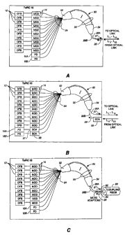
Reference is first made to Fig. 7A illustrating an embodiment of TRxPIC chip
10. Chip
10 comprises an array of DFB lasers 12 and array of EAMs 14 optically coupled
via
waveguides 24 to an optical combiner 18 comprising an arrayed waveguide
grating (AWG)
50. As, an example, TRxPIC may have ten signal channels with wavelengths of 2
to kj o
-20-
CA 02462178 2009-11-19
forming a first wavelength grid matching that of a standardized wavelength
grid. However, as
indicated before, the number of channel signal EMLs may be less than or
greater than ten
channels, the latter depending upon the ability to spatially integrate an
array of EMLs with
minimal cross-talk levels. AWG 50 is an optical combiner of choice because of
its capability
of providing narrow passbands for the respective channel signals thereby
providing the least
amount of noise through its filtering function. Also, AWG 50 provides for
comparative low
insertion loss. AWG 50, as known in the art, comprises an input slab or free
space region 52,
a plurality of grating arms 56 of predetermined increasing length, and an
output slab or free
space region 54. AWG 50 is capable of providing for transmission of
multiplexed channel
signals as well as to receive multiplexed channel signals. In this case, there
are waveguides
26A and 26B coupled between the output slab 54 of AWG 50 and the output of
chip 10.
Output waveguide 26A is the output for multiplexed channel signals 27
generated on-chip by
the EMLs and launched onto the optical link, and input waveguide 26B is the
input for
multiplexed channel signals 29 received from the optical link. To be noted is
that TRxPIC
chip 10 includes an array of integrated photodiodes (PDs) 15, two of which are
shown at 15A
and 15B, for receiving incoming demultiplexed channel signals on optically
coupled
waveguides 24 from AWG 50. Thus, AWG 50 is optically bidirectional and may be
deployed
simultaneously to multiplex outgoing optical channel signals to output
waveguide 26A and to
demultiplex (route) a multiplexed input optical signal, preferably comprising
channel signals
of different wavelengths from the outgoing channel signals, which are coupled
from the
optical link for distribution and detection to PDs 15A, 15B, etc. Thus, AWG 50
can function
in one direction as a multiplexer and in the opposite direction as a
demultiplexer as is known
in the art. PDs 15 may be integrated PIN photodiodes or avalanche photodiodes
(APDs).
There may be, for example, an array of ten such PDs 15 integrated on TRxPIC
10. The
electrical channel signals generated by PDs 15 are taken off-chip for further
processing as
known in the art. It is preferred that the EML inputs from waveguide 24 to
slab 52 of AWG
50 as well as the outputs from slab 52 to PDs 15 are formed in the first order
Brillouin zone
output of slab 52.
Alternatively, it should be noted that the input signal to TRxPIC 10 may be
one or more
service channel signals, for example, from another optical receiver or TRxPIC
transmitter.
AWG 50 would route these signals to appropriate in-chip photodetectors 15 and
taken off-chip
as electrical service signals for further processing.
In the embodiments herein deploying an AWG as an optical combiner, the AWG may
be
designed to be polarization insensitive, although this is not critical to the
design of the TxPIC
-21-
CA 02462178 2009-11-19
10. In general, an AWG does not need to be polarization insensitive because
the propagating
polarization modes from the respective DFB laser sources to the AWG are
principally in the
TE mode. However, due to multimode propagation in the AWG, the TM mode may
develop
in one or more arms of the AWG in a worst case situation. There are ways to
combat this
issue which are to (1) employ polarization selective elements, (2) place a TM
mode filter at
the output of the AWG and/or (3) make the SOAs 20, such as in the case of the
embodiment
of Fig. 6, have the same polarization bias as the DFB lasers 12 so that the
amplification
provided by the SOAs, following modulation, will amplify the TE mode rather
than the TM
mode so that any amount of presence of the TM mode will be substantially
suppressed before
the TE mode encounters the AWG 50.
The design of the passive output waveguide 26A of AWG 50 of TRxPIC chip 10, or
any
chip 10 embodiment output waveguide disclosed herein, involves several
additional
considerations. The total power coupled by the AWG output waveguide 26 into
optical fiber
link should be sufficient to allow low error rate transmission. It is, thus,
desirable that the
output waveguide have a low insertion loss to increase the coupled power.
However, it is also
desirable that the power density in the AWG output waveguide 26 be below the
threshold
limit for two photon absorption. For an AWG output waveguide, such as
waveguide 26, this
corresponds to approximately 20 mW total average power for all channels for a
waveguide
width in the range of approximately I m to 3 m. Additionally, it is also
desirable that
output waveguide 26 be oriented at an angle relative to an axis perpendicular
to the plane of
the output face or facet of chip 10, such as at an angle of about 7 , to
reduce the capture of
stray light emanating from the on-chip EMLs in order to maintain a high
extinction ratio for
signal channels. More will be said about this issue in connection with the
embodiments of
Figs 24A and 24B.
Reference is now made to Fig. 7B which discloses the same TRxPIC 10 of Fig. 7A
except
that the TRxPIC 10 of Fig. 7B includes, in addition, the array of SOAs 58A,
58B, etc. formed
in the on-chip optical waveguides 24 to PDs 15A, 15B, etc. SOAs 58
respectively provide
gain to demultiplexed channel signals that have experienced on-chip insertion
loss through
AWG 50 so that a stronger channel signal is detected by PDs 15. SOAs 58 are
optional and
can be eliminated depending upon the design of AWG 50 where it provides a low
insertion
loss, such as below 3 dB. TRxPIC 10 in both Figs. 7A and 7B include, as an
example, ten
signal channels with wavelengths of X1 to Xto forming a first wavelength grid
matching that of
a standardized wavelength grid. The wavelength grid for received channel
signals may be, for
example, X11 to X20 forming a second wavelength grid matching that of a
standardized
-22-
CA 02462178 2009-11-19
wavelength grid. It is preferred that the incoming channel signals be of
different grid
wavelengths so as not to provide any interference, particularly in AWG 50.
Compare this
embodiment of Fig. 7B with the embodiment shown in Fig. 8 to be later
discussed. In the case
here of Fig. 7B, the wavelengths of the incoming signals are different from
the outgoing
signal, whereas in Fig. 8 the wavelengths of the incoming and outgoing
channels are
interleaved. In either case, the received channels, X11-X20, that are provided
as an output from
the AWG may be coupled into SOAs 58. Furthermore, an optional SOA 59 may be
integrated
in the input waveguide 26B before the input of AWG 50, a shown in Fig. 7B, to
enhance the
incoming multiplexed signal strength prior to demultiplexing at AWG 50.
Reference is now made to Fig. 7C which discloses a TRxPIC 10 that is identical
to that
shown in Fig. 7A except that chip includes integrated mode adaptors or spot
size converters
(SSCs) 62 and 64 respectively in waveguides 26A and 26B at the output of the
chip for
conforming the optical mode of the multiplexed signals from AWG 50 to better
fit the
numerical aperture of optical coupling fiber 60 and for conforming the optical
mode of the
multiplexed signals from fiber 60 to better fit the numerical aperture of chip
10 as well as
waveguide 26B.
Another alternative approach for a TRxPIC 10 is illustrated in Fig. 8, which
is basically
the same as TRxPIC 10 of Fig. 7B except there are less transmitter and
receiver channels, for
example, only six transmitter channels and six receiver channels are
disclosed, and the
integrated receiver channels are interleaved with the integrated transmitter
channels. Also, a
single output waveguide 26 is for both received and transmitted channel
signals for chip 10.
Chip 10 also has a gain-clamped semiconductor optical amplifier (GC-SOA) 70
instead of a
SOA. GC-SOA 70 is preferred, particularly for received channel signal 29, not
only for
providing on-chip gain to these signals but also the gain clamped signal or
laser signal
eliminates the loss of gain to higher wavelength channels. Further, the TE/TM
gain ratio of
the multiplexed signal traversing the GC-SOA 70 is fixed due to the presence
of the gain
clamped signal. Also, GC-SOA 70 provides gain to the outgoing multiplexed
channel signals,
11-110. More about the utility of GC-SOAs is found in U.S. patent no.
7,116,851. A single
AWG 50 is employed for both the transmitter and receiver channels, which
signal channels
have interleaved wavelength bands. The channel wavelength band for the
transmitter
channels are X1-X6, whereas the channel wavelength band for the receiver bands
are Xi+0-
k6+0 where A is a value sufficient to not cause significant cross-talk with
the transmitter
channels. A GC-SOA is required in this embodiment as a non-clamped SOA will
result in
significant cross-talk and pattern dependent effects. Furthermore, it is
likely that the power
-23-
CA 02462178 2009-11-19
levels of the incoming 29 and outgoing 27 channels will be significantly
different resulting in
gain compression of the higher power signals. Thus, a GC-SOA is required for
the practical
implementation of an on-chip amplifier in the location shown in Fig. 8.
Manufacturing variances in waveguide layer thicknesses and grating periodicity
can cause
significant variance in emission wavelength of DFB lasers fabricated on the
same wafer and
substantial lot-to-lot variance. Depending upon the fabrication process
employed, the absolute
accuracy of the DFB/DBR wavelength may be greater than about I nm due to the
empirical
process variances. For a single discrete DFB laser, control of heat-sink
temperature permits
tuning to within less than 0.1 nm. Consequently, it is desirable to monitor
and lock the
emission wavelength of each DFB laser in the array of the TxPIC to its
assigned channel
wavelength while also maintaining the desired output power of each channel.
The light output
of at least one laser may be provided as input to a filter element having a
wavelength-
dependent response, such as an optical transmission filter. The optical output
of the filter is
received by an optical detector. Changes in lasing wavelength will result in a
change in
detected optical power. The lasers are then adjusted (e.g., by changing the
drive current
and/or local temperature) to tune the wavelength. If there are SOAs or PIN
photodiodes on
TxPIC 10 integrated between the DFB lasers and the AWG in each signal channel,
the SOA or
PIN photodiode for each signal channel may be adjusted to adjust the relative
output power
levels to desired levels across the channels.
Reference is made to Fig. 9 illustrating another embodiment, this time of a
TxPIC 10
which comprises only the transmitter channels of EMLs. Each EML optical
channel
comprises a DFB laser 12 and modulator 14 and AWG 50 of Fig. 7A, but having a
single
output waveguide 26 and one single photodiode PD 15T optically coupled by a
waveguide 24
to the input slab 52 of AWG 50. PD 15T may be coupled at the second order
Brillouin zone
of slab 52 rather than the first order Brillouin zone where all the signal
channels are coupled
into slab 52. The application here of PD 15T is different from the previous
embodiments in
that it deployed to check parameters on the chip after manufacture such as the
amount of
reflected light occurring within chip 10. In fabricating a TxPIC chip, it is
often necessary to
AR coat one or more facets of the chip, such as facet IOF of chip 10 where an
AR coating 51
is place on this output facet to prevent facet reflections of light back into
chip 10 from
interfering with the multiplexed output signal. When an AWG 50 is involved,
the second
order Brillouin zone, PD 15T on the input side of AWG 50 may be utilized to
monitor this
reflected light from facet 10F. PD 15T is operated as facet 15T is being AR
coated, i.e., in
situ, or employed as a check of facet coating reflectivity after the AR
coating has been
-24-
CA 02462178 2009-11-19
completed. During in situ use, when a desired, after minimum, reflection is
detected by PD
15, the AR coating process is terminated, the desired thickness of the AR
coating having been
achieved. Also, PD 15T may be deployed later in field use as a trouble
shooting means to
determine if there are any later occurring internal reflections or undesired
light entering the
chip from the optical link interfering with its operation.
As shown in Fig. 10, a TxPIC and a RxPIC are fabricated on a single substrate
with each
having their separate AWGs. In this embodiment, the integrated PICs can be
utilized in a
digital OEO REGEN as also explained and described in U.S. patent no 7,295,783.
In Fig. 10
an OEO REGEN 79 comprises RxPIC 80 and TxPIC 10 integrated as single chip. As
in past
embodiments, TxPIC 10 comprises an array of DFB lasers 12 and EA modulators
14, pairs of
which are referred to as EMLs. The outputs of the EMLs are provided as input
optical
combiner 18, such as, for example an AWG or power (star) coupler. Optical
combiner 18 has
an output at 27 for optical coupling to fiber link. RxPIC 80 comprises an
optical wavelength-
selective combiner 82, such as, for example an AWG or Echelle grating, which
receives an
optical multiplexed signal 29 for demultiplexing into separate wavelength grid
channel signals
which, in turn, are respectively detected at an array of photodetectors 84,
such PIN
photodiodes, providing an array of electrical channel signals.
As noted in Fig. 10, the OEO REGEN 79 is flip-chip solder bonded to a
submount,
including solder bonding at 86 for connecting the converted electrical signals
to IC control
chip or chips 94, via electrical conductors and conductive vias in and on
submount 83. IC
control chip or chips 94 comprise a TIA circuit, an AGC circuit, as known in
the art, and a 3R
functioning circuit for re-amplifying, reshaping and retiming the electrical
channel signals.
The rejuvenated electrical channel signals are then passed through submount,
via electrical
conductors and conductive vias in and on submount, to IC modulator driver 98
where they are
provided to drive EA modulators 14 via solder bonding at 90 via their coupling
through
conductive leads in or on submount 83. Further, IC bias circuit chip 96
provides the bias
points for each of the respective lasers 12 to maintain their desired peak
wavelength as well as
proper bias point for EA modulators 14 midway or along the absorption edge of
the
modulators at a point for proper application the peak-to-peak voltage swing
required for
modulation. As can be seen, the embodiment of Fig. 10 provides for a low cost
digital
regenerator for regeneration of optical channel signals that is compact and
resides almost
entirely in the exclusive form of circuit chips, some electronic and some
photonic. Such an
OEO REGEN 79 is therefore cost competitive as a replacement for inline optical
fiber
amplifiers, such as EDFAs.
-25-
CA 02462178 2009-11-19
To facilitate microwave packaging, the OEO REGEN 79 is preferably flip-chip
mounted
to a submount to form electrical connections to the several IC control chips.
Also, note that
IC control chips can be flip-chip bonded to OEO REGEN 79. Also, further note
that the OEO
REGEN 79 may comprise two chips, one the TxPIC chip 10 and the other the RxPIC
chip 80.
Referring now to Fig. 11, there is shown another embodiment of a TxPIC chip
100A
wherein an array of PDs 101(l) ... 101(N) is provided, separate and outside of
chip 100A,
where each PD 101 is optically coupled to a rear facet of a respective DFB
laser
102(l) ... 102(N). It can be seen that there are an integral number of optical
channels, %I, h, . .
X,,, on chip 100A, each of which has a different center wavelength conforming
to a
predetermined wavelength grid. PDs 101 are included to characterize or monitor
the response
of any or all of respective on-chip DFB lasers 102(1)...102(N). DFB lasers
102(1)...102(N)
have corresponding optical outputs transmitted on corresponding passive
waveguides forming
optical paths that eventually lead to a coupling input of optical combiner
110. For example
shown here, the optical waveguides couple the output of DFB lasers 102(l) ...
102(N,
respectively, to an SOA 104(1)...104(N), which are optional on the chip, an EA
modulator
106(1)...106(N) with associate driver 106A,...106AN, an optional SOA
108(1)...108(N) and
thence optically coupled to optical combiner 110, which may be, for example,
an AWG 50.
Each of these active components 102, 104, 106 and 108 has an appropriate bias
circuit for
their operation. The output waveguide 112 is coupled to an output of optical
combiner 110.
Optical combiner 110 multiplexes the optically modulated signals of different
wavelengths, and provides a combined output signal on waveguide 112 to output
facet 113 of
TxPIC chip 100A for optical coupling to an optical fiber (not shown). SOAs
108(1)...108(N)
may be positioned along optical path after the modulators 106(l) ... 106(N) in
order to amplify
the modulated signals prior to being multiplexed and transmitted over the
fiber coupled to
TxPIC chip 100A. The addition of off-chip PDs 101(l) ... 101(N) may absorb
some of the
power emitted from the back facet of DFB lasers 102(l) ... 102(N), but, of
course does not
directly contribute to insertion losses of light coupled from the front facet
of DFB lasers
102(l) ... 102(N) to other active on-chip components. The utility of off-chip
PDs
101(1)...101(N) is also beneficial for measuring the power of DFB lasers
102(l) ... 102(N)
during a calibration run, and also during its operation, in addition to being
helpful with the
initial testing of TxPIC 100A.
In Fig. 11, cleaved front facet 113 of chip 100A may be AR coated to suppress
deleterious
internal reflections. Where the off-chip PDs 101(l) ... 101(N) are designed to
be integral with
-26-
CA 02462178 2011-01-20
chip 100A, the employment of an AR coating on front facet 113 may be
unnecessary because
much of the interfering stray light internal of the chip comes from the rear
facet of the lasers
reflecting internally to the front facet 113. As will be appreciated by those
skilled in the art,
each DFB laser 102 has an optical cavity providing light in the forward and
rearward
directions.
Conventional semiconductor laser fabrication processes for DFB and DBR lasers
permits
substantial control over laser wavelength by selecting a grating periodicity.
However,
variations in the thickness of semiconductor layers or grating periodicity may
cause some
individual lasers to lase at a wavelength that is significantly off from their
target channel
wavelength. In one approach, each laser and its corresponding SOAs are
selected to permit
substantial control of lasing wavelength (e.g., several nanometers) while
achieving a pre-
selected channel power.
The DFB laser may be a single section laser. Additionally, the DFB laser may
be a multi-
section DFB or DBR laser where some sections are optimized for power and
others to
facilitate wavelength tuning. Multi-section DFB lasers with good tuning
characteristics are
known in the art. For example, multi-section DFB lasers are described in the
paper by
Thomas Koch et al., "Semiconductor Lasers For Coherent Optical Fiber
Communications,"
pp. 274-293, IEEE Journal of Lightwave Technology, Vol. 8(3), March 1990. In a
single or
multi-section DFB laser, the lasing wavelength of the DFB laser is tuned by
varying the
current or currents to the DFB laser, among other techniques.
Alternatively, the DFB laser may have a microstrip heater or other localized
heater to
selectively control the temperature of the laser. In one approach, the entire
TxPIC may be
cooled with a single TEC thermally coupled to the substrate of the TxPIC such
as illustrated
in Fig. 12. Fig. 12 illustrates TxPIC chip IOOB which is substantially
identical to the
embodiment of Fig. I1 except includes, in addition, integrated PDs 107(1)...
(N) between
modulators 106(n)...(N) and SOAs 108(1)...(N), device heaters 102A, 108A and
112 as well
as PDs 101(1)...1O1(N) which, in this case are integrated on chip 100B. PDs
101 may be
deployed for initial characterization of DFB lasers 102 and then subsequently
cleaved away
as indicated by cleave line 116. PDs 107 are deployed to monitor the output
intensity and
modulator parameters such as chirp and extinction ratio (ER).
The array of DFB lasers 102 may have an array bias temperature, TO, and each
laser can
have an individual bias temperature, TO + Ti through the employment of
individual laser
27
CA 02462178 2009-11-19
heaters 102A1...102AN. In Fig. 12, there is shown a heater 102A,...102AN for
each DFB 102
on TxPIC chip 100B, and also a separate heater 111 for optical combiner 110
and a TEC
heater/cooler 114 for the entire the chip. The best combination may be a
heater 102A for each
respective DFB laser 102 and a chip TEC heater/cooler 114, with no heater 111
provided for
combiner 110. In this just mentioned approach, the TEC 114 may be employed to
spectrally
adjust the combiner wavelength grid or envelope, and individual heaters 102A
of DFB lasers
102 are then each spectrally adjusted to line their respective wavelengths to
the proper
wavelength channels as well as to match the combiner wavelength grid. Heaters
102A for
respective DFB lasers 102 may be comprised of a buried heater layer in
proximity to the
periodic grating of each DFB laser, embodiments of which are disclosed and
described in U.S.
patent no. 7,079,715. It should be noted that in employing a chip TEC 114 in
combination
with individual heaters 102A for DFB laser 102, it is preferred that TEC 114
function as a
primary cooler for chip 100B be a cooler, rather than heater, so that the
overall heat
dissipation from chip 100E may be ultimately lower than compared to the case
where TEC
114 is utilized as a heater to functionally tune the combiner wavelength grid.
Where TEC 114
functions primarily as a cooler, a spatial heater 11 may be suitable for
tuning the wavelength
grid of combiner while TEC 114 function as a primary cooler for chip 100B to
maintain a high
level of heat dissipation. Then, individual DFB lasers 102 may be tuned to
their peak
operating wavelengths and tuned to the combiner grid.
Reference is now made to the embodiment of Fig. 13 illustrating TxPIC chip
1000 that is
identical to chip I00A in Fig. 11 except for heaters 102, the addition of
integrated PDs
105(l) ... 105(N) positioned in EML optical paths between SOAs 104(1)...104(N)
and
modulators 106(l) ... 106(N). SOAs 104 are disposed between DFB lasers 102 and
modulators
106 and PDs 105 are disposed between SOAs 104 and modulators 106. In order to
obtain the
desired total output power from DFB lasers 102, two alternatives are now
described. First,
initialization of lasers 102, a bias voltage is applied to PDs 105 for
purposes of monitoring the
output of the DFB lasers 102, attenuation, ab;as, of the photodiodes may,
themselves, result in
an insertion loss. However, by adjusting the bias of SOAs 104, the total
desired output power
for a given EML stage of TxPIC chip 1000 may be maintained. One benefit of PDs
105 is the
provision of dynamic on-chip feedback without necessarily requiring pre-
existing calibration
data. Another benefit of PDs 105 is the enablement of the gain characteristics
of SOAs 104 to
be discerned. Second, during normal operation of TxPIC chip 1000, PDs 105 can
function as
passive components through the lack of any biasing, which, if bias existed,
would provide
some attenuation, ab;m. When PDs 105 function more like a passive device,
e.g., with no
-28-
CA 02462178 2009-11-19
applied reverse bias, insertion losses associated with such in-line PDs 105
may be
substantially eliminated. For many power monitoring application, PDs 105 need
not to be
operated as a reverse biased device and can even be slightly or partially
positive bias to
minimize any residual insertion loss and render them more transparent to the
light from DFB
lasers 102. Alternatively, a small portion, such as 1 % or 2%, of the light in
the EML optical
path may be tapped off by deploying PDs 105 that include a blazed grating in
the
active/waveguide core, where the light is taken off-chip for other functions
such as
wavelength locking of lasers 102 or adjustment of the laser intensity. As in
the previous
embodiment of Figs. 11 and 12, PDs 105 may be a PIN photodiode or an avalanche
photodiode, where the former is preferred.
Thus, from the foregoing, it can be seen that during a test mode, prior to
cleaving chip
1000 from its wafer, PDs in Fig. 13 may operate as an in-line power taps of
optical power
from DFB lasers 102 to calibrate their operating characteristics. As
previously indicated, after
TxPIC chip IOOC has been cleaved from its wafer, during its a normal
operational mode, PDs
105 may be operated to be optically transparent in order to minimize their
inline insertion
losses, or may be slightly forward biased to further minimize any residual
insertion losses or
may be operated with selected reverse bias to adjust attenuation to a desired
level.
Reference is now made to the embodiment of Fig. 14 illustrating TxPIC chip
I00D, which
is identical to Fig. 12, except there are PDs 109 following SOAs 108 in the
optical paths,
whereas in Fig. 12 PDs 107 precede SOAs 108. PDs 109 are beneficial for
characterizing the
total performance of all optical components upstream of these PDs, and hence,
can be
deployed as monitors of the total channel power before combiner 110.
Furthermore, the
insertion loss of optical combiner can be characterized by utilizing PDs 105
in combination
with an additional photodiode integrated on chip 100D in a higher order
Brillouin zone output
of combiner 110 or positioned in the off-chip output 120 of optical combiner
120, as shown in
Fig. 15.
Reference now is made to Fig. 15 illustrating TxPIC 100E, which is identical
to TxPIC
100B in Fig. 12 except that there is shown a fiber output 120 optically
coupled to receive the
multiplexed channel signals from output waveguide 26 where a portion of the
signals are
tapped off fiber 120 via tap 122 and received by PD 124. PD 124 may be a PIN
photodiode
or an avalanche photodiode. As previously indicated, PD 124 may be integrated
in wafer. PD
124, as employed on-chip, may be employed for testing the chip output prior to
cleaving
TxPIC chip 100E from its wafer, in which case the photodiode is relatively
inexpensive to
fabricate and would be non-operational or cleaved from the chip after use. PD
124 is coupled
-29-
CA 02462178 2009-11-19
to receive a percentage, such as 1% or 2%, of the entire optical combiner
output, permitting
the optical power characteristics of TxPIC chip 100E to be determined during
wafer level
testing, such as for the purposes of stabilization of laser wavelengths and/or
tuning of the
wavelength grid response of optical combiner 110 to reduce insertion losses.
It should be noted that both SOAs, such as SOAs 108, or photodetectors, such
as
photodiodes 109, can further serve as optical modulators or as variable
optical attenuators, in
addition to their roles as monitors. Multiple of these functions can be
performed
simultaneously by a single photodetector, such as photodiode 124, or an
integrated, on-chip
photodiode at a first or higher order output of the multiplexer, or the
functions can be
distributed among multiple photodetectors. On-chip photodetectors can vary
power by
changing insertion loss and, therefore, act as in-line optical circuit
attenuators. They also can
be modulated at frequencies substantially transparent to the signal channel
wavelength grid
with little effect to modulate data that is not necessarily the customer's or
service provider's
data.
Additionally, optical combiner 110 may include integrated photodiodes at the
output of
optical combiner 110 to facilitate in locking the laser wavelengths and/or
tuning of the grid of
optical combiner 110 to reduce insertion losses. Additionally, PD 124 may be
utilized to
determine the high-frequency characteristics of modulators 106. In particular,
PD 124 and
associated electronic circuitry may be employed to determine a bias voltage
and modulation
voltage swing, i.e., the peak-to-peak voltage, required to achieve a desired
modulator
extinction ratio (ER) and chirp as well as to characterize the eye response of
each modulator
through application of test signals to each of the EA modulators 106. The bias
voltage and
voltage swing of the modulator may be varied. An advantage of having PD 124
integrated on
chip 100E is that, after initial optical component characterization, the
photodetector may be
discarded by being cleaved off TxPIC chip 100E. An arrangement where
photodiodes are in
integrated at the output of combiner 110 on TxPIC chip is disclosed in Fig. 7
of U.S. patent
patent no. 7,079,715. The ability to discard the photodetector has the benefit
in that the final,
packaged device does not include the insertion loss of the photodetector
formerly employed to
characterize the performance of the modulator during an initial
characterization step.
Although particular configurations of SOAs and PDs are shown in Figs. 11-15,
it will be
understood by those skilled in the art that more than one SOA may also be
employed along
any channel.
-30-
CA 02462178 2009-11-19
Referring now to Fig. 16, there is shown in-wafer, the chip die of TxPIC 100B,
although
other embodiments of Figs. 12 or 13-15 may be shown. A combination of
photodiodes, both
those inline with EML channels, such as PDs 101 and 109, as well as those off-
line, not
shown, which may be used to tap off optical power from an inline blazed
grating PD or from
tap off from output 112.. Photodiodes may be located in several locations in
TxPICs 100E in
order to perform either on-substrate testing or inline testing when TxPICs
100E is operating
"on-the-fly". Also, a probe tester can be utilized for testing the TxPICs. It
should be noted
that PDs 101 at the rear facet of DFB lasers 102 may be left on the final
cleaved TxPIC chip
and utilized during its operational phase to set, monitor and maintain the DFB
and SOA bias
requirements.
Fig. 17 discloses, in flowchart form, a procedure for adjustment of the
wavelength of the
channel lasers, set to a predetermined grid wavelength, after which the on-
chip SOAs may be
adjusted to provide final appropriate output power. As seen in Fig. 17, first,
a channel is
selected at 130 in the TxPIC for testing. Next, the selected DFB laser is
turned on and the
output is checked via a photodiode, such as PDs 105 in Fig. 13, to generate
data and provide
calibrated data (134) as to whether the laser wavelength is off from its
desired grid wavelength
and by how much. This calibrated data is used to adjust the laser wavelength
(136) by current
or heater tuning. If the desired wavelength is not achieved (138), the
calibration process is
repeated. The change in wavelength may also change the optical power available
since the
power via applied current to the laser affects the amount of power. If
optimized wavelength
and optical power adjustment is achieved (138), then SOA, such as SOAs 104, is
adjusted
(140) to provide to desired output power for the laser. If all of the laser
channels on the
TxPIC chip have not been tested (142), the next laser channel is selected
(146) and the process
is repeated at 132. When the laser channel has been tested, the calibration
data for all laser
channels for the test TxPIC chip is stored at 144 for future use, such as for
recalibration when
the transmitter module in which the TxPIC chip is deployed is installed in the
field. The
stored data functions as benchmark from which further laser wavelength tuning
and
stabilization is achieved.
Reference is now made to Fig. 18 illustrating another configuration for TxPIC
10
deploying dummy optical components to the edges of a wafer and/or edges of the
PIC chips in
order to maximize chip yield. These dummy components would be fabricated in
the same
way as the other optical components on the wafer using MOCVD. TxPIC 10 of Fig.
18
comprises a plurality of DFB lasers 12 and EA modulators 14 formed as
integrated EML
channels which are coupled to AWG 50 via integrated waveguides 24. On adjacent
sides of
-31-
CA 02462178 2009-11-19
these optical components are additional DFB lasers 12A and EA modulators 12A
on one side
and additional DFB lasers 12B and EA modulators 12B on the other side. These
additional
optical components are all shown as optically coupled to AWG 50. However, they
need not
be so connected to AWG 50. Furthermore, it is not necessary that bonding pads
be connected
to them. This will save chip space or chip real estate. The function of the
dummy optical
components is to take on the faulty attributes that occur to fabricate optical
components at
edges of wafers or chips. It is problematic that the areas of component
defects due to wafer
fabrication, such as growth and regrowth steps, lithography, and other
processing steps will
likely be at the edges of the wafer or boarder components on TxPIC chip edges
where these
extra dummy optical components reside. By employing these dummy components,
the yield
of useable wafers and good TxPIC chips will significantly increased.
Generally speaking from MOCVD fabrication experience as well as from backend
chip
processing experience, the component yield on any PIC chip with multiple
optical components
tends to decrease relative to either optical PIC chips formed at the edges of
the wafer or
optical components formed along the edges of the PIC chip. There are several
reasons for this
attribute. First, at the InP wafer level, an outer perimeter region of the
wafer tends to have the
greatest material non-uniformity and fabrication variances. An edge region of
a PIC may
correspond to one of the perimeter regions of the wafer and, hence, also have
such significant
variances. Second, the cleaving of the wafer produces the PIC dies. The
cleaving process
may adversely affect the edge optical components of the PIC die or these edge
components
may experience the greatest amount of handling.
Statistical methods are employed to form a map of edge regions having a
reduced yield
compared with a central region of a chip or die, or at the wafer level. The
redundancy number
of dummy optical components required in an edge region is selected to achieve
a high yield of
wafers where at least one of the dummy optical components is operable for
testing or
replacement of another failed component. As an illustrative example, if the
yield in a central
PIC region was 90% but dropped to 60% in an edge region, each dummy optical
component in
the edge region could include one or more redundant optical components to
increase the
effective dummy optical component yield to be at least comparable to the
central region. It
will also be understood that placing dummy optical components in edge regions
may be
practiced in connection with previously described embodiments.
To be noted is that the output waveguides 26 of AWG 50 in Fig. 18 is a vernier
output in
the first order Brillouin zone output of AWG 50. The optimum waveguide among
the several
-32-
CA 02462178 2009-11-19
waveguides shown is chosen based upon the waveguide exhibiting the best
overall wavelength
grid response.
It should be noted that with respect to the foregoing TxPIC chip and TRxPIC
chip
embodiments as well as, provision should be made for circumvention of free
carrier
absorption due to two photon absorption in passive waveguides 26 from AWG 50.
The output
waveguide length from the optical combiner or AWG must allow sufficient output
power to
permit low error rate transmission but also must be below the limit for 2
photon absorption.
The 2 photon absorption limit is about 20 mW total average power for all
signal channels for
an approximately I m to 3 m wide output waveguide.
Two photon absorption can occur in passive waveguide structures, particularly
if
sufficiently long to induce photon absorption in their waveguide core. There
are several ways
to circumvent this problem. First, reduce the peak intensity in the waveguide,
either
transversely or laterally or both. By rendering the mode to be less confined,
i.e., making the
mode larger, the chance for the onset for two photon absorption will be
significantly reduced
if not eliminated. Second, the peak intensity of the optical mode may be
shifted so as not to
be symmetric within the center of the waveguide, i.e., the peak intensity of
the mode is
asymmetric with respect to the cladding or confining layers of the guide as
well as the center
position of the waveguide core. This asymmetry can be built into the chip
during its growth
process. Third, increase the Eg of core waveguides/cladding layers. In all
these cases, the
point is to reduce the peak intensity in some manner so that the threshold for
two photon
absorption is not readily achieved.
Another approach to reduce or otherwise eliminate the free carrier absorption
due to two
photon absorption is by hydrogenation of the waveguides in situ in an MOCVD
reactor or in a
separate oven. The process includes employing AsH3, PH3 and/or H2 which
creates H+ atom
sites in the waveguide layer material during component fabrication which
dissipate or rid the
waveguide of these absorption carriers.
Reference is now made to Fig. 19A illustrating another embodiment of TxPIC,
which in
the case here includes an extra or dummy EML signal channel beside each of the
EML signal
channels to be deployed for on-chip operation. As shown, extra DFB lasers 12EX
and EA
modulators 14EX are formed on chip 10 adjacent to a corresponding laser 12 and
modulator
14 These sets of such lasers and modulators have the same bandgap wavelengths
and lasing
wavelengths. Thus, if a laser 12 or modulator 14 in an operating set would
fail, the adjacent
laser 12EX and modulator 14EX would be substituted in place of the failed EML
channel set.
-33-
CA 02462178 2009-11-19
Alternatively, it should be realized that, instead of functioning as
replacement EML channel
sets on chip 10, these extra EML channel sets can be deployed later, at an
additional cost to
the carrier provider, to further increase the signal channel capacity of the
transmitter module.
It should be realized that chip 10 can be made to include additional capacity
not initially
required by the service provider at a minimal cost of providing addition
integrated EML
channel sets on the chip which can be placed into operation at a later time.
This is an
important feature, i.e., the utilization of micro-PICs having multiple arrays
of EMLs
fabricated on the same chip.
Reference is now made to Fig. 19B illustrating TxPIC chip 10 with pairs of DFB
lasers
12A and 12B for each EML channel to provide redundancy on TxPIC chip 10. Each
of the
lasers 12A and 12B are coupled to an integrated optical 2x1 combiner 13. Thus,
the second
DFB laser of each pair 12A and 12B, can be placed into operation when the
other DFB laser
fails to meet required specifications or is inoperative. This redundancy can
be applied to
modulators 14 as well. This feature can be combined with the dummy optical
component
feature set forth in Fig. 19A.
Reference is now directed to the TxPIC chip 10 in Fig. 20 which illustrates an
embodiment of the contact layout strategy for EMLs on the chip. A multichannel
TxPIC chip
10 has a substantial area compared to a conventional single semiconductor
laser. Each optical
signal source of a TxPIC requires driving at least one modulator section. Each
modulator
section requires a significant contact pad area for making contact to a
microwave feed. This
creates potential fabrication and packaging problems in routing microwave
feeds across the
substrate onto the modulator contact pads. As illustrated in the embodiment of
TxPIC chip 10
in Fig. 20, as an example, the location of contact pads 171 for the modulators
may be
staggered to facilitate microwave packaging. Microwave contact pads 171 are
coupled to
modulators 14 for coupling RF signals to the modulator electrodes. Chip 10 is
shown with
eight EML channels optically coupled to optical combiner 16 for multiplexing
the channel
signals and placement on output waveguide 18 for coupling to an optical link.
The important
feature is that the EA modulators 14 are staggered relative to one another
along the optical
path between respective DFB lasers 12 and optical combiner 16. The purpose for
this
arrangement is to provide for easier electrical contact directly to the
modulators 14 for signal
modulation and bias. As shown in Fig. 20, co-planar microwave striplines 170,
172 and 174
are fabricated on top of the chip to each modulator 14 from contacts 171,
where lead 170 is
connected to a prepared opening to p-contact 173 and coplanar leads 172 and
174 are
connected to a prepared opening to common n-contact 175. Contacts 175 are
connected to the
-34-
CA 02462178 2009-11-19
n-side of the modulator through a contact via provided in the chip, such as
down to n-InP
layer 38 in the embodiment of Fig. 6. The p-contact pad is connected to the
contact layer,
such as to contact layer 48 in the embodiment of Fig. 6. The modulators 14 are
electrically
separated from one another through etched channels prepared between the
modulators which
may extend down as far as the InP substrate 32 as shown in the embodiment of
Fig. 6. Also, a
bias lead (not shown) is connected to the n and p contacts to provide a bias
midpoint for the
voltage swing from peak-to-peak in modulation of the modulator. Also, bias
leads 176 are
also provided to each of DFB lasers 12 from edge contact pads 170 provided
along the rear
edge of chip 10. Thus, contact pads 171 for modulators 14 are provided along
two side edges
of chip 10 whereas contact pads 1070 are provided along one rear edge of chip
10 for bias
connection to DFB lasers 12 except that the centrally located modulators 14
have their RF and
bias contacts extend from the rear edge contacts 170.
Pad staggering can also be accomplished in several different ways. First,
additional
passive waveguide sections are included to stagger the locations of the
optical modulators
relative to a die or chip edge. For example, a curved passive waveguide
section can be
included in every other DFB laser to offset the location of the optical
modulator and its
contact pads. Second, the contact pads of modulator 14 are geometrically
positioned relative
to the chip edges to be staggered so that straight leads can be easily
designed to extend from
edge contact pads to the staggered modulator pads.
Reference is made to Fig. 20A which illustrates in graphic form the general
waveforms for
modulation of modulators 14. In Fig. 20, there is line 180 which is zero bias.
Modulators 14
are modulated with a negative bias to provide low chirp with high extinction
ratio. Thus, the
voltage bias, VB, is set at a negative bias at 182 and the voltage swing has a
peak-to-peak
voltage, Vpp, 184 within the negative bias range. The modulation of modulator
14 according
to a data signal illustrates the corresponding modulator output at 186. One
specific example
of voltages VB and Vpp is a bias voltage of VB = -2.5V and a swing voltage of
2.5V or Vpp = -
1.25V to -3.75V.
Reference is now made to the embodiment shown in Fig. 21 which is a
perspective view
of a TxPIC chip 10. The assembly in Fig. 21 comprises a multi-layer ceramic,
or similar
submount is utilized. As will be seen in the description of this embodiment, a
submount is
mounted above TxPIC chip 10 and in close proximity to the high-speed
modulation pads on
TxPIC chip 10. Transmission lines are formed on the submount. Microwave
shielding may
be included above the submount. In order to ensure that sufficient isolation
is achieved
-35-
CA 02462178 2009-11-19
between TxPIC 10 and the submount, an airgap, d, is formed between these two
components,
preferably where d is in a range of values around 5 mils or 127 m.
Each of the optical modulators 14 of TxPIC chip 10 require at least one
microwave drive
signal 200 and at least one common stripline 198. However, in the embodiment
here, two
common striplines 198 are utilized to reduce crosstalk between the striplines
of adjacent
striplines to be connected to adjacent modulators 14 on chip 10. RF
striplines, comprising
striplines 198 and 200, are formed on an array connector substrate 195, which
may be made of
a ceramic material, which is spaced, such as by 50 m, from TxPIC chip 10 as
seen at 193.
The forward ends of striplines 198 and 200 are respectively contacted to p-
contact pads 173
and common n-contact pads 175 by means of bonding wires 196B as shown in Fig.
21.
Alternatively, these connections can be made by wire ribbon bonding or with a
flexible circuit
cable.
Chip 10 is supported on CoC submount 190 which includes patterned conductive
leads
191 formed on a portion of the submount 190. These leads may, for example, be
comprised of
TiW/Au. Submount 190 may, for example, be comprised of AIN. These patterned
leads 191
end at contact pads 191A along the rear edge of chip 10. The bias signals
provided on these
leads 191 are transferred to on-chip contact pads 12PD (which may have a 100
m pitch on
TxPIC 10) by means of a wire bonded ribbon 196A, or alternatively, a flexible
circuit cable,
where the respective ribbon leads are connected at one end to contact pads
191A and at the
other end to contact pads 191B for DFB lasers 12. The additional patterned
leads are utilized
for connecting to on-chip laser source heaters and on-chip monitoring
photodiodes.
An important feature of the embodiment of Fig. 21 is the deployment of an L-
shaped
substrate 192 that has a thickness greater than that of chip 10 so that the
mounting of array
connector substrate 195 on the top of L-shaped substrate 192 will provide for
the micro-
spacing of around 5 mils or 127 m between chip 10 and substrate 195 so that
no damage will
occur to chip 10, particularly during the backend processing of connecting
conductor leads to
chip 10. Thus, substrate 192 may be cantilevered over chip 10 or a support
post may be
provided between substrate 192 and substrate 195 at corner 199.
The assembly in the embodiment of Fig. 21 is concluded with top cover 194 over
substrate
195 which is micro-spaced from the top of substrate 195 with spacer substrates
195A and
195B to provide spacing over RF striplines 197. Cover 194 may be made of AIN
or alumina
and is provided for a microwave protection shield for the micro-striplines 198
and 200 as well
as to provide structural support, particularly the suspended portion of the
assembly platform
-36-
CA 02462178 2009-11-19
(comprising parts 195, 19X and 194) overhanging TxPIC chip 10 at 199. Cover
194 also
includes cutout regions 194A and 194B where cutout region 194B provides for
tool access to
make the appropriate contacts 196B of the forward end striplines 198 and 200
respectively to
contact pads 175 and 173 of chip modulators 14. The rearward ends of
striplines 198 and 200
are exposed by cutout region 194A for off-chip assembly connection to a signal
driver circuit
as known in the art.
A conventional alternative to the deployment microwave striplines 197 is to
use wire
bonding. However, it is not practical to use conventional wirebonds to route a
large number
of microwave signals in a PIC. This is due, in part, to the comparatively
large area of the PIC
that would be required to accommodate all the wirebond pads and the wirebonds
would have
to traverse a distance as long as several millimeters to reach all of the
modulators. Also, the
length of such wirebonds would create an excessively large wire inductance
and, therefore,
would not be feasible. Additionally, the microwave cross-talk between the
bonding wires
would be excessive. The high speed application required by TxPIC 10 for higher
speed data
rates requires a transmission line with impedance matching to the drive
circuit which is
difficult if not impossible to achieve with wire bonding. Thus, it is more
suitable to deploy a
flexible circuit microwave interconnect, such as at 196A, to couple RF or
microwave
striplines 197 formed on substrate 195 to contact pads 173 and 175 of each
modulator 14. A
flexible microwave interconnect is an alternative to wirebonds 196A for two
reasons. First,
they provide a reduction in assembly complexity. Second, they provide reduced
inductance
for wirebonds of equivalent length. A flexible circuit microwave interconnect
is a microwave
transmission line fabricated on a flexible membrane, e.g., two traces spaced
apart to form a
co-planar microwave waveguide on a flexible membrane, that is at least one
ground stripline
for each signal stripline. However, in the embodiment of Fig. 21, two ground
striplines are
shown which provides for less signal interference due to crosstalk with other
tri-coplanar
striplines. Each flexible microwave interconnect at 196B would preferably have
a contact
portion at its end for bonding to contact pads 173 and 175 of a modulator 14
using
conventional bonding techniques, such as solder bonding, thermo-compression
bonding,
thermal-sonic bonding, ultra-sonic bonding or TAB consistent with wire ribbon
bonding
and/or flexible cable interconnects.
It should be realized that TxPIC 10 may be flip chip mounted to a submount,
such as an
alumina, aluminum nitride (AIN), or a beryllium oxide (BeO) submount. The
submount is
provided with patterned contact pads. In one approach, the submount includes
vias and
microwave waveguides for providing the signals to the modulators. Conventional
flip chip
-37-
CA 02462178 2011-01-20
soldering techniques are employed to mount the PIC electrical pads to the
submount. The
solder is preferably a solder commonly used for lasers, such as gold tin, or
leas]-tin. A gold-
gold thermo-compression bonding process may also be employed. General
background
information on flip-chip packaging technology is described in the book by Lau,
et al.,
Electronic Packaging: Design, Materials, Process, and Reliability, McGraw
Hill, NY (1998).
Some background information on microwave circuit interconnect technology is
described in
the book by Pozar, Microwave Engineering, John Wiley & Sons, Inc. NY (1998).
There is a significant packaging cost associated with providing separate DC
contact
pads for driving each semiconductor laser, such as DFB lasers or DBR lasers.
Driving the
contact pads of groups of semiconductor lasers simultaneously reduces the
number of DC pin
outs and DC interconnect paths required, which permits a substantial reduction
in PIC area
and packaging complexity, reducing PIC costs. As an example of one approach,
all of the
DFB lasers 12 on a TxPIC 1.0 are driven in parallel. Alternatively, groups of
lasers, e.g., three
lasers, are coupled in parallel. For multi-section lasers having a primary
drive section and a
tuning section, the drive sections of groups of lasers may be driven in
parallel. Driving lasers
in parallel reduces the packaging cost and the number of DC pin outs required.
However, it
also requires that the lasers have a low incidence of electrical short
defects, Moreover, in
embodiments in which groups of lasers are driven in parallel, it is desirable
that the lasers
have similar threshold currents, quantum efficiencies, threshold voltages, and
series
resistances. Alternatively, the lasers may be driven in parallel, as described
above with the
current to each laser being tuned by trimming a resistive element couple in
the electrical drive
line to the laser. Such trimming may be accomplished by laser ablation or
standard wafer
fabrication technology etching. The former may occur in chip or wafer form
whereas the later
is in wafer form. The trimming is done after the L -I characteristics are
measured and
determined for each laser.
Reference is now made to Fig. 22 which illustrates, in schematic form, the use
of a probe card
200 containing a plurality of contact probes 206A and 206B, such as, for
example, one for
each inline optical active component, e.g., inline laser sources and their
respective modulators,
for each PIC chip to provide wafer level reliability screening before or after
wafer burn-in or
die cleaving. The probe card 200 comprises a card body 202 which is supported
for lateral
movement over a PIC wafer by means of rod support 206. The top surface of
probe card 200
includes a plurality of test IC. circuits 204A and 204B which are connected,
via connection
lines I08A and 208B formed in the body of card 200, to a plurality of rows of
38
CA 02462178 2009-11-19
corresponding contact probes 206A and 206B as shown in Fig. 22. Only six such
contact
probes 206A and 206B are seen in Fig. 22 but the rows of these probes extend
into the plane
of the figure so that there are many more contact probes than seen in this
figure. A sufficient
number of contact probes 206A and 206B are preferably provided that would
simultaneously
contact all contact pads on a single TxPIC 10 if possible; otherwise, more
than one probe card
200 may be utilized to check each chip 10. As seen in the example of Fig. 22,
TxPIC in wafer
11 includes rows of contacts 212 and 214, extending into the plane of the
figure and formed
along the edges of each TxPIC 10, thereby surrounding the centrally located,
the formed
active electro-optical and optical passive components in region 210 internal
of the chip 10.
Probe card 200 can be laterally indexed in the x-y plane to test the PICs and
determine their
quality and their potential operability prior to being cleaved from the chip.
This testing saves
processing time of later testing of individual, cleaved chips only to find out
that the chips from
a particular wafer were all bad.
With the foregoing processing in mind, reference is made to the flowchart of
Fig. 23
illustrating a procedure for wafer level testing the output power of the
semiconductor lasers
with inline, integrated PDs which may later be rendered optically transparent
when the PICs
are cleaved from the wafer. As shown in Fig. 23, a probe card 200 is centered
over a PIC to
be tested in wafer and brought into contact with its contact layers to first
drive at least one of
the semiconductor lasers 12 (220). Note, that a back or bottom ground contact
may be also
made for probe card testing. Next, a modulator 14 is driven with a test signal
(222). This is
followed by setting the bias to the inline PD, such as PDs 105 and/or 109 in
Fig. 16 (224).
This is followed by measuring the power received by the PD (226) as well as
measuring, off-
chip, the operation of the laser, such as its output intensity and operational
wavelength (227).
If required, the tested laser wavelength is tuned (228). After all the lasers
have been so tested,
calibration data for each PIC on the wafer is generated (230) and stored (232)
for use in future
testing before and after backend processing to determined if there is any
deterioration in the
optical characteristics in any PIC. It should be noted that probe card 200
includes PIC
identification circuitry and memory circuitry to identify each wafer level PIC
as PIC testing is
carried out so that the PICs tested can be easily later identified and
correlated to the stored
calibration data (232).
Reference is now made to Figs. 24A and 24B which disclose TxPIC architectures
designed to minimize interference at the PIC output waveguide 26 of any
unguided or stray
light propagating within TxPIC chip 10 and interfering with the multiplexed
channel signals in
waveguide 26 thereby deteriorating their extinction ratio as well as causing
some signal
-39-
CA 02462178 2009-11-19
interference. It should be noted that electro-optic integrated components,
particularly if SOAs
are present, produce stray light that can propagate through the chip. It can
be particularly
deleterious to the multiplexed output signals, deteriorating their quality and
causing an
increase in their BER at the optical receiver. In Fig. 24A, TxPIC 10 is
similar to previous
embodiments comprising an array of EMLs consisting of DFB laser 14 and EA
modulators 14
coupled, via waveguides 24, to AWG 50. In the case here, however, it is to be
noted that the
arrays of EMLs are offset from AWG 50 and, furthermore, there is provided an
isolation
trench 234, shown in dotted line in Fig. 24A, to block any stray, unguided
light from the EML
arrays from interfering with output waveguides 26.
Fig. 24B is an alternate embodiment of Fig. 24A. In Fig. 24B, the orientation
of the active
components of TxPIC chip 10 are such that both the laser and modulator arrays
are at 90 C
relative to the output waveguides 24 of AWG 50. This PIC architecture
optimally minimizes
the amount of unguided stray light that becomes captured by the AWG output
waveguides 24
and, therefore, does not appear as noise on the multiplexed channels signals
thereby
improving the extinction ratio of the outgoing multiplexed signals on one or
more waveguides
24. The extinction ratio loss from this stray light may be as much I dB.
Wavelength selective
combiner 50 may also be an Echelle grating.
Fig. 24C is an alternate embodiment of Fig. 24B. In the case here, rather than
deploy a
selective wavelength combiner, such as AWG in Fig. 24B, a free space or power
combiner
50C is instead utilized. The advantages of using power combiner 50C is that
its insertion loss
relative to frequency is not dependent on temperature changes or variations
that occur due
epitaxial growth as in the case of a wavelength selective combiner. However,
it has
significantly higher insertion loss for multiple signal channels, which
insertion loss is
dependent of critical dimension variation. Such a power combiner is desirable
in systems
implementation wherein the link budget is not limited by the launch power.
That is, the reach
of the system decreases sub-linearly with the decrease in launched power from
the TxPIC.
Also, such a TxPIC minimizes the amount of required temperature tuning as
there is no need
to match the grid of the combiner to that of the grid of the transmission
sources.
Figs. 25-29 disclose the deployment of Mach-Zehnder modulators 240 in TxPIC
chip 10
in lieu of EA modulators 14. As previously described, in the case where the
lasers themselves
are not directly modulated, each semiconductor laser source is operated CW
with its output
optically coupled to an on-chip optical modulator. A high speed optical
modulator is used to
transform digital data into optical signal pulses, such as in a return-to-zero
(RZ) or non-return-
to-zero (NRZ) format. Optical modulation may be performed by varying the
optical
-40-
CA 02462178 2011-01-20
absorption coefficient in an EAM, relative to the absorption edge illustrated
in Fig. 30, or
refractive index of a portion of the modulator, such as a Mach-Zehnder
modulator (MZM)
illustrated in Fig. 28.
In Fig. 25, TxPIC chip 10 comprises an array of DFB lasers 12 respectively
coupled to an
array of Mach-Zehnder modulators (MZMs) 240. The outputs of MZMs 240 are
coupled to
an AWG 50 via waveguides 24 as in the case of previous embodiments. As is well
known in
the art, each MZM 240, such as best shown in Fig. 28, comprises an input leg
240C, which
may also optionally function as an SOA, which leg forms a Y coupling junction
to separate
phase legs or arms 240A and 240B and an output leg having a Y coupling
junction connecting
1o the arms 240A and 240B to output leg 240C, which also may optionally
function as an on-
chip SOA. As seen in Figs. 26-28, MZM 240 includes phase altering contacts
264A and
264B. The operation of MZM 240 is well known in the art.
Figs. 26-28 disclose one example of an InGaAsP/InP-based MZM 240. The
structure
shown is epitaxially grown using MOCVD and comprises a substrate 242 upon
which is
epitaxially deposited cladding layer 244 of n-InP, followed by waveguide Q
layer 246 of
InGaAsP or AIInGaAs, followed by layer 248 of n-InP, which is followed by
buffer layer 252
of n-InP. Next is active Q layer 254 of lnGaAsP or AlInGaAs, followed by
epitaxial growth
of layer 256 of NID-InP followed by cladding layer 256 of p-InP. Then, an
etchback is
performed which is followed by a second selective growth comprising cladding
layer 260 of
p-InP and contact layer 261 of p+-InGaAs. This is followed by the deposit of a
passivation
layer 262 which, for example, may be comprised of SiO1. Next, p-side contacts
264A and
264B are formed, after a top portion of passivation layer 262 is selectively
etched. away, as
well as the formation of the n-side contact 266. A similar MZM is shown U.S.
patent
6,278,170. The principal difference between the MZM shown in this U.S. patent
and the
MZM in Figs. 26 and 27 is the presence in the embodiment herein of waveguide Q
layer 246.
By applying -a voltage in at least one arm of the MZM, the refractive index is
changed,
which alters the phase of the light passing through that arm. By appropriate
selection of the
voltage in one or both arms, a close to 180 relative phase shift between the
two light paths
may be achieved, resulting in a high extinction ratio at the modulator output.
As described
below in more detail, MZMs have the advantage that they provide superior
control over chirp.
However, MZM modulators require more PIC area than EAMs and may require a
somewhat
more complicated design as well for high-speed modulation, such as 40 Gb/s or
more.
41
CA 02462178 2009-11-19
Reference is now made to Fig. 29 which illustrates a modified form of the MZM
240
illustrated in Fig. 28. It is desirable in deploying a MZM as the modulator of
choice to also
provide means to prevent the "extinguished" or stray light from the modulator
from
deleteriously coupling into other optical components of the TxPIC chip or any
other PIC chip
for that matter. This is because the "extinguished" light, i.e., light not
leaving the exit port of
the MZM due to destructive interference at its exit port, may couple into
other nearby optical
components, resulting in deleterious optical crosstalk. A variety of
techniques may be
employed to suppress deleterious cross-talk associated with the "extinguished"
light. For
example, an absorber region may be disposed in the substrate or in an extra
arm provided on
the MZM output as illustrated in Fig. 29. In Fig. 29, an absorber region 278
is positioned at
the end of the extra output arm 276 of MZM 240X coupled at output coupling
crosspoint 274.
This absorber region 278, for example, may be composed of a semiconductor or
non-
semiconductor material. Alternatively, a higher order grating or other
deflector, such as an
angled facet, may be formed at region 278 to direct the "extinguished" light
out of the chip or
into proximity of a buried absorbing layer or region. Furthermore, the
placement of a monitor
photodiode (MPD) at 278 may be utilized at the end of extra arm 276 to serve
the function of
an absorber and which can further provide the additional function of an
optical monitor of the
optical parameters of the signal output of MZM 240Z.
An EAM or MZM may be characterized by its extinction ratio, which is governed
by its
on/off ratio. A high extinction ratio increases the signal-to-noise ratio
(SNR) at the optical
receiver such that a high extinction ratio is generally desirable in order to
achieve a low bit
error rate (BER) at a downstream optical receiver. A modulator should also
possess low
insertion loss, IL,,ut (dB) = 10 logio Poõt/P;,,, corresponding to the loss
between its input and
output ports. A modulator typically also has a chirp parameter, which
expresses the ratio of
phase-to-amplitude modulation. The chirp parameter is proportional to the
ratio: An /A a,
where An is the differential change in refractive index and A a is the
differential change in
absorption.
The modulator chirp may be adjusted to compensate for chromatic dispersion in
the fiber
link. Typically, a modulator having a negative chirp parameter is desirable in
order to achieve
a maximum transmission distance on standard optical fibers having negative
chromatic
dispersion. In chirping, the laser wavelength may move to the short-wavelength
side
(negative chirp) or to the long wavelength side (positive chirp) as the
amplitude of the output
light is modulated via the modulator. A negative chirp is desirable to
suppress dispersion
-42-
CA 02462178 2009-11-19
induced broadening of optical pulses that occurs in a conventional optical
fiber at certain
wavelengths.
An electro-absorption modulator (EAM) has an optical absorption loss that
typically
increases with an applied voltage. In an EAM, a bias voltage may be selected
so that the
electro-absorptive material is biased to have a high differential change in
absorption loss for
microwave voltage inputs.
A Mach Zehnder phase modulator utilizes changes in refractive index in the
modulator
arms to modulate a light source. A Mach Zehnder modulator, such as MZM 240 in
Fig. 25,
receives CW light and splits the light between two arms 240A and 240B. An
applied electric
field in one or both arms creates a change in refractive index due to the
shift in absorption
edge to longer wavelengths. In general, a band-edge MZ modulator achieves
large phase
changes due to large absorption changes at the band edge via the Kramers-
Kronig relation.
However, a non-band edge MZ modulator achieves its phase change via the
electro-optic
effect or based on the Franz-Keldysh effect. At the output of the modulator,
the two split
signals are joined back together at the Y-shaped coupling section, shown in
Fig. 28, or a
directional coupler shown in Fig. 29. Destructive interference results if the
relative phase shift
between the two signals is 180 degrees. At very high data rates, traveling
wave techniques
may be used to match the velocity of microwave pulses in the electrodes of a
modulator to
optical signal pulses.
As illustrated in Figs. 30 and 31, an EA modulator is designed to have
appropriate
wavelength shifts from the band edge 283 of the absorption curve 281, shown in
Fig. 30,
where the absorption shift or loss is a primary consideration change at a
given wavelength in
achieving the desired modulation effect while any changes in index in the
material is
important for chirp. This is in comparison to band edge (BE) Mach-Zehnder
modulators
which have a larger wavelength shift to consider from the band edge and where
the change in
refractive index in an arm of the modulator can be significant index change
because it is a
function of changes in absorption at all wavelengths from the band edge. So in
an EAM, the
range of operation is designed to be in the region of greater absorption loss
changes relative to
the band edge whereas the BE-MZM can operate in regions of much less
absorption loss
changes.
As seen in Fig. 30, the typical absorption edge curve 281 is shown in Fig. 30.
The Y axis
parameter of Fig. 30 is the a or absorption of the EAM modulating medium and
the X axis of
Fig. 30 is the wavelength. The absorption band edge 283 is where the
absorption strongly
-43-
CA 02462178 2009-11-19
changes with wavelength, i.e., for example, a high increase in absorption over
a relative short
range of wavelength change, which may be about 20 nm. In operation, the DC
bias of the
EAM is chosen such that the wavelength of the band edge is close to the
wavelength of the
DFB laser light so that a small modulating electrical field across the
modulator produces a
large change in absorption.
As shown in Fig. 31, an electro-absorption modulator may be comprise a PIN
photodiode
structure that is reverse biased to create an electric field across an active
region which may be
low bandgap material, such as a high refractive index Group III-V compound or
may be
comprised one or more quantum wells of such material. The applied electric
field shifts the
absorption edge to longer wavelengths (lower energy). As shown in Fig. 31, the
EAM 280
comprises a substrate 282 upon which is epitaxially deposited a cladding layer
of n-InP 284,
followed by a Q waveguide layer 286, thence a cladding layer 286 of n-InP,
followed by Q
etch stop layer 288 of InGaAsP or AlInGaAs. This is followed by the epitaxial
deposit of a
NID-InP layer 290 and thence a multiple quantum well active Q region 292 where
the electro-
optic effect takes place, followed by a cladding layer of p-InP and contact
layer 296 of p+-
InGaAs. An etchback is performed to form loaded rib ridge waveguide for EAM
280. The
etchback is performed to etch stop layer 288 forming a ridge waveguide that
includes layers
290, 292, 294 and 296.
In quantum wells, the shift in absorption edge can be more pronounced than
that in bulk
layers due to quantum size effects. By appropriately selecting the band edge
in the modulator
to be above the absorption edge, a large shift in refractive index is possible
for quantum well
structures. Details of designing quantum well structures for modulators are
described in the
book by Vladimir V. Mitin, et al., Quantum Heterostructures: Microelectronics
and
Optoelectronics, Cambridge University Press, NY (1999).
The transmission lines used to couple microwave signals to the optical
modulators are
preferably impedance matched. This is particularly important for traveling
wave modulator
embodiments that may require more microwave power due to the increased
interaction length.
Also, resistors may be integrated into the PIC and are coupled to each
microwave transmission
lines to achieve impedance matching.
By varying the quantum well structure, the absorption edge may be shifted
relative to the
lasing wavelength to increase the relative effective absorption and changes in
refractive index.
An electroabsorption modulator is commonly operated in a regime in which
increasing reverse
bias voltage increases the absorption. Typically, quantum well
electroabsorption modulators
-44-
CA 02462178 2011-01-20
must be operated in a high absorption region to obtain a negative chirp,
leading to high
insertion losses. See, e.g., the article, "Design of InGaAsP Multiple Quantum-
Well Fabry-
Perot Modulators For Sotiton Control," Robert Killey et al., pp 1408-1414,
IEEE Journal of
Lightwave Technology, Vol. 17(8), August 1999. Also, an important advantage of
an EAM,
particularly relative to use in a PIC, is that it occupies less space on a PIC
chip than a MZM.
In contrast, in a phase modulator, such as a Mach Zehnder modulator, the
reverse bias
voltage may be selected for any voltage range over which there is a
substantial change in
refractive index. This permits the voltage bias and voltage swing of a quantum
well Mach
Zehnder modulator to be selected to achieve a negative chirp with a low
insertion loss
compared with an electro-absorption modulator. It will be understood that any
known Mach
Zehnder modulation technique may be employed, including both single-arm and
two-arm
modulation. However, using two-arm modulation of MZMs is desirable to control
chirp.
IVIQW Mach Zehnder modulators have the benefit that a controllable negative
chirp may be
achieved at a bias voltage for which insertion losses are acceptable. The
modulator, for
example, may be a band-edge Mach Zehnder modulator. In a band-edge MZM, the
bandgap
wavelength of the MZM arm sections is slightly shorter in wavelength than the
channel
wavelength. The absorption edge of a band-edge MZM is thus near the channel
wavelength
such that comparatively small voltage swings are required to achieve a large
shift in refractive
index. An advantage of band-edge MZMs is that comparatively small voltages
and/or arm
lengths are required due to the large refractive index shifts possible.
However, each band-
edge MZM modulator requires that its band edge be selected to be close to the
channel
wavelength of its corresponding laser. Multiple regrowths or selective area
growth techniques
may be used to adjust the band edge energy of each MZM relative to its
corresponding laser.
Also, any known velocity-matched traveling wave modulator configuration may be
beneficially employed to improve the efficiency of the modulator for achieving
high data
rates. In a traveling wave modulator the electrode of the modulator is used as
a transmission
line. In a traveling wave modulator the velocity of microwave signals
traveling along the
modulator electrodes is preferably matched to the velocity of light traveling
along the optical
waveguide of the modulator. A traveling wave modulator has a high 3-d13
bandwidth.
Additionally, a traveling wave modulator may have a substantial optical
interaction length.
The long potential interaction length of a traveling wave modulator permits
greater freedom in
selecting a bias voltage and voltage swing to achieve a controlled chirp, a
high extinction
ratio, and a low insertion loss.
CA 02462178 2009-11-19
The bias voltage of the modulator may be selected to achieve a negative chirp
appropriate
for a particular fiber link relative to its fiber length and fiber type. Also,
a different DC bias
may be selected for each modulator in the TxPIC chip. For example, an EA
modulator
preferably has a bandgap that is between about 20 nm to about 80 nm shorter in
wavelength
than that of its laser for optimal chirp and extinction ratio characteristics.
In principle, each
modulator could have an active region that is grown (using regrowth or
selective area
regrowth) to have a predetermined difference in bandgap with respect to its
laser. However,
in a TxPIC for providing a substantial number of channel wavelengths, this may
require a
comparatively complicated growth process. It is preferable, in terms of device
fabrication, to
have a small number of different active layer bandgaps. Consequently, it is
within the scope
of this invention to independently DC bias each on-chip modulator to adjust
its desired chirp
characteristics. As an illustrative example, a IV change in DC bias (e.g.,
from -2V to -3V) in
an EAM can accommodate a DFB laser wavelength variation of about 25 nm.
It should be noted that it may be difficult, in some cases, to achieve the
desired chirp,
extinction ratio and insertion loss using this biasing technique. Thus, as
discussed earlier, it
may be necessary to vary both the peak wavelength of the laser array as well
as that of each
modulator. A preferred technique to realize such a laser array is with
selective area growth
(SAG), which is disclosed and discussed in U.S. patent no. 7,058,246. In a
preferred selective
area growth approach, a pattern of mask openings is fabricated in SiON layer
or another
suitable dielectric material. The size of the mask openings and or the width
of the masks
forming the openings for the different DFB lasers, which are to be fabricated,
are varied so
that there is a resulting wavelength variation across the DFB array.
Similarly, the modulator
wavelength is varied by having a larger opening (to create a larger bandgap)
multiquantum
well region that varies across the array. Note, however, that the DFB
wavelength is ultimately
determined by the grating pitch. The necessity for selective area growth
across the array
arises from the need to shift the gain peak across the array. In general,
better laser
characteristics are obtained if the gain peak is in close proximately, e.g.,
within about 10 nm,
or somewhat longer wavelength than the lasing wavelength selected by the
grating. The
placement of this peak does not require high precision. Thus, a different SAG
window may
not need to be employed for each laser. The alignment of the modulator bandgap
to that of the
laser is the more precise parameter, especially where the chirp, low insertion
loss, and high
extinction ratio are required. Thus, in almost all cases, the openings of the
SAG mask as well
as the mask widths will need to be varied across the array of modulators.
-46-
CA 02462178 2009-11-19
The extinction ratio of the modulator may be characterized during an initial
testing, such
as by employing a PIC optical detection element to form eye diagrams as a
function of the
bias voltage and voltage swing of the modulator for a simulated series of
modulator "ones"
and "zeros." The chirp may be characterized at the TxPIC chip level during
testing employing
known techniques, such as by measuring the linewidth of a particular channel
as it is
modulated. Calibration data of bias voltages and voltage swings required to
achieve a desired
extinction ratio for selected chirp levels may be stored on a computer
readable medium.
Additionally, calibration data of insertion loss as a function of modulator
parameters may also
be acquired to permit the SOA drive current and/or PIN photodiode bias to be
correspondingly
adjusted to maintain a desired channel power as the modulator parameters are
varied. As
previously indicated, the calibration data for controlling modulator and SOA
and/or PIN
photodiode parameters can be stored in a programmable memory, such as an
EPROM, and
packaged with the PIC for use by the end user or customer.
The modulator operating parameters of bias voltage and voltage swing may be
controlled
through feedback data received from an optical receiver via the optical link.
In a high data
rate channel close to the dispersion limit, a positive chirp increases the BER
while a negative
chirp decreases the BER. Similarly, a high extinction ratio tends to decrease
the BER while a
low extinction ratio tends to increase the BER. A forward error correction
(FEC) chip in the
optical receiver may be employed to determine the BER of each signal channel.
This
information may be forwarded to the TxPIC transmitter in a variety of ways,
such as through
an electrical control line or through an optical service channel. The
operating parameters of
bias voltage and voltage swing of the modulator of a channel are adjusted
using data received
back relative to its channel BER. Chirp control of the modulators is derived
from information
received relative to the BER data from the receiver communicated to the TxPIC
transmitter or
transceiver via an optical service channel. An electronic controller in the
TxPIC transmitter
employs this data to tune the bias voltage and/or voltage swing of the
modulator to adjust its
chirp to achieve the desired BER based upon characteristics of a particular
fiber type
comprising the optical span or link.
The chirp parameter of a quantum well EA modulator is a function of the change
in
absorption characteristics and refractive index of the modulator with bias
voltage. Typically,
a voltage bias may be selected over a range within which the chirp parameter
shifts from
positive to negative. However, as previously indicated, it is preferred to
operate with negative
bias voltage and negative swing to produce the best chirp with the highest
extinction ratio
(ER) as indicated in connection with respect to Fig. 20A.
-47-
CA 02462178 2009-11-19
As previously indicated, it is desirable to have a controlled chirp selected
to achieve a
maximum fiber transmission length appropriate for the channel wavelength and
the fiber type.
One way to adjust the characteristics of the optical modulator is to select
one or more layers in
the absorber section to have a controlled absorption edge with respect to the
lasing
wavelength. Methods to control the absorption characteristics of the modulator
as a function
of applied electric field include using regrowth techniques to grow materials
with selected
composition and thickness in the modulator region and using MOCVD selective
growth
techniques to grow quantum wells in the modulator having a pre-selected
difference in
absorption band edge compared with the laser section. Alternatively, the
modulator may
comprise cascaded or tandem electro-absorption modulators, one of which is
illustrated in Fig.
14 of U.S. patent no.7,079,715. A first electro-absorption modulator may be
used to generate
periodic string of pulses at a clock frequency (e.g., 10 GHz). The pulses may
be amplified by
an on-chip SOA. A second electro-absorption modulator may be used to provide a
gating
function to put data on the generated pulses. One benefit of this embodiment
is that it permits
the use of a RZ signal format. Additionally, by appropriately setting the
electro-absorption
modulator parameters, a controlled chirp may be achieved. The SOA provides
compensation
for the insertion loss of the modulator.
In another embodiment, a saturable absorber may be coupled to the output of
the
modulator. In this case, a first modulator stage, such as a multi-section EA
modulator, may be
used to generate optical data pulses. An integrated saturable absorber section
(SAS) receives
the output of the first modulator stage and has non-linear transmission
properties. If the
output of first modulator stage is low, corresponding to an off-state, the SAS
is absorptive,
further decreasing the amplitude of the signal in the off-state. However, if
the output of the
first modulator stage is high, the absorption of the SAS saturates, resulting
in comparatively
low losses for the on-state. A benefit of employing a SAS is that it increases
the extinction
ratio of a modulator.
The SAS can be placed along the optical signal source path anywhere after the
modulator.
For example, the SAS is placed immediately after the modulator or after a
following on-chip
SOA. An important benefit of placing the SAS downstream from the SOA is that
it
suppresses SOA ASE noise for "zero" signals, resulting in an improvement of
the OSNR. The
SAS is preferably fabricated from a quantum well active region that has
saturable losses at the
channel signal wavelength. The SAS may be a reverse biased, partially
unpumped, or
completely unpumped region. Any known technique to reduce the recovery time of
the SAS
may be employed, such as ion implantation. An unpumped SAS has the benefit of
simple
-48-
CA 02462178 2009-11-19
fabrication. However, a reverse biased SAS may provide more stable operating
characteristics
for higher data rates and modulation.
Generally speaking, the design of the modulator may include theoretical or
empirical
studies to select a quantum well structure having an absorption edge that
varies with applied
voltage relative to the channel wavelength such that a desired extinction
ratio and negative
chirp may be achieved. The extinction ratio and chirp effects depend also upon
the bias
voltage of the modulator, which should be set to achieve the desired chirp
with an acceptable
insertion loss.
It should be understood that in connection with all of the modulator
embodiments
described herein, a SOA within the optical signal path may be employed to
compensate for
insertion loss associated with adjusting the bias voltage of the modulator to
achieve a desired
chirp. The present invention permits simultaneous wavelength locking,
selection of output
channel power, and tuning of modulator operating characteristics to achieve a
desired
extinction ratio and chirp. Also, if desired, an electronic controller for the
PIC may include
calibration data and/or feedback algorithms for regulating these parameters.
The chirp
parameter may be set in the factory or in the field.
Another feature herein is the employment of SAG for fabrication of band-edge
(BE) MZ
modulators so that their size can be monotonically changed across the
modulators in the
modulator array to have appropriate absorption curves relative to its
respective laser source.
The use of SAG provides an approach where the size of such a modulator is
reduced
compared to other types of modulators, since they are shorter in length,
thereby taking up less
area or real estate on the PIC chip. Such BE MZ modulators may be deployed in
less costly
TxPICs with tunable chirp.
Reference is now made to Fig. 32 which illustrates the temperature tuning of
different
TxPIC chips 300 and 302 which have the same wavelength grid at room
temperature. For the
purposes of simplicity, it is assumed that each TxPIC 300 and 302 has been
designed,
employing SAG growth techniques, to have four DFB lasers with a wavelength
grid of ? 1, X2,
2 3, and X4. As seen in Fig. 32, the desired wavelength grids of multiple
TxPICs 300 and 302
are achieved by providing each TxPIC chip with its own TEC 304 and 306,
respectively. The
tuning range for DFB lasers on these TxPIC chips is in the range of about 0.1
nm/ C. The
temperature tuning range is typically about 10 C to about 40 C, with
wavelength tuning
range, therefore, of about up to 3 nm for each laser source. The tuning rate
of the DFB lasers
can be compared to AWGs 50 which is about 0.11 nm/ C.
-49-
CA 02462178 2009-11-19
TxPICs 300 and 302 are tuned via TEC at T1 so that the first TxPIC 300 has a
wavelength
grid of 4 2,2, k3, and X4 and tuned via TEC at T2 so that the second TxPIC 302
has a
wavelength grid of X5, X6, X7, and X8, forming a total wavelength grid 308 as
illustrated in Fig.
33. Thus, the second TxPIC 302 is tuned to a higher temperature (T2 > Ti) so
that it has a
wavelength grid of longer wavelength channels where the wavelength spacing
relative to both
chips may be at 100 GHz or 200 GHz. An interleaver, such as interleaver 318
shown in Fig.
34, may also be coupled to receive the channel outputs from TxPICs 300 and 302
where the
interleaver may have a smaller predetermined grid spacing, such as 50 GHz.
Temperature
adjustment of the wavelength peaks and corresponding grid of the respective
TxPICs may be
achieved such that the desired grid spacing is obtained and maintained at the
interleaver.
Reference is now made to Fig. 33 which illustrates an example of multiple
TxPICs 310
with multiple wavelength outputs optically coupled via waveguides 316 to an
8x1 interleaver
318. Each of the TxPIC chips 310 have a SML array 312 providing plural signal
channels to
optical combiner 314. As shown in the example of Fig. 34, there are eight
TxPIC chips 310
with the respective generated wavelength grids shown in Fig. 34. TxPICs may be
heated at
different levels to each achieve desired tuned wavelength grid relative to a
standardized
wavelength grid. Each one of the chips 310 may have a wavelength grid spacing
of 200 GHz
whereas the spacing of the interleaver wavelength grid may be 50 GHz. The
configuration of
heaters on each TxPIC chip 310 comprises individual laser heaters and a PIC
TEC cooler (not
shown). The individual TxPIC wavelength grids, two of which are shown in Fig.
34, can then
be tuned to have the proper grid spacing relative to the interleaver
wavelength grid so there is
an interleaved grid spacing for the multiple interleaved grid wavelengths of
TxPICs 310 at 50
GHz as illustrated in Fig. 34B. The output from interleaver 318 is provided to
link 328 via
booster amplifier 326, which may be an EDFA.
The output from interleaver 318 also includes a 2% tap 320 for diverting a
portion of the
output via fiber 321 to wavelength locker 322. Wavelength locker includes
conversion of the
optical signal into one or more electrical signals, amplification of the
electrical signals and
partitioning of the signals into a plurality of separate signals corresponding
to individual
elements of the modulated sources, such as the source wavelength. The locker
322 deploys
signal filters for each of the wavelengths relative to each respective SML
array wavelength
grid to determine if the respective grid wavelengths are off the desired
wavelength grid. If a
wavelength deviates from the desired wavelength, a correction signal is
generated and
transmitted, via a digital to analog converter (DAC), to the respective TxPIC
310 for
wavelength change via lines 323. The correction signal is employed at PIC
circuitry at the
-50-
CA 02462178 2009-11-19
TxPIC chip to either change the current applied to the laser source to change
the laser
wavelength to the correct operating wavelength or change the current applied
to laser source
heater to change the wavelength to the correct operating wavelength. Of
course, other tuning
methods as known in the art may be utilized.
The interleaving as shown in Fig. 34B is discussed in more detail with respect
to Figs.
35A and 35B. Relative to the employment of a plurality of TxPIC chips in a
transport
network, the output interleaved channel spacing in an interleaver is equal to
the initial channel
spacing divided by a power of two, depending upon interleaver design. Figs.
35A and 35B
disclose respective systems of interleaving and multiplexing channel signals.
In general, the
interleaving of different TxPIC chip wavelengths, as shown in Fig. 35A, allows
for ease in the
DFB tolerances thereby avoiding the close on-chip wavelength spacing across
the array
spacing resulting in relaxing requirements imposed upon the fabrication of a
wavelength
selectable combiner. The system illustrated in Fig. 35A permits the
fabrication of four
channel wavelength-different, four channel TxPICs 10 with grid wavelengths
design, as
shown from X, to X16,. As seen, on-chip grid wavelength spacing is easily
achieved using a
grid wavelength spacing of 200 GHz. With the deployment of interleaver 318 the
wavelength
spacing between interleaved optical channels is 50 GHz, as shown in Fig. 35.
This is an
important feature since it has not been known to utilize a plurality of InP
chips with multiple
channels per chip, such as the multiple TxPICs 310 in Fig. 34, having a given
number of
signal channels provided with a larger wavelength spacing, easing the
requirements in the
manufacture of the integrated combiners. The wavelength grid required for the
AWG is now
larger, e.g., 200 GHz, instead of 50 GHz, where the number of grating arms of
the AWG is
inversely proportional to wavelength spacing so that fewer arms on the AWG are
required as
the wavelength spacing is increased. Fewer arms in an AWG translates to easier
fabrication
and potentially reduced AWG and chip size. Also, the epitaxial requirements
are less
stringent such as uniformity relative to composition and layer thickness and
targeting
requirements in MOCVD growth are reduced. This, in turn reduces the cost of
manufacture of
TxPICs by virtue of having a higher yield with more acceptable TxPIC chips per
wafer. In
summary, multiple TxPICs with plural channels can be fabricated with less
stringent
tolerances, providing for higher chip yields per wafer, by having larger on-
chip wavelength
spacing between signal channels, such as 200 GHz. The TxPIC chip outputs can
sequentially
be interleaved at smaller wavelength spacing, such as 50 GHz. This
interleaving of Fig. 35A
is preferred for long haul networks, having the advantage of tuning individual
PICs to the
proper wavelength grid while reducing their fabrication tolerances.
-51-
CA 02462178 2009-11-19
The channel multiplexing system in Fig. 35B is possibly preferred for metro
networks.
Channel multiplexing in Fig. 35B provides for sequentially combined TxPICs. In
this
application, the wavelengths are typically spaced further apart (e.g., about
200 GHz). This
larger spacing results in reduced requirements for the DFB wavelength
tolerances required
across the array as well as for the AWG tolerances, significantly reducing the
cost of the
TxPIC. Metro networks typically deploy less channels, and hence utilize wider
channel
spacing. If interleaved TxPICs were utilized in conjunction with such channel
spacing, the
ability to fabricate these TxPICs would push the limits of the fabrication
processes. For
example, an interleaved channel spacing of 200 GHz requires that the channels
for each
TxPIC be on an 800 GHz grid. Such large channel spacings are difficult for
TxPICs that
utilize larger channel counts, e.g., 10 channels or more. Furthermore, a
simple multiplexing
element is considerably less costly than an interleaving element. Thus, a low-
cost, low
channel count system preferably utilizes multiplexed TxPICs rather than
interleaved TxPICs.
Note here that the TxPIC costs are also reduced in addition to the cost of the
passive optical
components. In Fig. 35B the multiple four channel TxPICs are initially
fabricated with a 200
GHz wavelength spacing on each chip and are multiplexed to provide wavelengths
with 200
GHz spacing.
Reference is now made to Fig. 36 which illustrates an optical transport
network deploying
a de-interleaver and red/blue demultiplexers. For simplicity of description
only a
unidirectional network is shown, although the principle explained can also be
applied to a
bidirectional network. The network of Fig. 36 comprises, on the transmit side,
a plurality of
TxPICs 310 (eight in the example here) each with an SML channel array (four
signal channels
shown here), as shown and described in connection with Fig. 34, including
feedback
wavelength locker 322. The description of Fig. 34 also applies here, except
that the
multiplexed signal outputs from TxPICs 310 are provided to an 8:1 multiplexer
317, rather
than an 8:1 interleaver 314, for combining as an output on optical link 328.
For example, the
wavelength spacing of the channel signals at TxPIC chips 310 may be 200 GHz
for each
TxPIC or 4 x 200 GHz, and on link 328 may be 50 GHz for thirty-two combined
channel
signals or 32 x 50 GHz via multiplexer 317.
At the receiver side, there is a group (eight in the example here) of RxPIC
chips 342 each
comprising, at its input, an optical decombiner 344, such as an AWG, and a
plurality (four in
the example here) of photodiodes, which may be PIN photodiodes or avalanche
photodiodes.
To be noted is the lineup of the RxPIC chips 340 on the receiver side is not
the same as the
lineup of TxPICs 310 on the transmitter side, i.e., the RxPIC chip lineup is
RxPIC 1, 5, 2, 6, 3,
-52-
CA 02462178 2009-11-19
7, 4 and 8. Also, at the input from optical link 328, there is a 4x1 de-
interleaver 330 that de-
interleaves groups of channel signals into pairs of red/blue signal groups
corresponding to
respective groups of channel signals at TxPICs on the transmitter side. Thus,
for example, the
output on waveguide 332(1) would be eight channels, or two groups each of four
channels,
with channel spacing of 200 GHz or 8 x 200 GHz. By red/blue groups, it is
meant groups of
shorter and longer signal channels. Thus, again, in the case of waveguide
332(1), the red
group (relative to channels from TxPIC 1) is 2l-2 4 (4 x 200 GHz) and the blue
group (relative
to channels from TxPIC 5) is ?17-X20 (4 x 200 GHz).
The advantage of the network deployment of Fig. 36, particularly on the
receiver side is
that the employment of de-interleaver 330 reduces the number of grating arms
required in the
AWG decombiners 344 because the wavelength channels are divided into red/blues
groups
with large wavelength separations at 200 GHz. This eases the fabrication
specifications for
RxPIC chips 340 reducing the requirements of the filtering function of the
AWGs 340. By
reducing the number of AWG grating arms, there is less concern about epitaxial
uniformity
across the AWG field during MOCVD growth. Also, there is chance of producing
phase
errors because of greater distribution of the channels signals through a
greater number of
grating arms. Thus, de-interleaver 330 of Fig. 36 provides a narrow band
filter which are of a
relatively wide passband AWG 344 on each RxPIC 340. RxPIC AWGs 344 require
stringent
crosstalk specifications for low noise output channel signals for optimum
detection at PD
arrays 342. This leads to the use of more grating arms utilized in AWGs 344,
usually several
more such grating arms. Also with a tightening of channel spacing such as 100
GHz or even
50 GHz requires additional grating arms for optimum filtering of the channel
signals. Thus,
these two requirements increase the need for additional grating arms. However,
the
deployment of interleaver 330 in Fig. 36 reduces these requirements on the
number of grating
arms for AWGs 344 since the channel spacing of channels reaching the AWG or
multiplexer
is wider. Therefore, the filter passband of the wavelength grid of the AWGs
can be wider,
easing the fabrication requirements in the design and growth of AWGs 344.
Also, the de-interleaver/channel RxPIC combination significantly reduces costs
through
the reduction in the number of required demultiplexers 334 (only four instead
of eight in the
example here) as well as the number of optical fiber connections. Relative to
the concept of
providing less fiber connections in an optical transmitter module, note that
the number of
demultiplexers in the embodiment here are cut in half and, correspondingly,
also a number of
fiber connections are cut in half. Further, four channels being integrated on
each RxPIC chip
translates to a four to one reduction in necessary fiber connections compared
to the
-53-
CA 02462178 2009-11-19
conventional deployment of discrete signal channel components presently
deployed
throughout today's optical transport networks.
The interleaver 318 and de-interleaver 330 are currently available in
different forms such
from JDS Uniphase, e.g., their IBC interleaver, e.g., 50/100 GHz or 100/200
GHz passive
interleavers.
It is within the scope of this invention that the optical transport network of
Fig. 36 service,
for example, both the L band as well as the C band. In this case, a C/L band
demultiplexer
would precede de-interleaver 330 to direct, for example, the C band channels
to this de-
interleaver, while the L band channels would be directed to a corresponding L
band de-
interleaver (not shown) and a corresponding array of RxPICs 340. Also an
optical amplifier,
such as a EDFA, may be positioned between the C/L demultiplexer and the
respective C band
and L band de-interleavers to provide gain to the channel signals. Such an
optical amplifier
may also be utilized in the network of Fig. 36, being positioned just before
the input of de-
interleaver 330.
Reference is now made to Fig. 37 which illustrates a TxPIC 10 coupled to a low-
cost
wavelength locking system 350. As shown in Fig. 37, each DFB laser source 12
has a laser
driver 364. The approach of Fig. 37 is characterized by employing AWG 50 to
wavelength
lock the laser source array 12, i.e., matching the wavelength grid of passband
of AWG 50 to
the operating wavelengths of DFB lasers 12. The embodiment here disclosed
illustrates a
TxPIC chip 10 with ten signal channels. Wavelength locking will allow for
tighter signal
wavelength channel spacing and more efficient use of the available optical
spectrum. The
method here utilizes unique identifying tags, such as different dither or tone
frequencies,
associated with each DFB laser source 12. These tags can also be deployed for
other
purposes, such as, very low cost per-channel power monitoring.
While tones have been chosen to illustrate a particular form of optical
modulation useful
for channel identification and signal processing for wavelength locking, other
modulation
formats such as multitone, spread spectrum, square wave, tone burst, etc. are
envisioned,
depending on specific signal processing requirements. Similarly, while the
variable optical
attenuator role of the photodetectors has been discussed in connection with
equalization of
optical channel powers emerging from the Tx PIC, more general relationships
among
individual optical channel powers are envisioned. In particular, pre-emphasis,
i.e., the
deliberately arranging unequal individual optical channel powers from the
transmitter to
-54-
CA 02462178 2009-11-19
compensate for channel-dependent unequal losses in transmission links, is
envisioned and
enabled by the variable optical attenuator function on individual optical
channels.
It should be further noted that on-chip photodiodes can be deployed to encode
the signal
channel with additional information useful for signal channel identification,
wavelength
locking, or data transmission additional to that encoded by modulators 14. As
an illustration,
one such photodiode can have its bias voltage modulated by a sine wave or
square waves,
unique to the particular optical channel, to label the optical channel for use
in channel
identification and wavelength locking without demultiplexing the optical
channels. Other
modulations (tone burst, spread spectrum, multitone, etc.) can be used
similarly for these
purposes. On-chip photodiodes can also be used as voltage variable optical
attenuators, useful
for controlling individual optical channel powers.
The passband of an optical component, such as an AWG, a WDM filter or fiber
grating(s),
in a transmitter TxPIC 10 can be employed also as a way of directly locking
the laser source
wavelength or multiple laser source wavelengths in the TxPIC transmitter to
the passband of
such an optical component.
An AWG, for example, has a Gaussian passband for each laser source wavelength,
and
can be employed as a frequency differentiator in order to lock the laser
source wavelength
directly to the AWG passband. The locking can be achieved by dithering the
drive currents of
the corresponding laser sources at a low frequency, such as I KHz, 2 KHz...10
KHz, one of
which is illustrated at 370 in Fig. 38. A different dither or tone frequency
is provided for each
DFB laser source 12 via tone frequency driver or generator 366 in each drive
current path to
DFB lasers 12. In Fig. 38, the frequency of the dither is indicated at 372 and
its amplitude is
indicated at 374. The modulation depth 376 is controlled such that the laser
source frequency
shift is appropriate for the AWG passband and control loop electronics of
system 350, i.e. the
resulting amplitude variations are just sufficient for the loop electronics at
350 to comfortably
distinguish the laser source tags from one another.
The amplitude variations 374 resulting from dithering are low frequency (low
KHz range)
which can be ignored or may be filtered out at the network optical receiver
end and will have
negligible impact on BER or jitter specifications, beyond the impact of
lowering the average
optical power at the receiver. The slow wavelength variations will not impact
the system
performance since the instantaneous linewidth appears fixed for any given
large bit pattern,
e.g., approximately 106 bits for OC-192.
-55-
CA 02462178 2009-11-19
It is possible to utilize the method of stabilization of Fig. 37 to assign a
different dither
frequency to each laser source 12 on TxPIC chip 10 so that a single tap 320
and photodetector
351 can provide sufficient feedback for all DFB laser sources 12. Here, 1% tap
coupler 320 is
placed after the output of TxPIC chip 10 and a single photodetector 351 is
employed to
simultaneously detect all ten signal channels. The detected electrical signal
is amplified via
electrical amplifier 352. The ten different signal channels are then separated
by electronic
filters 358(l) ... 358(10), comprising 1 KHz filter 358(1), 2 KHz filter
358(2)... 10 KHz filter
358(10), centered around each of the laser source tone frequencies. Low speed
feedback
circuitry 360 then completes the loop via feedback lines 362 to the respective
DFB laser
source current drivers 364. Circuit 360 determines if the peak wavelength of
the respective
laser sources is off peak, and by how much, from a predetermined peak or off-
peak
wavelength desired for the respective laser sources. The information relating
to
predetermined peak or off-peak wavelengths is stored in memory in circuit 360
and is
obtained through initial factory testing of the wavelengths of the individual
laser sources 12
relative to the passband of the wavelength grid of AWG 50. The digital values
obtained for
differences between the off-set from the desired wavelength values for each
laser source are
converted from digital format to analog format, via a digital-to-analog
converter (DAC),
within circuitry 360, and provided to laser source current drivers 364 for
changing the drive
current levels to DFB lasers 12 to correspondingly tune and optimize their
operating
wavelengths to substantially match the wavelength grid of AWG 50. As mentioned
in several
previous embodiments, a TEC unit may be utilized with chip 10 and/or a local
heater may be
employed for AWG 50. Also, instead of, or in addition to, adjusting driver
current to laser
sources 12, each of the laser sources 12 may be provided with an adjacent
heater strip (not
shown) to be employed to tune the wavelengths of the individual laser sources
12. In general,
any known conventional tuning elements or method may be employed instead of
heating.
Other wavelength tuning elements include: adding multiple sections to the
laser and varying
the current in each section (including, phase tuning, which is the provision
of a phase section
in a DFB or DBR laser), vernier tuning where the best passband response is
chosen from
multiple outputs of the optical multiplexer, the use of coolers to tune the
wavelength grid or
individual elements of the PIC, including TECs which are also shown in
connection with the
embodiments herein, and stress tuning such as through the use of bi-metals.
Thus, any
wavelength tuning contemplated herein comprises wavelength tuning controlled
by changes in
temperature, voltage and current, or bandgap.
-56-
CA 02462178 2009-11-19
The use of unique dither frequency "identifying tags" for each laser source 12
also allows
a single photodetector 351 and circuitry 360 to perform diagnostics on the
transmitter TxPIC
chip 10, such as insuring uniformity in power per channel. In the embodiment
shown in Fig.
37, the PIC output power for each signal channel can be determined employing a
single
photodetector as is used for the wavelength locking. The average power seen on
each dither
frequency "identifying tag" can be calibrated to the associated channel output
power and the
overall DC photocurrent can be calibrated to the total PIC output power. The
PIC per channel
launch power is one of the most important optical link diagnostics.
The concept of employing unique identifying tags for each laser source may
also be
extended to cover multiple TxPICs, such as, to the array of TxPIC chips 310
shown in Fig. 36,
by employing different sets of dither frequencies for different PIC chips. The
dither
frequencies may, for example, be in the range of low frequencies of about 10
KHz to about
100 KHz, although this range can extend on either side of this specific range
as exemplified in
the embodiment of Fig. 37where the range of tone frequencies is from 1 KHz to
10 KHz.
These channel tags are also highly useful in allowing monitoring of any
channel in the
transmitter network, particularly at the optical receiver side, with a single
tap, photodetector,
and accompanying low-speed electronic circuitry to detect and monitor incoming
individual
channels signals.
Thus, in partial summary of the embodiment shown in Fig. 37, an external tap
coupler 320
at the output of TxPIC 10 couples a small portion of the multiplexed signal to
external
photodetector 351. An integrated photodetector on chip 10, such as either PD
235A or 235B,
may also be used for the same purpose. Each DFB laser 12 has its driver
current modulated
by a dither current, a low frequency AC component having a modulation depth
376 and
frequency at 374. The AC modulation current causes a corresponding low
frequency variation
in laser wavelength which is sufficiently small in intensity as to not affect
the detection quality
of photodiode arrays in Receiver RxPIC chips. Electronic frequency filters 358
permit the
response at each dither frequency to be measured from the photodetector
response. Feedback
electronic circuitry 360 also provides a control loop for adjusting the dither
modulation depth
376 and bias point of the frequency dither. Since each laser 12 has its own
unique dither
frequency, its wavelength and power response may be identified by using a lock-
in technique
to analyze the frequency response of the photodetector at the dither
frequency.
A controller may monitor the change in power output at the dither frequency
and employ a
control loop to approach an operating point centered on the peak of the AWG
passband. It
should also be understood that dithering for purposes of monitoring can be
performed relative
-57-
= CA 02462178 2009-11-19
to only one laser on the TxPIC 10 while the wavelength of the other on-chip
lasers are initially
locked to a standardized grid wavelength. In the case here, it is preferred
that all of the laser
sources have been characterized to substantially have the same wavelength
shift response so
that any determined wavelength change for the one monitoring laser may also be
may made to
the other on-chip lasers. Alternatively, more than one laser with different
tone frequencies
may be used for this purpose. Thus, every laser may be dithered and
independently locked or
just a few lasers, like two or more lasers, may be dithered and locked, or
only one laser,
sequentially one at a time on the TxPIC, is dithered and wavelength locked. In
this latter
mentioned alternative, one channel may be locked, and the other channels
adjusted based on
the offset in temperature/current required to lock the one laser.
Alternatively, the locking may
be cycled sequentially among lasers. If the array locking is cycled, an
interpolation method
may be used for some of the channels. It should be understood that in all of
the foregoing
cases, where one or more or all of lasers are locked to the peak of the AWG
passband
response, it should be understood that the laser wavelength may, as well, be
locked to either
side edge of the passband response rather than the peak.
Other embodiments for detection of a small portion of the AWG multiplexed
signal output
include an integrated optical detector on chip 10 for detecting the dithered
output of AWG 50
using an integrated waveguide tap or other on-chip coupling means.
Alternatively, a detector
or photodiode may be directly coupled to the second slab waveguide region to
receive a 2ND
order output signal directly from output slab 54. In general, AWG 50 is
designed to couple
multiplexed signal channels into its 0`" order Brillouin zone. Some power is
always coupled
to higher order Brillouin zones, e.g., 1st and 2nd order Brillouin zones. The
light focused in
slab 54 on the higher order Brillouin zones is a replica of the 0`" order
cone. As an illustrative
example for an AWG with an output star coupler loss of approximately 1 dB, the
total power
in the IS` Brillouin zone is approximately 10 dB lower than the power in the
0`h Brillouin zone.
The power coupled to higher order Brillouin zones may be tapped for on-chip
optical
detection. An integrated optical detector, e.g., a PIN photodiode, may be
located at the focal
point of a higher order Brillouin zone as previously indicated. Alternatively,
a waveguide
may be placed at the focal point of a higher order Brillouin zone to couple
the higher order
Brillouin zone power to an optical detector, such as waveguide 234A or 234B
and
photodetector 235A or 235B.
The advantages of wavelength locking system 350 in Fig. 37 are: (1)
Wavelengths can be
locked in a low cost manner using a minimum of additional components (a 1%
tap,
photodetector, and some very low speed electronic circuitry) due to the
deployment of an
-58-
CA 02462178 2009-11-19
already existing on chip AWG 50 providing for filtered frequency
differentiation, (2) The
laser source wavelength grid is automatically aligned substantially to the AWG
wavelength
grid, (3) The same setup can be employed for any arbitrary channel spacing
which is set by
the AWG parameters and (4) The use of unique identifying tags for each channel
can be
utilized for other purposes such as per-channel power diagnostics at
substantially no added
cost.
Alternatively relative to the embodiment shown in Fig. 37, AWG 50 may be
designed to
also include an additional channel and the TxPIC may be fabricated to include
an extra on-
chip laser source employed for wavelength locking all of the laser sources
relative to the
wavelength grid of AWG 50. A TxPIC may have a first order Brillouin zone, an
extra set of
waveguides in the AWG where the light is tapped directly off at the second
free space region
or slab via a integrated detector or is provided with a passive waveguide from
each extra
waveguide output from the second free space region to a PD integrated on the
TxPIC. In
either case, a pair of on-chip photodetectors, such as PDs 235A and 235B in
Fig. 37, is
arranged with a respective photodetector positioned on adjacent sides of the
passband center
of a particular wavelength being monitored or the passband wavelength center
of the AWG
itself. In either case, the amount of wavelength offset from the wavelength
grid of the AWG
can be measured and utilized to re-center the laser wavelength grid to the AWG
grid. In the
particular embodiment of Fig. 37, PIN photodiodes 235A and 235B are fabricated
in the
higher order +/- Brillouin zones, e.g., the -1 and +1 Brillouin zones 234A and
234B, of AWG
50. The two photodiodes 235 are disposed to detect on opposite sides of the
AWG passband.
Each DFB laser may be dithered at the same frequency or a different frequency.
A DFB laser
12 is aligned to the AWG passband when its wavelength is tuned such that the
two
photodiodes 235A and 235B have a balanced AC output, i.e., outputs of the same
magnitude.
More generally, a balanced ratio between these AC photodiodes can be deployed
as a setpoint
for a reference. For the purposes of making this passband test for each DFB
laser 12 on
TxPIC chip 10, the DFB lasers may be each dithered sequentially, one at the
time, at the same
tone frequency or at different tone frequencies, i.e., all at once.
Additional output waveguides and/or detectors may be placed off-center at the
output edge
of the slab waveguide region to receive light, for example, from a dummy
channel formed on
the TxPIC chip. Two photodetectors may be arranged adjacent to the passband
center of the
dummy channel wavelength. In this approach, a dummy laser, comprising the
dummy
channel, is coupled as an input to first slab 52 of AWG 54. AWG 54 may include
two dummy
channel output waveguides and corresponding dual photodiodes positioned to
receive light at
-59-
CA 02462178 2009-11-19
wavelengths, for example, ? + AX, and X - A?., where Xd is a dummy channel
target
wavelength and AX is a wavelength offset from the target dummy wavelength.
When the
dummy channel wavelength is tuned to its target wavelength, both optical
detectors will have
a desired ratio of power levels. The dummy laser may be tuned in wavelength
until the power
ratio is correctly set in the two spatially disposed photodiodes at X0 + AX
and - A),., where 4
is center wavelength. When the power ratio is correctly set, the center
wavelength X0 is
aligned to, for example, the passband center frequency of the AWG. The
detector scheme of
employing two discrete, spatial photodiodes is known in the art but the use,
as explained
herein, in connection with TxPIC chips disclosed in this application has not
been previously
disclosed as far as the applicants know.
In all of the foregoing AWG dithering embodiments, a single on-chip laser out
of a
plurality of such on-chip laser sources may include a dither tone for the
purpose of wavelength
locking of all of the other laser sources.
The passband response of the AWG will depend upon the refractive index of the
AWG.
For example, the refractive index of each AWG may be adjusted by temperature
tuning, as
previously explained. The passband response of the AWG may be characterized in
the factory
to set an operating temperature of the AWG for which the passband response of
the AWG is
aligned to the ITU wavelength channel grid, i.e., the peak transmissivity of
the AWG is
approximately aligned with the desired wavelength channels to achieve
acceptable insertion
loss level.
The output of TxPIC 10 may include an inline optical amplifier 326 to boost
the
multiplexed signal launched onto optical fiber link 328. Amplifier 326 may,
for example, be
an EDFA. The output of TxPIC chip 10 may also include variable optical
attenuator (VOA)
327 to attenuate or otherwise extinguish any output signal on optical link 328
during the
startup and calibration phase of chip 10 and feedback system 350 until a
steady, stabilized
operating state is reached. This calibration phase includes the checking and
tuning of the
individual wavelengths of DFB lasers 12 on chip 12 for their optimized
operating wavelengths
substantially matching the wavelength grid of AWG 50. When the calibration
phase is
complete, VOA 327 is turned off to permit the normal transmission of
multiplexed channel
signals on optical link 328. In this way, an optical receiver will not
received calibration data
confusing to the operation of such an optical receiver. It should be carefully
understood that
VOA 327 is not the only component to perform such a shut-off function, as
there other optical
components that could also perform this function, such as an optical switch or
a Mach-
Zehnder interferometer, to switch out any optical power during the calibration
phase.
-60-
CA 02462178 2009-11-19
While the invention has been described in conjunction with several specific
embodiments,
it is evident to those skilled in the art that many further alternatives,
modifications and
variations will be apparent in light of the foregoing description. Thus, the
invention described
herein is intended to embrace all such alternatives, modifications,
applications and variations
as may fall within the spirit and scope of the appended claims.
-61-