Note: Descriptions are shown in the official language in which they were submitted.
CA 02462347 2004-03-30
WO 03/031096 PCT/US02/32655
PATTERNED STRUCTURE REPRODUCTION
USING NONSTICKING MOLD
BACKGROUND OF THE INVENTION
RELATED APPLICATIONS
This application claims the priority benefit of a provisional application
entitled
PATTERNED STRUCTURE REPRODUCTION USING INHERENT, NON-STICKING
MOLD, Serial No. 60/328,841, filed October 1 l, 2001, incorporated by
reference herein.
Field of the Invention
The present invention is broadly directed towards nonstick molds, methods of
forming
such molds, and methods of using these molds to transfer structural patterns
onto other surfaces.
The inventive molds are useful for the manufacturing of microelectronic,
optoelectronic,
photonic, optical, flat panel display, microelectromechanical system (MEMS),
bio-chip, and
sensor devices.
Description of the Prior Art
Integrated circuit (IC) fabrication is based upon the construction of
ultrafine structures
onto an object surface. Currently, photolithography is used to make these
structures. A
photosensitive material known as a photoresist is coated onto a surface at a
certain thickness.
This photoresist-coated surface is then illuminated with the appropriate
wavelength of light and
through a mask that has the desired structural pattern. The light-exposed
surface is then
developed with a suitable photoresist developer. A positive or negative
pattern of the mask -
depending upon the type of photoresist used - is transferred to the
photoresist layer.
Subsequently, the developed surface is etched using a wet or dry chemistry
technique to etch the
areas not covered by the photoresist. Finally, the photoresist is stripped,
either by wet chemistry,
dry chemistry, or both. The result is that the desired pattern is constructed
onto the surface for
further processing.
The photolithographyprocess involves the use of complicated tooling, tedious
processing,
and various noxious chemicals. In an effort to simplify the lithography
process, a new technique,
imprint lithography, has been developed to pattern microstructures onto a
surface (Chou et al.,
CA 02462347 2004-03-30
WO 03/031096 PCT/US02/32655
2
Appl. Phys. Lett., 67(21), 3114-3116 (1995); Chou et al., J. T~ac. Sci.
Technol., B 14(6), 4129-
4133 (1996); U.S. Patent Application No. 2001/0040145 A1 to Wilson et al.).
Imprint
lithography involves applying a flowable material to a surface with a spin-
coating process or
other technques. A mold with the desired structural pattern is then imprinted
into the spin-
s coated material under the appropriate conditions. The material is cured or
hardened using a
thermal or a photo process. When the mold is released from the imprinted
surface, the desired
structural pattenl remains on the surface.
The release of the mold becomes a critical step because the molded material
tends to stick
to the mold surface if the surface does not have certain properties. Current
molds are made of
quartz, silicon, silicon dioxide, or even metals. However, these materials do
not possess
adequate surface properties to facilitate the mold-releasing process.
Therefore, two approaches
have been pursued to facilitate the release of the mold from the molded
material. One approach
involves coating the mold surface with a thin film of a nonstick substance.
This thin film can be
applied by using several methods: dipping the mold into an appropriate
chemical media, or
applying it using plasma sputtering, plasma-enhanced chemical vapor
deposition, or vacuum
evaporation. This tlun film is primarily a fluorocarbon polymer which is
similar to the material
sold under the trademark Teflon". Fluorocarbon polymer films have very low
surface energy,
thus malting them excellent nonstick materials. However, this nonsticlc
property also makes
depositing such a film onto the mold surface rather difficult. Moreover, the
film needs to be very
thin in order to maintain the critical dimension (CD) of the patterned
structure on the molded
surface.
Another approach to facilitating the mold's release is to add mold-releasing
agents to the
molded materials. However, this can alter the original properties of the
materials and adversely
affect subsequent processing. The mold-releasing agents can also deteriorate
the adhesion of the
molding materials at the substrate surface. Another difficulty is caused by
the fact that different
molding materials may need different mold-releasing agents to achieve material
compatibility.
U.S. Patent Application No. 2001/0040145 A1 to Wilson et al. discloses a
method for
"step and flash imprint lithography." This method utilizes a mold with a
relief structure to
transfer the pattern images onto a transfer layer on a substrate, through a
polymerizable fluid.
The mold is held at a certain distance from the transfer layer surface, and a
polymerizable fluid
is filled in the mold relief structure from the perimeter of the mold. Plasma
etch of the molded
CA 02462347 2004-03-30
WO 03/031096 PCT/US02/32655
3
polymer (polymerized fluid) and of the transfer layer is required. Various
mold materials are
disclosed, with quartz being the preferred mold material. However, the Wilson
et al. application
teaches that the mold surface must be treated with a surface modifying agent
to facilitate release
of the mold from the solid polymeric material. In addition, the mold of the
Wilson et al.
application must be treated with a surface-modifying agent using a plasma
technique, a chemical
vapor deposition technique, a solution treatment technique, or a combination
of the techniques
mentioned above.
Hirai et al., Jou~~hal of Photopolymey Scieyace aha' Technology, 14(3), 457-
462 (2001),
describe a method of depositing a fluoropolymer onto a mold surface by the
vacuum evaporation
of FEP (fluorinated ethylene propylene) polymer to improve the release of the
mold from the
resist polymer. The FEP polymer is heated to about 555 °C at a total
pressure of 0.028 Torr with
a very low deposition rate. To improve the mold durability, the mold must be
heated to 200 °C
during FEP vacuum evaporation deposition, which will further lower the FEP
deposition rate.
As a result, it requires a much longer deposition time in order to achieve the
desired thickness
of fluorocarbon polymer at such a high mold temperature when compared to the
deposition time
needed if the mold is not heated. Another drawback is that the FEP polymer
decomposes at
555°C leading to the conclusion that the film deposited on the mold
surface has a different
molecular structure and surface properties than that of the original FEP
polymer.
Hirai et al. also teach an alternative mold surface treatment method wherein
the mold is
dipped into a solution that consists ofperfluoropolyether-silane at room
temperature for 1 minute
under ambient atmosphere. The mold is then kept under the conditions of 95 %
humidity at 65 ° C
for 1 hour after which it is rinsed for 10 minutes or more to remove the
excess
perfluoropolyether-silane from the mold surface and then dried. A disadvantage
of this process
is that it requires a relatively large quantity of fluorocarbon solvent to
rinse the mold in order to
achieve the desired imprint pattenis.
Bailey et al., J. hac. Sci. Technol., B 18(6), 3572-3577 (2000) describe the
use of quartz
as the mold material. However, the total contact surface area between the
quartz and the mold
material is much greater than that between the molding material and the
underlying substrate.
The greater surface energy between the mold surface and molding material
causes the molding
material to simply peel off the substrate and stick to the mold. To lower the
surface energy to
facilitate release of the mold, the surface of the mold must treated with
tridecafluoro-1,1,2,2,
CA 02462347 2004-03-30
WO 03/031096 PCT/US02/32655
4
tetrahydrooctyl trichlorosilane (CF3-(CFZ)5-CHZ CHZ-SiCl3) at 90°C for
1 hour. This surface
modifying agent uses chlorine groups to couple the hydroxy groups (-OH) at the
quartz surface.
A significant disadvantage of this surface treating process is that the silane
used as the surface
modifying agent is moisture-sensitive, and thus must be treated in a dry and
inert gas atmosphere.
The release of hydrochloric acid (HCl) during the surface treatment process
also gives rise to
envirornnental and health concerns and requires a gas exhaust for the
treatment system.
Chou et al., Appl. Phys. Lett., 67(21), 3114-3116, (1995) and J. Tlac. Sci.
Technol., B
14(6), 4129-4133 (1996) describe using silicon dioxide and silicon as the mold
materials. The
mold is fabricated using e-beam lithography and reactive ion etching and is
then used without
any further mold surface coating or treatment. However, mold-release agents
are added to the
molding material (polymethyl methacrylate, also known as PMMA) to reduce the
adhesion of
PMMA to the mold. The addition of mold-release agents may alter the original
properties of the
materials and adversely affect subsequent processing. The mold-release agents
may also
deteriorate the adhesion of the molding materials on the substrate surface.
Another drawback
with this method is that different molding materials may need different mold-
release agents to
achieve material compatibility.
SUMMARY OF THE INVENTION
The present invention is broadly concerned with novel nonstick molds and
methods of
using these molds as negatives in the microelectronic fabrication process.
In more detail, the nonstick molds or negatives are patterned on at least one
surface
thereof with structures (topography, lines, features, etc.) which is designed
to transfer the desired
pattern to a microelectrouc substrate. Advantageously and unlike prior art
molds, the entire
mold of this invention is formed of a nonstick material, thus eliminating the
problems associated
with prior art molds.
Nonstick materials suitable for use in the invention include those materials
recognized
in the art as having nonstick properties. Preferably, the surface energy of
the material (as
determined by contact angle measurements) is less than about 30 dyn/cm, more
preferably less
than about 1 S dyn/cm, and even more preferably less than about 10 dyn/cm.
Examples of
suitable such materials include those selected from the group consisting of
fluoropolyrners,
fluorinated siloxane polymers, silicones, and mixtures thereof, with
fluorinated ethylene
CA 02462347 2004-03-30
WO 03/031096 PCT/US02/32655
propylene copolymers, polytetrafluoroethylene, perfluoroalkoxy polymers, and
ethylene-
tetrafluoroethylene polymers being particularly preferred.
The inventive nonstick molds are formed by pressing a piece of nonstick
material as
described above against a master mold. This nonstick material can be provided
in film form or
5 as pellets, both of which are available commercially, although this material
should be thoroughly
cleaned as is conventional and necessary with equipment and materials utilized
in this art.
The master mold is designed according to known processes and is selected to
have
microelectronic topography corresponding to that desired on the final
microelectronic substrate
(e.g., silicon wafers, compound semiconductor wafers, glass substrates, quartz
substrates,
polymers, dielectric substrates, metals, alloys, silicon carbide, silicon
nitride, sapphire, and
ceramics). The pressing of the nonstick mold against the master mold can be
accomplished by
any pressing means so long as the necessary uniform pressure can be applied.
Preferably, the pressure applied during the pressing step is from about 5-200
psi, and
more preferably from about 10-100 psi. As far as temperatures are concerned,
it is preferable that
the nonstick material be heated to a temperature of from about the Tg of the
nonstick material to
about 20 ° C above the melting point of the nonstick material during
and/or prior to the pressing
step. Even more preferably, the temperature will be from about the melting
point of the nonstick
material to about 10 ° C above its melting point. Thus, although those
skilled in the art will
understand that this temperature will vary depending upon the nonstick
material being utilized,
and that the temperature utilized is also related to and dependent upon the
pressure to be applied,
typical temperatures will be from about 100-400 ° C, and more
preferably from about 150-300 ° C
during and/or prior to the pressing step. The pressing step should be carried
out for sufficient
time to transfer the image from the master mold to the nonstick material.
Although this is
dependent upon the pressing temperatures and pressures, this time period will
typically be from
about 0.5-10 minutes, and more preferably from about 2-5 minutes. Finally,
this press process
can be carried out under an ambient pressure or under a vacuum atmosphere.
The nonstick mold should then be allowed to cool to about room temperature and
then
separated from the master mold to yield the inventive nonstick mold or
negative. The nonstick
mold can be used alone as a free-standing body, or it can be attached to a
support for stamping
or rolling (e.g., to the outer surface of a cylinder). As an alternative to
this process, the nonstick
molds can be formed from known injection molding processes.
CA 02462347 2004-03-30
WO 03/031096 PCT/US02/32655
6
Advantageously, the inventive nonsticlc mold or negative can then be used as
an imprint
lithography tool to imprint images onto a substrate. In this process, a
flowable composition is
applied (such as by spin-coating) to the surface of a substrate so as to form
a layer or film of the
composition on the substrate. This layer will typically be from about 0.1-500
~.m thick,
depending upon the final desired topography, with the thickness of the
nonstick mold preferably
being chosen to be greater than that of the flowable composition layer. The
flowable
composition can be photo-curable (e.g., epoxies, aciylates, organosilicon with
a photo-initiator
added), thermally curable, or any other type of composition conventionally
used in the art.
The nonstick mold is then pressed against the flowable composition layer for
sufficient
time and at sufficient temperatures and pressures to transfer the negative
image of the nonstick
mold to the layer of flowable composition. It may be necessary to heat the
composition to its
flow temperature prior to and/or during this step. The pressing step will
generally comprise
applying pressures of from about 5-200 psi, and more preferably from about 10-
70 psi, and will
be carried out at temperatures of from about 18-250°C, and more
preferably from about 18-
135 °C. This process is preferably carried out in a chamber evacuated
to less than about 20 Torr,
and more preferably from about 0-1 Torr, although ambient conditions are
suitable as well. It
will be understood that an optical flat or some equivalent means can be used
to apply this
pressure, and that the chosen pressure-applying means must be selected to
adapt to the particular
process (e.g., a T.JV-transparent optical flat is necessary if a UV-curing
process is to be utilized).
While the mold and substrate are maintained in contact, the flowable
composition is
hardened or cured by conventional means. For example, if the composition is
photo-curable,
then it is subjected to UV light (at a wavelength appropriate for the
particular composition) so
as to cure the layer. Likewise, if the composition is thermally curable, it
can be cured by
application of heat (e.g., via a hotplate, via an oven, via IR warming, etc.)
followed by cooling
to less than its T~, and preferably less than about 50°C. Regardless of
the hardening or curing
means, the mold is ultimately separated from the substrate, yielding a
substrate patterned as
needed for further processing.
It will be appreciated that the inventive processes possess significant
advantages in that
a wide range of dimensions can be achieved by these processes. For example,
the inventive
processes can be used to form substrates having topography and feature sizes
of less than about
5 Vim, less than about 1 ~.m, and even submicron (e.g., less than about 0.5
~.m). At the same
CA 02462347 2004-03-30
WO 03/031096 PCT/US02/32655
7
time, in applications where larger topography and feature sizes are desirable
(e.g., such as in
MEMS and packaging applications), topography and feature sizes of greater than
about 100 Vim,
and even as large as up to about 50,000 ~,m can be obtained. As used herein,
"topography" refers
to the height or depth of a structure while "feature size" refers to the width
and length of a
structure. If the width and length are different, then it is conventional to
reference the smaller
number as the feature size.
BRIEF DESCRIPTION OF THE DRAWINGS
Figure 1 schematically depicts the steps for forming a nonstick mold according
to the
invention; and
Fig. 2 schematically depicts the use of a nonstick mold according to the
invention to
transfer the negative pattern from the nonstick mold to an impressible
substrate.
DETAILED DESCRIPTION OF THE PREFERRED EMBODIMENTS
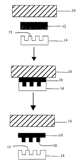
Referring to Fig. l, an optical flat 10, a disk 12, and a master mold 14 are
provided. Disk
12 is formed of a nonstick material such as one of those described above
(e.g., FEP polymer).
Furthermore, disk 12 is preferably ultrasmooth and ultra clean as is commonly
known in the art.
Master mold 14 can be formed of any conventional material and by known
fabrication
methods (e.g., photolithography, e-beam lithography, etc.). Master mold 14 has
a surface 15 that
is patterned with structure and topography as needed for the particular
intended purpose. During
fabrication, the disk 12 is placed between the optical flat 10 and the master
mold 14 as shown
in Fig. 1, with each of the optical flat 10 and the master mold 14 preferably
being in contact with
respective hotplates. Furthermore, the surface 15 of the master mold 14 is
positioned adjacent
(i.e., facing) the dislc 12.
The disk 12 is then pressed against the optical flat as illustrated for
sufficient time,
pressure, and temperature (depending upon the properties of the material of
which disk 12 is
formed) to cause disk 12 to be imprinted by surface 15, with the surface 15
and optical flat 10
being maintained substantially parallel to one another during the course of
the entire press
process. After pressing, the combination is preferably allowed to cool, and
the optical flat 10
and master mold 14 are separated in order to remove the resulting nonstick
mold 16. As shown,
nonstick mold 16 now has a negative pattern 18 of the master mold surface 15.
CA 02462347 2004-03-30
WO 03/031096 PCT/US02/32655
8
Referring to Fig. 2, the nonstick mold 16 can now be used to form patterns on
imprintable
or impressible surfaces. Thus, in addition to the optical flat 10, a moldable
or imprintable
material 20 and a substrate 22 are provided, with the material 20 being in
contact with the
substrate 22. Material 20 is preferably a flowable composition that can be
photocured or
thermocured, or that is thermoplastic. The material 20 can be applied to the
substrate 22 by any
known methods (e.g., spin-coating). The material 20 should be applied to the
substrate 22 at a
thickness that is preferably greater than the topography of the negative
pattern 18.
The optical flat 10 and the substrate 22 are spaced apart with the nonstick
mold 16
positioned therebetween. It is important that the negative pattern 18 of
nonstick mold 16 be
faced towards the impressible material 20. The pattern 18 and substrate 22 are
preferably
maintained substantiallyparallel to one another. Optical flat 10 and substrate
22 are then pressed
together (again, for time, temperature and pressure suitable for the
properties of the particular
impressible material 20 being utilized) so as to cause the negative pattern 18
to be transferred to
the impressible material 20, thus resulting in a precursor circuit structure
24 having the desired
pattern 26.
EXAMPLES
The following examples set forth preferred methods in accordance with the
invention.
It is to be understood, however, that these examples are provided by way of
illustration and
nothing therein should be taken as a limitation upon the overall scope of the
invention.
EXAMPLE 1
Fabrication of 1-~,m Topography FEP Patterned Film
and Pattern Transferring Using A Photo-Curable Material
An FEP Teflon~ film (obtained from Du Pont) was trimmed to an appropriate
size. This
FEP film was then thoroughly cleaned to remove organic residue and particles
at its surface. The
FEP film was placed onto a pre-cleaned object surface with 1-~m topography
line structures.
The line width was from 12.5-~m to 237.5-Vim. This patterned object surface
was used as the
master mold. Another object with an ultra-smooth surface was placed on top of
the FEP film
with the smooth surface facing the FEP film. The master mold/FEP film/smooth
surface obj ect
CA 02462347 2004-03-30
WO 03/031096 PCT/US02/32655
9
stack was heated to 2~0 °C. A total pressure of 64 psi was applied from
the top and bottom sides
of the stack. This pressure was applied for 5 minutes. The press process was
carried out under
ambient atmospheric conditions, although it could also be carried out in a
vacuum and under
other conditions. This pressure was applied for 5 minutes. The pressure was
then released, and
the stack was cooled to room temperature and disassembled. The negative
pattern of the master
mold was transferred to the FEP film surface. The resulting patterned FEP film
was greater than
6 inches in diameter and could be used as a mold to transfer patterns to other
substrate surfaces
as described below.
A photo-curable epoxy composition was formed by mixing a novolac epoxy (50
wt%,
Dow Chemical DEN431) with propylene glycol methyl ether acetate (50 wt%).
Next, 1-3 wt%
of triarylsulphonium hexafluorophosphate (a photo-acid generator) was added to
this mixture,
with the percentage by weight of triarylsulphonium hexafluorophosphate being
based upon the
weight of the novolac epoxy that was utilized.
A 1.5-pm thiclc film of the photo-curable epoxy composition was coated onto a
6-inch
silicon wafer surface. The wafer was placed onto a wafer stage in a press
chamber with the
epoxy-coated surface facing a UV-transparent, optical flat object. The
patterned FEP film was
placed between the wafer and the optical flat obj ect, with the patterned
surface facing the epoxy-
coated wafer. The press chamber was sealed and evacuated to less than 20 Torr,
and the wafer
stage was raised to press the wafer against the patterned FEP film which, in
turn, pressed against
the optical flat surface with a pressure of 64 psi for 1 minute. While the FEP
film was in contact
with the optical flat surface, UV light was illuminated through the optical
flat to cure the epoxy.
Once the epoxy was cured, the press pressure was released. The wafer stage was
lowered, and
the chamber was vented. The patterned FEP film was separated from the wafer
surface. The
pattern of the master mold with 1-p,m topography was transferred to the 6-inch
epoxy-coated
wafer surface.
EXAMPLE 2
Pattern Transferring Using a Radiant Thermal Process
With a 1-pm Topography FEP Patterned Film
A 15-~m pre-polymer (dry etch benzocyclobutene, hereinafter referred to as
"dry etch
BCB," available from Dow Chemicals, CYCLOTENE 3000 series) was coated onto a 6-
inch
CA 02462347 2004-03-30
WO 03/031096 PCT/US02/32655
silicon wafer surface. This wafer was balced at 135 °C for 7 minutes.
The wafer was then
transferred to the preheat wafer stage, which was set at a temperature of
150°C, in a press
chamber with the polymer-coated surface facing an optical flat object. The
patterned FEP film
used in Example 1 was placed between the wafer and the optical object, with
the patterned
5 surface facing the polymer-coated wafer surface. The press chamber was
sealed and evacuated
to less than 20 Torr, and the wafer stage was raised to press the wafer
against the patterned FEP
film which, in turn, pressed against the optical flat surface with a press
pressure of 64 psi for 1
minute. The wafer stage was then cooled to less than 50°C, with the
press pressure being
maintained during cooling. The wafer stage was lowered, and the chamber was
vented. The
10 patterned FEP film was then separated from the wafer surface. The pattern
of the master mold
with 1-p,m topography had been successfully transferred to the polymer-coated
wafer surface.
EXAMPLE 3
Pattern Transfernng Using an Infrared (IR) Thermal Process
With a 1-~,m Topography FEP Patterned Film
A 15-p,m thick film of dry etch BCB was coated onto a 6-inch silicon wafer
surface. This
wafer was baked at 135 °C for 7 minutes. The wafer was then transferred
to the wafer stage in
a press chamber with the polymer-coated surface facing an IR-transparent
optical flat obj ect. The
patterned FEP film used in Example 1 was placed between the wafer and the
optical obj ect, with
the patterned surface facing the polymer-coated wafer surface. The press
chamber was sealed
and evacuated to less than 20 Torr. IR light was illuminated through the
optical object and FEP
film to heat the polymer until it reached its flow temperature. The wafer
stage was then raised
to press the wafer against the patterned FEP film which, in turn, pressed
against the optical flat
surface with a pressure of 64 psi for 1 minute as the IR heating was continued
to maintain the
flow temperature. The IR heating was stopped, and the wafer was then cooled
for 30 seconds.
The press pressure was released. The wafer stage was lowered, and the chamber
was vented.
The patterned FEP film was separated from the wafer surface. The pattern of
the master mold
with 1-pm topography had been transferred to the polymer-coated wafer surface.
CA 02462347 2004-03-30
WO 03/031096 PCT/US02/32655
11
EXAMPLE 4
Fabrication of a 0.5-p,m Topography FEP Patterned Finn
and Pattern Transferring Using a Photo-Curable Material
An FEP Teflon~ film was trimmed to the desired size. This FEP film was then
thoroughly cleaned to remove organic residue and particles from its surface.
The film was placed
onto a pre-cleaned obj ect surface having 0.5-p,m topography with feature
sizes ranging from 3-
~m to 500-~.m structures. This patterned object surface was used as the master
mold. Another
object with an ultra-smooth surface was placed on top of the FEP film with the
smooth surface
facing the FEP film. The master mold/FEP film/smooth object stack was heated
to 280°C. A
total pressure of 64 psi was applied from the top and bottom sides of the
stack for 5 minutes. The
press process was carned out under an ambient atmosphere. After the pressure
was released, the
stack was cooled to room temperature. The stack was then disassembled. The
negative pattern
of the master mold was transferred to the FEP film surface. This patterned
surface on the FEP
film was greater than 6 inches in diameter and was then used as a mold to
transfer patterns to
other substrate surfaces as described below.
A 1.5-~m thick layer photo-curable epoxywas coated onto a 6-inch silicon wafer
sur face.
This wafer was placed onto a wafer stage in a press chamber with the epoxy-
coated surface
facing a UV-transparent optical flat object. The patterned FEP film was placed
between the
wafer and optical flat obj ect, with the patterned surface facing the epoxy-
coated wafer. The press
chamber was sealed and evacuated to less than 20 Torr. The wafer stage was
raised to press the
wafer against the patterned FEP film which pressed against the optical flat
surface with a
pressure of 64 psi for 1 minute. While still in contact with the optical flat
surface, UV light was
illuminated through the optical flat surface to cure the epoxy. Once the epoxy
had cured, the
press pressure was released, the wafer stage was lowered, and the chamber was
vented. The
patterned FEP film was separated from the wafer surface, and the pattern of
the master mold with
0.5-pm topography had been transferred to the 6-inch epoxy-coated wafer
surface.
CA 02462347 2004-03-30
WO 03/031096 PCT/US02/32655
12
EXAMPLE 5
Pattern Transferring Using a Radiant Thermal Process
With a 0.5-p.m Topography FEP Patterned Film
A 15-~m thick layer of dry etch BCB was coated onto a 6-inch silicon wafer
surface.
This wafer was baked at 135 ° C for 7 minutes. The wafer was then
transferred to the wafer stage,
which had been preheated to a temperature of 150 ° C, in a press
chamber with the polymer-coated
surface facing an optical flat object. The patterned FEP film used in Example
4 was placed
between the wafer and optical object. The press chamber was sealed and
evacuated to less than
20 Torr, and the wafer stage was raised to press the wafer against the
patterned FEP film which
then pressed against the optical flat surface with a pressure of 64 psi for 1
minute. The wafer
stage was then cooled to less than 50°C, while the press pressure was
maintained. After the
wafer stage had cooled, it was lowered, and the chamber was vented. The
patterned FEP film
was then separated from the wafer surface. The pattern of the master mold with
0.5-~.m
topography was successfully transferred to the polymer-coated wafer surface.
EXAMPLE 6
Pattern Transferring Using an Infrared (IR) Thermal
Process With a 0.5 wm Topography FEP Patterned Film
A 15-~.m thick layer of dry etch BCB was coated onto a 6-inch silicon wafer.
This wafer
was baked at 135 °C for 7 minutes. The wafer was then transferred to
the wafer stage in a press
chamber with the polymer-coated surface facing an IR-transparent optical flat
object. The
patterned FEP film used in Example 4 was placed between the wafer and the
optical obj ect. The
press chamber was sealed and evacuated to less than 20 Torr. IR light was
ilhuninated through
the optical object to heat the polymer to its flow temperature. The wafer
stage was then raised
to press the wafer against the patterned FEP film which then pressed against
the optical flat
surface with a pressure of 64 psi for 1 minute. IR heating was continued to
maintain the flow
temperature during the press process. IR heating was then stopped, the wafer
was cooled for 30
seconds, and the press pressure was released. The wafer stage was lowered, and
the chamber was
vented. The patterned FEP film was then separated from the wafer surface. The
pattern of the
master mold with 0.5-p,m topography had been transferred to the polymer-coated
wafer surface.
CA 02462347 2004-03-30
WO 03/031096 PCT/US02/32655
13
EXAMPLE 7
Fabrication of 5-p,m Topography FEP Patterned
Filin and Pattern Transferring Using a Thermo-Curable Material
An FEP Teflon' filin was trimmed to an appropriate size. This FEP film was
thoroughly
cleaned to remove organic residue and particles at its surface. This FEP fihn
was placed onto
a pre-cleaned object surface with 5-~m topography with feature sizes in the
range of 50-pm to
over 5000-~m structures. This patterned object surface was used as the master
mold. Another
object with an ultra-smooth surface was placed on top of the FEP film with the
smooth surface
facing the FEP film. The master mold/FEP film/smooth object surface stack was
heated to
280°C. A total pressure of 35 psi was applied from the top and bottom
sides of the stack. The
pressure was applied for 4 minutes. The press process for this sample was
carried out under
ambient atmospheric conditions. The pressure was released, and the stack was
cooled to room
temperature. The stack was then disassembled, and the pattern of the master
mold was
transferred to the FEP film surface. The result was a patterned FEP film
greater than 6 inches
in diameter that was used as a mold to transfer patterns to other substrate
surfaces.
A >5-~,m thick film of dry etch BCB was coated onto a 6-inch silicon wafer
surface. This
wafer was baked at 150°C for 1 minute. The wafer was then transferred
to the preheat wafer
stage (temperature of 175°C) in a press chamber with the polymer-coated
surface facing an
optical flat obj ect. The patterned FEP film, with 5-p.m topography, was
placed between the wafer
and the optical flat object. The wafer stage was raised to press the wafer
against the patterned
FEP film which, in turn, pressed against the optical flat surface with a press
pressure of 21 psi
for 5 minutes. The entire pressed obj ect was then cooled to <75 ° C,
with the press pressure being
maintained at 21 psi. The press pressure was then released, and the wafer
stage was lowered.
The stack was removed from the press tool and allowed to cool to room
temperature. The stack
was disassembled, and the patterned FEP film was subsequently separated from
the wafer
surface. The pattern of the master mold with 5-~m topography was transferred
to the polymer-
coated wafer surface.
CA 02462347 2004-03-30
WO 03/031096 PCT/US02/32655
14
EXAMPLE 8
Fabrication of 1-~,m Topography FEP Patterned Film with
0.25-~,m Structures and Pattern Transferring Using A Photo-Curable Material
An FEP Teflon~ film was trimmed to an appropriate size. This FEP film was
thoroughly
cleaned to remove organic residue and particles at its surface. The FEP film
was then placed
onto a pre-cleaned obj ect surface with 1-~m topography with feature sizes of
from 0.25-~.m to
50-~.m structures. This patterned object surface was used as the master mold.
Another object
with an ultra-smooth surface was placed on top of the FEP film with the smooth
surface facing
the FEP film. The master mold/FEP film/smooth surface object staclc was heated
to 280°C. A
total pressure of 64 psi was applied from the top and bottom sides of the
stack. This pressure was
applied for 5 minutes. The press process was carried out under ambient
atmospheric conditions.
The pressure was then released, and the stack was cooled to room temperature
and then
disassembled. The negative pattern of the master mold had been transferred to
the FEP film
surface. The result was a patterned FEP film (with a diameter of greater than
6 inches) which
was used as a mold to transfer patterns to other substrate surfaces.
A 1.5-~m thick photo-curable epoxy was coated onto a 6-inch silicon wafer
surface. This
wafer was placed onto a wafer stage in a press chamber with the epoxy-coated
surface facing a
UV-transparent optical flat object. The patterned FEP film was placed between
the wafer and
the optical flat object, with the patterned surface facing the epoxy-coated
wafer. The press
chamber was sealed and evacuated to less than 20 Torr, and the wafer stage was
raised to press
the wafer against the patterned FEP film which, in turn, pressed against the
optical flat surface
with a pressure of 64 psi for 1 minute. While the FEP film was in contact with
the optical flat
surface, UV light was illuminated through the optical flat surface to cure the
epoxy. After the
epoxy was cured, the press pressure was released. The wafer stage was lowered,
the chamber
was vented, and the patterned FEP film was separated from the wafer surface.
The pattern of the
master mold of 1-~,m topography with 0.25-~m structures was transferred to the
6-inch, epoxy-
coated wafer surface.
CA 02462347 2004-03-30
WO 03/031096 PCT/US02/32655
EXAMPLE 9
Pattern Transferring at Elevated Temperature
Using a Photo-Curable Material
A layer approximately 13-~m thick of a UV curable material (photosensitive
5 benzocyclobutene, sold by Dow Chemicals under the name CYCLOTENE 4000
series) was
coated onto a 6-inch silicon wafer. The wafer was then transferred onto a
wafer stage (preheated
to 135 °C) in a press chamber with the polymer-coated surface facing a
UV transparent optical
flat obj ect. The patterned FEP film used in Example 4 was placed between the
wafer and optical
obj ect, with the patterned surface facing the wafer. This wafer was baked on
the wafer stage for
10 1 minute. The press chamber was sealed and evacuated to less than 20 Torr.
While at 135 °C,
the wafer stage was raised to press the wafer against the patterned FEP film
which pressed
against the optical flat surface with a press pressure of 64 psi for 1 minute.
While still in contact
with the optical flat surface, UV light was illuminated through the optical
flat to cure the coated
material. Once the material was cured, the press pressure was released, the
wafer stage was
15 lowered, and the chamber was vented. The patterned FEP film was separated
from the wafer
surface. The pattern of the master mold with 0.5-pm topography was transferred
to the 6-inch
wafer surface.
EXAMPLE 10
Fabrication of 1-~m Topography FEP Patterned Film from
FEP Pellets and Pattern Transferring Using a Photo-Curable Material
A pre-cleaned object surface with 1-pm topography line structures was placed
onto a
substrate stage. The line sh~uctures on the object surface were 12.5 ~m to
237.5 ~m wide. This
patterned object surface was used as the master mold. The patterned object
surface was covered
with an FEP resin that was in the form of about 2-3 mm pellets. Another object
with an ultra-
smooth surface was place on top of the FEP pellets with the smooth surface
facing the FEP
material. This master mold/FEP pellets/optical flat obj ect stack was heated
to 280 ° C. A total
pressure of 64 psi was applied from the top and bottom sides of the stack for
5 minutes. The
press process was carned out under ambient atmospheric conditions. The
pressure was then
CA 02462347 2004-03-30
WO 03/031096 PCT/US02/32655
16
released, and the stack was cooled to room temperature and disassembled. An
FEP film with a
negative pattern of the master mold was fabricated from the FEP pellets. This
patterned FEP film
(which was greater than 6 inches in diameter) was then used as a mold to
transfer patterns to
other substrate surfaces.
A 1.5-~m thick film of photo-curable epoxy was coated onto a 6-inch silicon
wafer
surface. The wafer was placed onto a wafer stage in a press chamber with the
epoxy-coated
surface facing a UV-transparent optical flat object. The patterned FEP film
was placed between
the wafer and the optical flat object, with the patterned surface facing the
epoxy-coated wafer.
The press chamber was sealed and evacuated to less than 20 Torr, and the wafer
stage was raised
to press the wafer against the patterned FEP film which pressed against the
optical flat surface
with a pressure of 64 psi for 30 seconds. While the FEP film was in contact
with the optical flat
surface, UV light was illuminated through the optical flat to cure the epoxy.
Once the epoxy was
cured, the pressure was released, the wafer stage was lowered, and the chamber
was vented. The
patterned FEP film was separated from the wafer surface. The pattern of the
master mold with
1-p.m topography was transferred to the 6-inch epoxy-coated wafer surface.
EXAMPLE 11
Pattern Transferring Using a Thermal Process with
Infrared (IR) Wafer Backside Heating
A 15-~,m thick film of dry etch BCB was coated onto a 6-inch silicon wafer.
This wafer
was baked at 135 ° C for 7 minutes. A patterned FEP film with a 0.5-~m
topography pattern was
placed onto the wafer stage in the press chamber, with the patterned surface
of the film facing
away from the stage surface. The polymer-coated wafer was transferred into the
press chamber.
The wafer was placed between the FEP film and an optical flat object with the
polymer-coated
surface facing the patterned FEP film surface. The backside of the wafer was
facing the optical
flat object. The press chamber was sealed and evacuated to less than 20 Torr.
An infrared (IR)
light was illuminated through the optical object to heat up the backside of
the wafer to reach the
polymer flow temperature. The wafer stage was then raised with a press
pressure of 64 psi for
2 minutes in order to cause the FEP film to press against the polymer-coated
wafer which pressed
against the optical flat object surface. During the press process, the press
temperature was
maintained by IR illumination through the optical flat obj ect. The wafer was
then cooled for 1
CA 02462347 2004-03-30
WO 03/031096 PCT/US02/32655
17
minute, without IR heating, to below the flow temperature of the coated
polymer. The press
pressure was released, and the wafer stage was lowered. The press chamber was
vented, and the
patterned FEP film was separated from the wafer surface. The pattern of the
master mold with
0.5-~,m topography was transferred to the polymer-coated wafer surface.
EXAMPLE 12
Pattern Transferring Using a Thermoplastic Material
A 2.7-~m thermoplastic material, polymethyl methacrylate (PMMA), was coated
onto
a 6-inch silicon wafer surface. This wafer was baked in the press chamber at
120°C for 30
seconds on the preheat wafer stage, with the polymer-coated surface of the
wafer facing an
optical flat obj ect. The patterned FEP film with 1-pm topography was placed
between the wafer
and the optical flat object. The wafer stage was raised to press the wafer
against the patterned
FEP film which, in turn, pressed against the optical flat surface with a press
pressure of 34 psi
for 5 minutes. The press pressure was released, and the wafer stage was
lowered. The
wafer/FEP film/optical flat object stack was removed from the press tool and
allowed to cool to
room temperature, and the stack was disassembled. Subsequently, the patterned
FEP film was
separated from the wafer surface. The pattern of the master mold with 1.0-~m
topography was
transferred to the PMMA-coated wafer surface.
EXAMPLE 13
Rolling Pattern Transferring
A patterned FEP film was attached onto a 4.5-inch diameter cylinder with the
patterned
surface facing outward. A 15-~m thick pre-polymer dry etch BCB was coated onto
a 6-inch
silicon wafer surface. This wafer was baked at 150°C for 1 minute. The
FEP film-attached
cylindrical object was rolled evenly across the wafer surface at 150°C
in about 3 seconds. The
heat source was removed from the wafer and allowed to cool to room
temperature. The pattern
of the master mold with 1-~.m topography was transferred to the polymer-coated
wafer surface.
This example was successfully repeated with a baking temperature of 100
° C for 1 minute and
a rolling temperature of 100°C for 5 seconds.