Note: Descriptions are shown in the official language in which they were submitted.
CA 02462504 2004-03-31
WO 03/030389 PCT/US02/11504
[0001 ] CODE TRACKING LOOP WITH
AUTOMATIC POWER NORMALIZATION
[0002] BACKGROUND
[0003] The present invention relates to a code tracking system for a receiver
of a
code division multiple access (CDMA) communication system. More specifically,
the
present invention relates to a second order code tracking system for more
effectively
removing the timing difference between the transmitted code and the received
code.
[0004] Synchronization is an important task in any kind of telecommunication.
There are several levels of synchronization, such as, carrier, frequency,
code, symbol,
frame and network synchronization. In all these levels, synchronization can be
distinguished into two phases, which are acquisition (initial synchronization)
and
tracking (fine synchronization).
[0005] A typical wireless communication system sends downlink communications
from a base station to one or a plurality of User Equipments (UEs) and uplink
communications from UEs to the base station. A receiver within the UE works by
correlating, or despreading, the received downlink signal with a known code
sequence.
The sequence must be exactly synchronized to the received sequence in order to
get
the maximal output from the correlator. The receiver should be able to easily
adapt to
a change in the environment of a radio line changing without ceasing
operation. In
order to accomplish this, present receivers gather as much of the transmitted
signal
energy as possible in order to maximize the signal-to-noise ratio. In mufti-
path fading
channels, however, the signal energy is dispersed over a certain amount of
time due to
distinct echo paths and scattering. One crucial task of the receiver is thus
to estimate
the channel to improve its performance. If the receiver has information about
the
channel profile, one way of gathering signal energy is then to assign several
correlator
branches to different echo paths and combine their outputs constructively, a
structure
known as the RAKE receiver.
-1-
CA 02462504 2004-03-31
WO 03/030389 PCT/US02/11504
[0006] The RAKE receiver has several fingers, one for each echo path, and in
each
finger, the path delay with respect to some reference delay such as a direct
or the
earliest received path, must be estimated and tracked throughout the
transmission. The
estimation of the paths initial position in time is obtained by using a mufti-
path search
algorithm. The mufti-path search algorithm does an extensive search through
correlators to locate the paths with a chip accuracy. After these initial
positions are
found, the tracking units generate accurate estimates for the delays of
several multi-
path components by means of early-late timing error detectors and utilize
these
estimates for the different delays to shift the phase of the codes. This type
of tracking
unit is known as an early-late gate synchronizer. A delay-locked loop (DLL) is
commonly used to implement the early-late gate synchronizer. Illustrated in
Figure 1
is a block diagram of this delay-locked loop. The bandwidth of the Code
Tracking
Loop (CTL) determines the noise filtering capability of the synchronizer. The
narrower
the bandwidth, the more robust the synchronizer is to distortion from noise
and less
sensitive to small signal changes. The bandwidth of the loop depends on the
parameters of the loop filter (alpha, beta), total loop gain ( KT ), and input
signal power
level ( P,n ). Damping ratio of the loop also depends on the same parameters.
Damping
ratio of the loop determines the stability of the loop. Although the
parameters of the
loop can be fixed, it is very difficult to fix the input signal level.
[0007] Most of the digital receivers employ some form of Automatic Gain
Control
(AGC) in their physical layers. Although AGC limits the input signal level,
the
dynamic level of the signal level is still large. This is due to the fact that
AGC is
actually designed to prevent the Analog to Digital Converter (ADC) from
entering
saturation.
[0008] Since the dynamic range of the input signal level is not effectively
limited,
the bandwidth and damping ratio of the code tracking loop changes with input
signal
power. This results in degradation in performance for the code tracking loop.
-2-
CA 02462504 2004-03-31
WO 03/030389 PCT/US02/11504
[0009] Accordingly, there exists a need for a code tracking loop that
maintains the
bandwidth and damping ratio of the loop regardless of changes with the input
signal
power level.
[00010] Other objects and advantages of the present invention will become
apparent after reading the description of the preferred embodiment.
[00011 ] SUMMARY
[00012] The present invention is a receiver, included in a user equipment
(UE), of a
code division multiple access (CDMA) communication system which includes the
UE
and a plurality of base stations. The UE is in communication with one of the
plurality
of base stations and receives a communication signal from the base station
through the
receiver. The communication signal is correlated by said receiver using a
delay locked
code tracking loop, that estimates and tracks a channel delay of the
communication
signal. The tracking loop comprises a reference code generator for generating
a
reference code signal and an interpolator for generating timed signal versions
in
response to the receipt of said communication. A timed signal correlator, also
included
in the track loop for correlating at least two of the timed signal versions
with the code
reference signal. The result of the correlation is used for generating an
error signal.
An automatic power normalization loop (APN), which is responsive to the
interpolator,
generates a power error signal that is used to normalize the error signal
through a
normalization circuit.
[00013] BRIEF DESCRIPTION OF THE DRAWINGS)
[00014] Figure 1 is a block diagram of a prior art delay-locked tracking loop.
[00015] Figure 2 is a block diagram of a delay-locked code tracking loop with
automatic power normalization in accordance with the present invention.
[00016] Figure 3 is a flow diagram of the delay-locked code tracking loop of
the
present invention.
-3-
CA 02462504 2004-03-31
WO 03/030389 PCT/US02/11504
[00017] Figure 4 is a block diagram of an exemplary loop filter included in
the
delay-locked tracking loop of the present invention.
[00018] DETAILED DESCRIPTION OF THE PREFERRED EMBODIMENTS)
[00019] The preferred embodiment will be described with reference to the
drawing
figures wherein like numerals repeat like elements throughout.
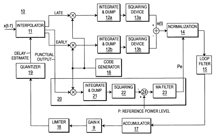
[00020] Illustrated in Figure 2 is a block diagram of the delay-locked code
tracking
loop (DCTL) 10 in accordance with the preferred embodiment of the present
invention.
The DCTL comprises an interpolator 1 l, two integrate and dump devices 12a,
12b,
two squaring devices 13a, 13b, a normalization device 14, a loop filter 15, a
code
generator 16, an accumulator 17, a limiter 18, a quantizer 19, a gain circuit
9, and an
automatic power normalization loop (APN) 20. The delay-lock code tracking loop
10
receives an input signal x (t-T), where T is the timing error in the received
signal.
Since the timing error is confined to -Tc to Tc , where Tc is the chip
duration using
the multi-path search algorithm, the only way to shift the incoming signal is
by using
mathematical interpolation. Accordingly, the interpolator 11, coupled to the
integrate
devices 12a, 12b, the code generator 16, and the APN 20, receives the input
signal x (t-
T) and creates three outputs: Punctual, Early and Late. As those skilled in
the art
know, the Early and Late outputs are a half chip early and a half chip late
versions of
the punctual output, respectively. They are all obtained by interpolation of
the
incoming signal x (t-T). After the interpolator 11, down-sampling takes place,
all three
outputs are preferably down-sampled by an over-sampling ratio of the
transmitted
signal. The punctual output is the main output of the DCTL 10, the early and
late
outputs are used only inside the code tracking loop 10 algorithm.
[00021 ] The early and late signals are correlated with the output of the
reference
code generator 16, such as a pilot code generator, in lower and upper branches
of the
DCTL using the integrate devices 12a, 12b, respectively. Once the outputs of
the code
generator 16 and the early and late outputs have been correlated, the
correlated signals
-4-
CA 02462504 2004-03-31
WO 03/030389 PCT/US02/11504
are forwarded to squaring devices 13a, 13b, respectively. Since phase
synchronization
is not acquired at this stage, squaring is used to obtain non-coherent CTL.
[00022] After correlation and squaring, the difference of the two branches
(early and
late) are taken to produce an error signal e(t), which is proportional to the
timing error.
The error signal e(t) is then power normalized against a power error signal
(Pe) by the
normalization circuit 14 (to be disclosed hereinafter) and output to the loop
filter 15.
[00023] The loop filter 15, coupled to the normalization device 14 and the
accumulator 17, filters the normalized error signal e(t) and forwards it to
the
accumulator 17. An exemplary loop filter is a classical proportional
integrator (PI)
filter, but any first order low-pass filter would be appropriate for the
present invention.
The PI filter, including a loop filter accumulator 41, has two branches, as
shown in
Figure 4. One branch creates a control signal proportional to the current
value of the
error signal and the other branch produces a signal proportional to the
average value of
the error signal. These signals are combined after being multiplied by two
different
constants, alpha and beta. The accumulator 41 inside the PI filter works
exactly the
same way as the accumulator 17 described below.
[00024] The accumulator 17, coupled to the loop filter and a gain circuit 9,
receives
the filtered error signal from the loop filter 15 and processes the signal.
Those having
skills in the art know that the accumulator 17 simply adds its current input
to its
previous output. Initially, the output of the accumulator 17 is set to zero.
There is an
overflow detection inside the accumulator to limit the output value. The
accumulation
by the accumulator 17 together with the loop filter 15 is used to obtain the
second
order feedback loop response. The accumulator 17 then forwards the error
signal e(t)
to the gain circuit 9.
[00025] The gain circuit 9, coupled to the accumulator 17 and a limiter
circuit 18,
receives the output of the accumulator 17 and adjust the level of the filtered
signal to
match the interpolator 11 timing shift value. This circuit changes the sign in
the timing
air signal to correct the timing delay/advance of the incoming signal
reference to the
code generator 16. Once this is accomplished, the gain circuit 9 forwards the
adjusted
-5-
CA 02462504 2004-03-31
WO 03/030389 PCT/US02/11504
error signal e(t) to a limner circuit 18 that limits the over shoot of the
error signal if it
is above the chip duration -Tc to Tc. The limiter 18 forwards the error signal
to the
quantizer 19 where the discrete value of the delay estimate is obtained and
forwarded
back to the interpolator 11. In this design, a thirty-two (32) level quantizer
is used to
obtain an accuracy of Tcll6. Although any level of quantizer can be used for
different
levels of delay estimate accuracy.
[00026] DCTL is a second order feedback loop. In control system notation, the
system function, H(s), for a second order feedback loop can be written as
H(s) = 2~~'ns + ~" , Equation ( 1 )
s2 +2~t~"s+~n
where ~' is the damping ratio and ~n is the natural frequency of the system.
These can
be written in terms of the parameters of the DCTL as follows:
r~" = 2 P,n KT~ , Equation (2)
KTa P"
_ , Equation (3)
~n
where alpha and beta are the loop filter parameters, KT = KSK is the total
open loop
gain including the S-curve gain and the external gain, and P," is the input
signal power.
The two-sided noise bandwidth of the system is given by
W, = ran (~' + 4~ ) . Equation (4)
As an example, a Universal Mobile Telecommunications System (LTMTS) Frequency
Division Duplex (FDD) IJE receiver design with a chip rate of 3.84 MHz and 2
times
over-sampling use the following values: spreading factor of 256 for the pilot
code,
loop gain K = 0.01, alpha = 0.0141, and beta = 0.00001. The values of natural
frequency and damping ratio determine the main characteristics of the loop
such as
stability, gain and phase margins, bandwidth, convergence time, and steady
state fitter.
These characteristics are fixed during the design and should not change with
respect to
the input. Otherwise, the DCTL may malfunction and produce unexpected results.
-6-
CA 02462504 2004-03-31
WO 03/030389 PCT/US02/11504
However, as seen from equations 2, 3, and 4, they all depend on input signal
power,
P,n , which may change considerably during the communication process.
[00027] In order to overcome the effects of the input signal x (t-T) power
level
changing, an Automatic Power Normalization loop 20 (APN) is included in the
delay-
locked tracking loop 10 of the present invention. The APN 20, coupled to the
interpolator 11, the code generator 16 and the normalization circuit 11,
comprises an
integrate and dump circuit 21, a squaring device 22, an adder 24, and a moving
average
(MA) filter 23. The punctual output from the interpolator 11 is the input to
the APN
loop 20. The punctual signal is received by the integrate and dump circuit 21
along
with the signal from the code generator 16. The integrate and dump circuit 21
is
coupled to the code generator 16, the interpolator 11, and the squaring device
22.
Similar to the integrate and dump circuits 12a, 12b disclosed above, the
integrate and
dump circuit 21 correlates the punctual signal received from the interpolator
11 with
the signal received from the reference code generator 16. Once the two signals
are
correlated the integrate circuit 21 forwards the correlated signal to the
squaring device
22.
[00028] The squaring device 22, coupled to the integrate circuit 21 and the
adder 24,
squares the correlated signal and forwards the squared signal to the adder 24.
The
adder 24 subtracts the squared output from the squaring device 22 from a
reference
signal power (P) the reference signal power (P) is a predetermined value and
is used in
the design of the DLL 10 to set the parameters. As those skilled in the art
know, the
reference power level (P) may be any predetermined value. The subtracting of
the
squared signal by the adder 24 results in a power difference signah which is
forwarded
to the moving average filter 23.
[00029] The Moving Average (MA) filter 23, coupled to the adder 24 and the
normalization circuit 14, receives the difference signal and filters it. The
MA filter 23
consists of a real valued register of size N, an adder, and a constant
multiplier with a
factor of 1/N. Each time a new input is passed to the MA filter 23 the
register elements
are shifted one to the right. The element that came the earliest (on the right
most side)
_7_
CA 02462504 2004-03-31
WO 03/030389 PCT/US02/11504
is cleared and the current input value is placed in the left most place in the
register.
After this shift, each element in the register is added. The total value is
multiplied by
1/N to produce the average value for the power error signal (Pe). It is
preferable that
N be selected to be twenty (20), which corresponds to 20 symbols processed.
The MA
filter size is selected such that it will be insensitive to instantaneous
power changes due
to fading, however it will compensate for the average input signal level
changes. Once
the MA filter 23 filters the power difference signal, a filtered power error
signal Pe is
forwarded to the normalization circuit 14.
[00030] The normalization circuit 14, coupled to the squaring devices 13a, 13b
and
the APN 20, receives the error e(t) corresponding to the difference between
the late and
early outputs of the interpolator 11 and the power error signal Pe from the
APN 20. In
order to normalize the error signal e(t) against the power error signal Pe,
the
normalization circuit 14 multiplies the error signal e(t) by (P/(P+ pe)),
where P is the
referenced signal power level used in the APN loop 20.
[00031 ] The normalization of the error signal instead of the input signal
results in a
reduced number of multiplications (normalization) by a factor equal to the
spreading
factor. Preferably, integrated into the normalization circuit there is a
limner (not
shown) that limits the multiplication factor from 0.1 to 10 or -20dB to 20 dB.
This
limiter is used to prevent noise amplification.
[00032] The flow diagram of the delay-lock code tracking loop in accordance
with
the preferred embodiment of the present invention is illustrated in Figure 3.
An input
signal in received by the DLL circuit 10 (step 301). The interpolator 11 of
the DLL
circuit 10 produces the late, early and punctual outputs (step 302). The late
and early
outputs are correlated with the code generator 16 (step 303a), and the
difference
between the correlated signals is determined, producing an error signal e(t)
(step 304a).
Simultaneous to the late and early outputs, the punctual output is correlated
with the
code generator (step 303b) and subtracted from a predetermined reference power
level
to produce a power level difference signal (step 304b). The power level
difference
signal is then filtered to produce a power level error signal Pe (step 305b).
The error
_g_
CA 02462504 2004-03-31
WO 03/030389 PCT/US02/11504
signal corresponding to the late and early outputs, is normalized against the
power
level error signal Pe from the APN loop 20 (step 306). The normalized error
signal is
then processed to produce a delay estimate (step 307) which is forwarded back
to the
input of the DLL tracking loop 10 (step 308).
[00033] While the present invention has been described in terms of the
preferred
embodiment, other variations which are within the scope of the invention as
outlined in
the claims below will be apparent to those skilled in the art.
-9-