Note: Descriptions are shown in the official language in which they were submitted.
CA 02462844 2004-04-02
FP02-0155-00
DESCRIPTION
TEMPERATURE-COMPENSATED OPTICAL COMMUNICATION
INTERFERENCE DEVICE AND OPTICAL COMMUNICATION SYSTEM
Technical Field
The present invention relates to an optical
device configured to divide input light into two beams,
thereafter let the two beams interfere with each other,
and then output the recombined light.
Background Art
The optical devices configured to divide input
light into two beams, thereafter let the two beams
interfere with each other, and then output the
recombined light, include the known Mach-Zehnder
interferometer type device and Michelson interferometer
type device.
A Mach-Zehnder interferometer type optical device
comprises an optical divider and an optical coupler.
There are first and second optical paths provided
between the optical divider and the optical coupler.
When light enters an input port of this optical device,
the light is divided into two beams by the optical
divider. One divided beam travels on the first optical
path. The other divided beam travels on the second
optical path. These divided beams travel through the
first optical path and through the second optical path,
respectively, up to the optical coupler. The optical
1
CA 02462844 2004-04-02
FP02-0155-00
coupler couples these divided beams with each other.
The coupled light goes out through an output port of
the optical device. The transmission characteristic
(the relation between wavelength and transmittance) of
this optical device is dependent on the light dividing
property of the optical divider and the light coupling
property of the optical coupler, and further on the
difference between the lengths of the first and second
optical paths.
A Michelson interferometer type optical device
comprises a beam splitter serving as both an optical
divider and an optical coupler, and a first mirror and
a second mirror. This optical device has first and
second optical paths. On the first path, a beam going
out from the beam splitter travels to the first mirror
and the beam is reflected by the first mirror back to
the beam splitter. On the second path, a beam going
out from the beam splitter travels to the second mirror
and the beam is reflected by the second mirror back to
the beam splutter. When light enters an input port of
the device, the light is divided into two beams by the
beam splitter. One divided beam travels on the first
optical path, that is, the forward and backward optical
path between the beam splitter and the first mirror.
The other divided beam travels on the second optical
path, that is, the forward and backward optical path
2
CA 02462844 2004-04-02
FP02-0155-00
between the beam splitter and the second mirror. These
divided beams travel through the first and second
optical paths back to the beam splitter. The beam
splitter couples these divided beams with each other
and feeds the coupled light to an output port of the
optical device. The transmission characteristic of
this optical device from the input port to the output
port is dependent on the light dividing property of the
beam splitter and the difference between the lengths of
the first and second optical paths.
Such interference devices can be used as optical
filters with a certain loss spectrum in optical
communication systems. Besides, the interference
devices can also be used as interleavers to demultiplex
signal light of multiple wavelengths into multi
wavelength signal light of even channels and multi
wavelength signal light of odd channels, or as
interleavers to multiplex multi-wavelength signal light
of even channels and multi-wavelength signal light of
odd channels.
As described above, the transmission
characteristic of the Mach-Zehnder interferometer type
or Michelson interferometer type optical device is
dependent on the path length difference between the
first and second optical paths. Accordingly, in order
to keep the transmission characteristic of the optical
3
CA 02462844 2004-04-02
FP02-0155-00
device constant, it is necessary to maintain the path
length difference constant between the first and second
optical paths. For this reason, the optical elements
constituting the optical device are fixed on a
substrate.
In the configuration wherein the optical elements
are fixed on the substrate, however, the path lengths
of the first and second optical paths vary
independently according to expansion or constriction of
the substrate with temperature change, so that the
optical path length difference may change. With change
in the path length difference, the optical device will
also change its transmission characteristic. Thus the
transmission characteristic of the optical device has
temperature dependence.
In order to suppress the temperature dependence,
it is also conceivable to maintain the temperature of
the entire optical device constant. In this case, a
temperature adjusting means is necessary in order to
maintain the temperature constant. It is also
necessary to provide a means for supplying power to the
temperature adjusting means. Therefore, the optical
device has to be constructed in larger scale.
Disclosure of the Invention
An object of the present invention is to provide
a temperature-compensated optical communication
4
CA 02462844 2004-04-02
FP02-0155-00
interference device with reduced temperature dependence
of the transmission characteristic thereof.
A temperature-compensated optical communication
interference device according to the present invention
comprises: first and second ports; an optical divider
for dividing light entering the first port into first
and second light beams; an optical coupler for
receiving the first and second beams to superpose the
beams and feed the superposed light to the second port;
first and second optical paths disposed between the
optical divider and the optical coupler; a first
optical component placed on the first optical path; a
second optical component placed on the second optical
path; and a substrate on which the optical divider, the
optical coupler, the first optical component, and the
second optical component are placed. The optical
coupler and optical divider may be beam splatters. The
fist and second optical components may be mirrors. The
substrate has one or more members with positive
coefficients of linear expansion and one or more
members with negative coefficients of linear expansion.
Temperature dependence of an optical path length
difference between the first and second optical paths
is reduced due to the difference between the signs of
the coefficients of linear expansion.
The beam having passed through the first optical
5
CA 02462844 2004-04-02
FP02-0155-00
path and the beam having passed through the second
optical path interfere with each other in the path from
the optical coupler to the second port. Therefore, the
transmission characteristic of the light traveling from
the first port to the second port is dependent on the
path length difference between the first optical path
and the second optical path. The substrate includes
the members with the coefficients of linear expansion
having different signs. Consequently, it is possible
to cancel out change in the length of the first optical
path and change in the length of the second optical
path with temperature change to suppress change in the
path length difference. Accordingly, the interference
device of the present invention has the transmission
characteristic resistant to changing even when change
in temperature occurs. Since a temperature adjusting
means is not necessary for maintaining the temperature
constant, the interference device of the present
invention can be constructed in small size.
The first optical path may extend above both of
the members with the positive and negative coefficients
of linear expansion. The second optical path may also
extend above both of the members with the positive and
negative coefficients of linear expansion. At least
one of the optical divider, optical coupler, first
optical component and second optical component may be
6
CA 02462844 2004-04-02
FP02-0155-00
placed on the one or more members with positive
coefficients of linear expansion, and the remainder may
be placed on the one or more members with negative
coefficients of linear expansion.
The interference device may constitute a Mach-
Zehnder interferometer or may constitute a Michelson
interferometer. The interference device can be used as
an optical filter or as an interleaver in an optical
communication system.
Another aspect of the invention provides an
optical communication system. The optical
communication system comprises a transmission path for
transmitting signal light of multiple wavelengths and
the foregoing interference device placed on the
transmission path. Therefore, the optical
communication system has reduced temperature dependence
of the transmission characteristic of the signal light.
Further scope of the present invention will
become apparent from the detailed description given
hereinafter. However, it should be understood that the
detailed description and specific examples, while
indicating preferred embodiments of the invention, are
given by way of illustration only, since various
changes and modifications within the spirit and scope
of the invention will become apparent to those skilled
in the art from this detailed description.
7
CA 02462844 2004-04-02
FP02-0155-00
Brief Description of the Drawings
Fig. 1 is a schematic plan view showing a
configuration of interleaves 100 and optical filter 120
according to an embodiment.
Fig. 2 is a plan view showing a fixing structure
of beam splitter 123.
Fig. 3 is a front view showing the fixing
structure of beam splitter 123.
Fig. 4 is a side view showing the fixing
structure of beam splitter 123.
Fig. 5 is a schematic illustration showing a
configuration of optical communication system 1
according to an embodiment.
Fig. 6 is a schematic plan view showing a
configuration of interleaves 100a and optical filter
120a according to another embodiment.
Best Modes for Carrying Out the Invention
Embodiments of the present invention will be
described below in detail with reference to the
accompanying drawings. To facilitate understanding,
identical reference numerals are used, where possible,
to designate identical or equivalent elements that are
common to the embodiments, and, in subsequent
embodiments, these elements will not be further
explained.
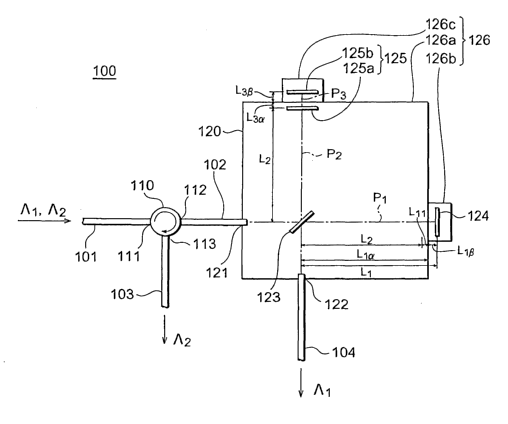
An optical filter 120 and an interleaves 100
8
CA 02462844 2004-04-02
FP02-0155-00
including the filter will now be described as an
embodiment of the temperature-compensated optical
communication interference device according to the
present invention. Fig. 1 is a schematic plan view
showing a configuration of the interleaver 100 and the
optical filter 120. The interleaver 100 consists of a
circulator 110 and the optical filter 120.
The optical circulator 110 has a first terminal
111, a second terminal 112, and a third terminal 113.
When light enters the first terminal 111 through
optical fiber 101, the optical circulator 110 feeds. the
light through the second terminal 112 into optical
fiber 102. When light enters the second terminal 112
through the optical fiber 102, the optical circulator
110 feeds the light through the third terminal 113 into
optical fiber 103.
The optical filter 120 has a first port 121, a
second port 122, a beam splitter 123, a first mirror
124, a second mirror 125, and a substrate 126. The
first port 121 is coupled to the second terminal 112 of
the optical circulator 110 through the optical fiber
102. The beam splitter 123 is, for example, a half
mirror.
The first port 121, second port 122, beam
splitter 123, first mirror 124, and second mirror 125
constitute a Michelson interferometer. The mirrors 124
9
CA 02462844 2004-04-02
FP02-0155-00
and 125 are optical components for reflecting light.
The beam splitter 123 serves as both an optical divider
and an optical coupler. When the beam splitter 123
receives light from the first port 121, it divides the
light into two beams. The beam splitter 123 directs
one divided beam toward the first mirror 124 and
directs the other divided beam toward the second mirror
125. These divided beams are reflected by the first
and second mirrors 124, 125, respectively, and then
return to the beam sp utter 123. The beam splitter 123
divides the light reflected by the first mirror 124,
into two beams, and directs one divided beam toward the
first port 121 and the other divided beam toward the
second port 122. The beam splitter 123 also divides
the light reflected by the second mirror 125, into two
beams and directs one divided beam toward the first
port 121 and the other divided beam toward the second
port 122.
The second mirror 125 is a Gires-Tournois
resonator including a half mirror 125a with the
transmittance of several ten o and a total reflection
mirror 125b. The half mirror 125a and the total
reflection mirror 125b are parallel to each other. The
half mirror 125a reflects part of the light from the
beam splitter 123 and transmits the rest part. The
transmitted light travels toward the total reflection
CA 02462844 2004-04-02
FP02-0155-00
mirror 125b. The total reflection mirror 125b reflects
the transmitted light toward the half mirror 125a. The
half mirror 125a and the total reflection mirror 125b
repeatedly reflect the light from the beam splitter 123
in this way between them. Part of this light passes
through the half mirror 125a and returns to the beam
splitter 123. As a result, the reflection
characteristic of the second mirror 125 has wavelength
dependence. The reflectance of the second mirror 125
periodically changes between Oo and 100 according to
the wavelength. The period of change of reflectance
(wavelength spacing) is determined by the optical
distance between the half mirror 125a and the total
reflection mirror 125b.
The substrate 126 is provided for fixing the
first port 121, the second port 122, the beam splitter
123, the first mirror 124, and the second mirror 125
thereto. The substrate 126 has a main member 126a, a
first mirror support member 126b, and a second mirror
support member 126c. Coefficients of linear expansion
of the respective mirror support members 126b and 126c
have a sign different from that of a coefficient of
linear expansion of the main member 126a. The first
port 121, second port 122, beam splitter 123, and half
mirror 125a are fixed on the main member 126a. The
first mirror 124 is fixed on the first mirror support
11
CA 02462844 2004-04-02
FP02-0155-00
member 126b. The total reflection mirror 125b is fixed
on the second mirror support member 126c.
Hereinafter, let the first optical path P1 be an
optical path in which one of the two divided beams by
the beam splitter 123 travels to the first mirror 124
and then reflected thereby back to the beam splitter
123, and L1 be the optical path length between the beam
splitter 123 and the first mirror 124. Furthermore,
let the second optical path P2 be an optical path in
which the other of the two divided beams by the beam
splitter 123 travels to the second mirror 125 and then
reflected thereby back to the beam splitter 123, and Lz
be the optical path length between the beam splitter
123 and the half mirror 125a. The beam splitter 123 is
positioned at one end of the first optical path P1 and
the first mirror 124 at the other end thereof. The
beam splitter 123 is positioned at one end of the
second optical path P2 and the second mirror 125 at the
other end thereof. In the present embodiment, L1 > L2.
In addition, let a be the coefficient of linear
expansion of the main member 126a, ail be the
coefficient of linear expansion of the first mirror
support member 126b, and biz be the coefficient of
linear expansion of the second mirror support member
126c. The signs of oc and ail are different. The signs
of a and (32 are also different. The signs of (31 and (32
12
CA 02462844 2004-04-02
FP02-0155-00
are the same.
With respect to the first optical path P1, the
part extending along the optical path length Lla = (L2 +
L11) from the beam splitter 123 is located above the
main member 126a, and the rest part with the path
length Llp above the first mirror support member 126b.
As for the second optical path P2 on the other hand,
the whole part with the path length LZ is located above
the main member 126a.
The sizes of the main member 126a and the mirror
support member 126b are preferably determined so as to
satisfy the following relations.
L1 = L2 + L11 + Llp (1a)
a'Lii + ~1'Llp = 0 (1b)
If the temperature changes by DT, the length of
the first optical path P1 will change from initial L1
to the following L1':
Ll' - (L2 + Lii) (1 + a0T) + Llp(1 + ~31~T) (2)
On the other hand, if the temperature changes by DT,
the length of the second optical path P2 will change
from initial Lz to the following LZ':
L2' - Lz (1 + a~T) (3)
Therefore, the optical path length difference DL' with
the change of temperature by DT is expressed by the
following equation in consideration of above Eqs (la)
and (1b)
13
CA 02462844 2004-04-02
FP02-0155-00
DL' - L1' - Lz'
- L11 ( 1 + a~T ) + L1R ( 1 + (31~T )
- Lii + Lip + (a~Lm + ~WLip) DT
- L11 + Llp
- L1 - Lz (4)
This is equal to the optical path length difference
before the change of temperature. Thus the temperature
dependence of the optical path length difference
between the first and second paths P1 and Pz is reduced
due to the difference in the signs of the coefficients
of linear expansion between the main member 126a and
the first mirror support member 126b.
More generally, the sizes of the main member 126a
and the mirror support member 126b are preferably
determined so as to satisfy the following relations.
Li = Li« + Lip ( 5a )
(Li« - Lz) -a + Llayl = 0 (5b)
In these equations, L1« represents the optical path
length of the part located above the main member 126a
in the first optical path P1, and Llp the optical path
length of the part located above the first mirror
support member 126b in the first optical path P1.
If the temperature changes by DT, the length of
the first optical path P1 will change from initial L1
to the following L1':
L1' - Ll« (1 + a0T) + Llp (1 + (31~T)
14
CA 02462844 2004-04-02
FP02-0155-00
On the other hand, if the temperature changes by DT,
the length of the second optical path PZ will change
from initial L2 to the following LZ':
L2' - Lz ( 1 + a~T ) ( 7 )
Accordingly, the optical path length difference DL'
with the change of temperature by DT is expressed by
the following equation in consideration of above Eqs
(5a) and (5b):
DL' - I L1' - L2' I
- ILla(1 + a~T) + Lla(1 + (31~T) - L2 (1 + a~T) I
- I (L1a - L2) (1 + a~T) + L1R (1 + (31~T) I
- I (L~a + Ly - L2) + ~ (Lza - L2) 'a + L1R' ~1) ~'I' I
- ILK - L21 (8)
This is equal to the optical path length difference
before the change of temperature. When the sizes of
the main member 126a and the mirror support member 126b
are determined so as to satisfy Eqs (5a) and (5b) as
described above, the temperature dependence of the
optical path length difference between the first and
second paths P1 and P2 is reduced. In practice, it is
feasible to adequately reduce the temperature
dependence of the path length difference between P1 and
P2 if the following relation is met instead of above Eq
(5b) .
-0.1 <- (Lla - LZ) 'a + Llp' (31 <_ 0.1 (9)
With respect to the optical path P3 between the
CA 02462844 2004-04-02
FP02-0155-00
half mirror 125a and the total reflection mirror 125b,
the part extending along the optical path length L3a
from the half mirror 125a is located above the main
member 126a, and the rest part with the path length L3R
above the second mirror support member 126c. The half
mirror 125a is positioned at one end of the third
optical path P3, and the total reflection mirror 125b
at the other end thereof. The half mirror 125a is also
located at one end of the second optical path P2. The
sizes of the main member 126a and the second mirror
support member 126c are preferably determined so as to
satisfy the following relation.
a'L3a + ~z'Lsp = ~ (10)
The temperature dependence of the optical path length
between the half mirror 125a and the total reflection
mirror 125b is reduced due to the difference in the
signs of the coefficients of linear expansion between
the main member 126a and the second mirror support
member 126c. In practice, it is feasible to adequately
reduce the temperature dependence of the optical path
length between the half mirror 125a and the total
reflection mirror 125b if the following relation is met
instead of above Eq (10).
-0.1 ~ Oc'L3a + (32~L3p _< 0.1 (11)
Referring to Figs. 2-4, the fixing structure for
the beam splitter 123 will now be described. Figs. 2
16
CA 02462844 2004-04-02
FP02-0155-00
to 4 are a plan view, a front view, and a side view
showing the fixing structure. The beam splatter 123 is
fixed to the main member 126a of the substrate using a
housing 20 as a fixing member. In this embodiment, the
beam splatter 123 is shaped in a regular quadrangular
prism. It is, however, noted that the shape of the
beam splatter 123 is not limited to this shape. The
main member 126a is made of a metal material, e.g.
stainless steel like SUS304. The housing 20 is also
made of a metal material, e.g. stainless steel like
SUS304. The housing 20 is joined to the main member
126a by welding. The housing 20 has a bottom portion
21, and vertical wall portions 23 and 25. The bottom
portion 21 is in contact with the upper surface of the
main member 126a. The vertical wall portions 23 and 25
stand upright from the both end portions of the bottom
portion 21 in the direction intersecting with the
substrate 126.
The angle between the bottom portion 21 and the
vertical wall portion 23 is equal to the angle between
two adjacent side faces of the beam splatter 123, and
is 90° in this embodiment. This permits the beam
splatter 123 to be positioned by placing two continuous
side faces 123b and 123d of the beam splatter 123
against a corner portion 27 formed by the bottom
portion 21 and the vertical wall portion 23.
17
CA 02462844 2004-04-02
FP02-0155-00
In the case where the beam splitter 123 is of
polygonal shape, the number of faces of the beam
splitter 123 in contact with the housing 20 may be one,
or three or more. In the case where the beam splitter
123 is of cylindrical shape, the beam splitter can be
positioned when a portion of the peripheral part
(circumferential part) of the beam splitter 123 or two
points spaced from each other on the peripheral part
are in contact with the housing 20.
The beam splitter 123 is fixed to the housing 20
by biasing forces of springs 31, 33 placed between the
beam splitter 123 and the housing 20. The springs 31,
33 are made of a metal material, e.g. stainless steel.
The springs 31, 33 are leaf springs. It can also be,
however, contemplated that the springs 31, 33 are
springs other than the leaf springs, e.g. coil springs.
The spring 31 is placed between one side face
123a of the beam splitter 123 and the vertical wall
portion 25. The side face 123a in contact with the
spring 31 is located on the opposite side of the side
face 123b in contact with the vertical wall portion 23.
The two ends 31a of the spring 31 are in contact with
the vertical wall portion 25. The central portion 31b
of the spring 31 is in contact with the side face 123a
of the beam splitter to bias the beam sp utter 123.
The side face 123a is located on the opposite side of
18
CA 02462844 2004-04-02
FP02-0155-00
the face 123b of the beam splatter 123 in contact with
the vertical wall portion 23. The beam splatter 123 is
pressed against the vertical wall portion 23 by the
biasing force of the spring 31.
The spring 33 extends between catching portions
23a and 25a provided in the respective vertical wall
portions 23 and 25. The two ends of the spring 33 are
caught by the catching portions 23a and 25a. The
central part of the spring 33 is in contact with upper
surface 123c of the beam splatter to bias the beam
splatter 123. The upper surface 123c is located on the
opposite side of the surface 123d of the beam splatter
123 in contact with the bottom portion 21. The beam
splatter 123 is pressed against the bottom portion 21
by the biasing force of the spring 33.
Thus the beam splatter 123 is pressed against the
housing 20 by the springs 31 and 33 so that the corner
portion 123e thereof fits the corner portion 27 of the
housing 20. This permits the beam splatter 123 to be
securely fixed to the housing 20.
The biasing forces of the springs 31, 33 act on
the faces except for a light receiving face 123f and
light emitting face 1238 of the beam splatter 123.
This permits the beam splatter 123 to be fixed to the
housing 20 without deteriorating the optical function
of the beam splatter 123.
19
CA 02462844 2004-04-02
FP02-0155-00
The biasing forces of the springs 31, 33 are set
at values within the range in which the optical
characteristics of the beam splitter 123 are not
affected. This permits the beam splitter 123 to be
fixed to the housing 20 without deteriorating the
optical function of the beam splitter 123.
A method of fixing the beam sputter 123 will now
be described. First, the beam splitter 123 is biased
by the springs 31, 33 to be fixed to the housing 20.
The spring 31 is brought into contact with the side
face 123a of the beam splitter 123 and the spring 33 is
brought into contact with the upper surface 123c of the
beam splitter 123. This results in pressing the beam
splitter 123 against the housing 20 so that the corner
portion 123e of the beam splitter 123 fits the corner
portion 27 of the housing 20. The beam splitter 123 is
fixed to the housing 20 in this way.
Then the housing 20 with the beam splitter 123
fixed thereto is positioned on the main member 126a and
thereafter the housing 20 is welded to the main member
126a. Welding is better than bonding. After the
housing 20 is welded to the main member 126a, the
housing 20 rarely moves even when change of temperature
occurs. Therefore, the temperature dependence of the
optical path lengths L1, Lz is suppressed. If the
housing 20 were bonded contrary, an adhesive would
CA 02462844 2004-04-02
FP02-0155-00
contract with temperature change and thus the housing
20 would move. The amount of the movement must be
greater than that in the case of welding. Thus the
optical path lengths L1, L2 would be easier to change
depending on the temperature if the housing 20 were
bonded.
The housing 20 and the main member 126a are
preferably welded with each other using a YAG laser
beam. The weld time can be extremely short in the YAG
laser welding operation. When they are welded by the
YAG laser welding, the housing 20 moves because of
impact. However, this motion is normally smaller than
the motion due to curing and contraction of the resin
adhesive.
The conditions for the YAG laser welding, for
example, the strength of the YAG laser beams and
positions at which the beams are irradiated, are
properly determined according to the materials and
shapes of the housing 20 and the main member 126a in
consideration of the movement of the housing 20 due to
the impact during the welding operation. In stead of
the YAG laser welding, other laser welding such as
carbon dioxide laser welding or the like may also be
used.
The housing is preferably welded at least at two
points by the YAG laser welding. This permits the
21
CA 02462844 2004-04-02
FP02-0155-00
housing 20 to be fixed more securely to the main member
126a. When the YAG laser welding is carried out at two
or more points by a plurality of separate operations,
it is feasible to correct the positional deviation
caused by the first YAG laser welding operation by the
second or later YAG laser welding operation.
In the present embodiment, the half mirror 125a
is also fixed on the main member 126a using a fixing
structure similar to that for the beam splitter 123.
Therefore, the half mirror 125a also produces little
positional deviation with the temperature change. This
further suppresses the temperature dependence of the
optical path length L2.
The interleaver 100 operates as follows. Light
propagating in the optical fiber 101 enters the first
terminal 111 of the optical circulator 110 and goes out
from the second terminal 112. The light travels
through the optical fiber 102 and the first port 121
into the optical filter 120. The input light is
divided into two beams by the beam splitter 123. One
divided beam is fed into the first optical path P1 and
the other divided beam is fed into the second optical
path P2.
The beam fed into the first optical path P1 by
the beam splitter 123 travels forward and backward
between the beam splitter 123 and the first mirror 124,
22
CA 02462844 2004-04-02
FP02-0155-00
and returns to the beam splitter 123 to be divided into
two beams. One divided beam travels to the first port
121 and the other divided beam to the second port 122.
The beam fed into the second optical path P2 by
the beam splitter 123 travels forward and backward
between the beam splitter 123 and the second mirror
125, and returns to the beam splitter 123 to be divided
into two beams. One divided beam travels to the first
port 121 and the other divided beam to the second port
122.
On the optical path between the first port 121
and the beam splitter 123, part of the light from the
first optical path P1 is superposed on part of the
light from the second optical path P2 to effect
interference with each other. The superposed light
travels through the first port 121 and the optical
fiber 102 into the second terminal 112 of the optical
circulator 110. Thereafter, the superposed light
travels through the third terminal 113 into the optical
fiber 103.
Likewise, on the optical path between the second
port 122 and the beam splitter 123, part of the light
from the first optical path P1 is superposed on part of
the light from the second optical path PZ to effect
interference with each other. The superposed light
travels through the second port 122 into the optical
23
CA 02462844 2004-04-02
FP02-0155-00
fiber 104.
As described above, the second mirror 125
constitutes a Gires-Tournois resonator and the
reflection characteristic thereof has wavelength
dependence. Therefore, the interleaver 100 is able to
receive and demultiplex signal light of multiple
wavelengths (?~1, 1~2, . . . , 1~z"-1, 1~2n, . . - ) from the optical
fiber 101 to output signal light of a first wavelength
group 111 (?~1, ~3, . . . , ~za-i. . . . ) into the optical fiber
104 and signal light of a second wavelength group l~z
(l~z, 1~9, . . . , 1~2", . . . ) into the optical fiber 103 . The
wavelengths herein satisfy the relation of 1~1 < ?,z
< . . . < ~lzn-1 < ~2n < . . . The wavelength spacing of the
multi-wavelength signal light is determined by the
optical distance between the half mirror 125a and the
total reflection mirror 125b.
In the interleaves 100, as described previously,
the temperature dependence of the optical path length
difference (L11 + L1R) between the first optical path P1
and the second optical path Pz is reduced. The
temperature dependence of the optical path length (L3«
+ L3R) between the half mirror 125a and the total
reflection mirror 125b is also reduced. Accordingly,
the temperature dependence of the transmittance is
reduced for each of the light of the first wavelength
group 111 and the light of the second wavelength group
24
CA 02462844 2004-04-02
FP02-0155-00
A2. Namely, the transmission characteristic (the
relation between the wavelength and transmittance) of
the interleaver 100 has reduced temperature dependence.
Since there is no need for a temperature adjusting
means to maintain the temperature constant, the
interleaver 100 can be constructed in small size.
A specific example of the interleaver 100
according to the present embodiment will now be
described. The example provides the interleaver 100
for demultiplexing multi-wavelength signal light with
the frequency spacing of 100 GHz. Since the Free
Spectral Range (FSR) is 100 GHz, the path length
difference (L11 + Llp) between the first optical path P1
and the second optical path P2 is 1.498570 mm. The
main member 126a is made of stainless steel SUS304.
The coefficient of linear expansion a of the main
member 126a is 1.73 x 10⁻⁵. The first and second mirror
support members 126b, 126c are made of a ceramic
material of CERSAT (trade mark) available from Nippon
Electric Glass Co., Ltd. The coefficients of linear
expansion thereof (31 and (32 are -8.2 x IO-6. According
to the above Eq (1b), the optical path length L11 is
0.4819 mm and the optical path length Llp 1.01667 mm.
An optical communication system 1 according to
the present embodiment will now be described. Fig. 5
is a schematic illustration showing a configuration of
.. 2 5
CA 02462844 2004-04-02
FP02-0155-00
the optical communication system 1. The optical
communication system 1 comprises optical transmitters
11 and 12, a multiplexing interleaver 20, an optical
fiber transmission line 30, a demultiplexing
interleaver 40, and optical receivers 51 and 52. The
multiplexing interleaver 20 and the demultiplexing
interleaver 40 have the same structure as the
interleaver 100 described above. Accordingly, the
temperature dependence of optical transmission
characteristics of the interleavers 20 and 40 is
reduced.
The optical transmitter 11 outputs multiplexed
signal light of the first wavelength group 111
~s. . . . . ~zn-i. . . . ) . The optical transmitter 12 outputs
multiplexed signal light of the second wavelength group
nz (~z. ~4. . . .. ~zn. . . . ) . The first wavelength group 111
includes only odd channels, and the second wavelength
group 112 only even channels. The multiplexing
interleaver 20 receives the multi-wavelength signal
light of the first wavelength group 111 from the optical
transmitter 11 and also receives the multi-wavelength
signal light of the second wavelength group 1~2 from the
optical transmitter 12. The multiplexing interleaver
20 multiplexes these signal light and feeds the
multiplexed light into the optical fiber transmission
line 30. The demultiplexing interleaver 40 receives
26
CA 02462844 2004-04-02
FP02-0155-00
the multiplexed signal light through the optical fiber
transmission line 30. The demultiplexing interleaves
40 demultiplexes the multiplexed signal light into the
multi-wavelength signal light of the first wavelength
group n1 and the multi-wavelength signal light of the
second wavelength group n2. The demultiplexing
interleaves 40 sends the signal light of the first
wavelength group n1 to the optical receiver 51 and also
sends the signal light of the second wavelength group
A2 to the optical receiver 52. The optical receiver 51
demultiplexes the signal light of the first wavelength
group n1 to individually receive signal lightwaves of
the respective wavelengths included in the first
wavelength group n1. The optical receiver 52
demultiplexes the signal light of the second wavelength
group n2 to individually receive signal lightwaves of
the respective wavelengths included in the second
wavelength group A2.
In the optical communication system 1, as
described above, the temperature dependence of the
optical transmission characteristic is reduced for each
of the multiplexing interleaves 20 and the
demultiplexing interleaves 40. Accordingly, the
temperature dependence of transmission quality of
signal light is also reduced in the optical
communication system 1.
27
CA 02462844 2004-04-02
FP02-0155-00
The present invention is not limited to the above
embodiments, but can be modified in various ways. For
example, the temperature-compensated optical
communication interference device according to the
present invention may be any other optical component,
without having to be limited to the interleaver or the
optical filter. The temperature-compensated optical
communication interference device according to the
present invention does not always have to be the
Michelson interferometer type optical device described
above, but may also be, for example, a Mach-Zehnder
interferometer type optical device.
In the above embodiment, the first mirror 124 and
the total reflection mirror 125b are fixed on the
separate members 126b and 126c, respectively.
Alternatively, these mirrors 124 and 125b may be fixed
on the same member.
Fig. 6 is a schematic plan view showing an
interleaver 100a in which the first mirror 124 and the
total reflection mirror 125b are fixed on an L-shaped
mirror support member 126d. The L-shaped member 126d
is joined to two adjacent sides of the main member
126a. The other structure of the interleaver 100a and
the optical filter 120a is the same as that of the
interleaver 100 and the optical fiber 120 shown in Fig.
1. Redundant description is omitted herein
28
CA 02462844 2004-04-02
FP02-0155-00
accordingly.
In the following, let a be the coefficient of
linear expansion of the main member 126a, and (33 be the
coefficient of linear expansion of the L-shaped member
126d. The signs of a and ~i3 are different.
With respect to the first optical path P1, the
portion extending along the optical path length L1« -
(LZ + L11) from the beam splitter 123 is located above
the main member 126a, and the rest part with the
optical path length Llp above the L-shaped member 126d.
As for the second optical path P2, on the other hand,
the whole part with the optical path length Lz is
located above the main member 126a. With respect to
the optical path P3 between the half mirror 125a and
the total reflection mirror 125b, the portion extending
along the optical path length L3« from the half mirror
125a is located above the main member 126a, and the
rest part with the optical path length L3p above the L-
shaped support member 126d.
The sizes of the main member 126a and the L-
shaped member 126d are preferably determined so as to
satisfy the following relations:
Ll = L1« + L1 R ( 11 a )
(Li« - Lz) ~a + Llp~[33 = 0 (11b)
a~L3« + (33~L3a = 0 (11c)
Eqs (11b) and (11c) correspond to Eqs (5b) and (10) for
29
CA 02462844 2004-04-02
FP02-0155-00
the interleaver 100 shown in Fig. 1.
When the sizes of the main member 126a and the L-
shaped member 126d. are determined so as to satisfy Eqs
(11a) and (11b), the temperature dependence of the
optical path length difference between the first
optical path P1 and the second optical path P2 is
reduced. In practice, it is feasible to adequately
reduce the temperature dependence of the optical path
length difference between P1 and P2 if the following
relation is met instead of above Eq (11b):
-0.1 -<< (Lla - L2) '(x + Llp'(33 ~ 0.1 (12)
When the sizes of the main member 126a and the L-
shaped member 126d are determined so as to satisfy Eq
(11c), the temperature dependence of the optical path
length between the half mirror 125a and the total
reflection mirror 125b is reduced. In practice, it is
feasible to adequately reduce the temperature
dependence of the optical path length between the half
mirror 125a and the total reflection mirror 125b if the
following relation is met instead of above Eq (11c):
-0.1 ~ cx'L3a + (33'L3p <- 0.1 (13)
In the interleaver 100a, the first mirror 124 and
the half mirror 125a are fixed to the single member
126d. Therefore, the interleaver 100a can be
fabricated by the smaller number of steps than the
interleaver 100 in which the first mirror 124 and the
CA 02462844 2004-04-02
FP02-0155-00
half mirror 125a are separately fixed to the first and
second members 126b and 126c.
In the above embodiments, the beam splitter 123
and the first mirror 124 are placed separately between
the members with the coefficients of linear expansion
having different signs. However, in the present
invention, optical coupler, optical divider and optical
components may be placed one or more members with
coefficients of linear expansion having the same sign.
Even in this case, it is possible to cancel out the
changes, according to temperature change, in the
lengths of the first and second optical paths, thereby
reducing the temperature dependence of the optical path
length difference between these two paths if at least
one of these paths extends above both of the members
with the coefficients of different signs. This is
realized, for example, by placing the optical coupler,
optical divider and optical components separately on
the members with either positive or negative
coefficients and interposing a member with the
coefficient of the opposite sign between these members.
Industrial Applicability
The present invention is able to cancel out the
changes, according to temperature change, in the
lengths of the first and second optical paths, and
suppress the change in the optical path length
31
CA 02462844 2004-04-02
FP02-0155-00
difference. Consequently, the invention can provide
the interference device with reduced temperature
dependence of the transmission characteristic, and also
the optical transmission system with reduced
temperature dependence of the characteristic of
transmitting the signal light.
32