Note: Descriptions are shown in the official language in which they were submitted.
CA 02463015 2004-04-O1
a
2003P04986US-pre
Patent-Treuhand-Gesellschaft
fur elektrische Gliihlampen mbH., Munich
Method for varying the power consumption of capacitive
loads
TECHNICAL FIELD
The invention relates to a method and a control circuit
for varying the power consumption of capacitive loads,
which are operated on the AC voltage power supply
system by connecting and disconnecting, at the system
frequency, the system power supply in each system half-
cycle, and in particular to a ballast for a lamp.
BACKGROUND ART
Lamps such as discharge lamps, in particular compact
fluorescent lamps (CFL), are usually operated on the
power supply system by means of a rectifier circuit for
rectifying an AC voltage supply and charging a
capacitor, which is often referred to as a smoothing
capacitor. The term lamp used here relates in
particular to the compact fluorescent lamps mentioned,
but may also be understood to mean other lamps such as
halogen lamps. The DC voltage present across the
capacitor serves the purpose of supplying power to an
inverter, which operates the compact fluorescent lamp.
The invention generally relates to varying the power
consumption of capacitive loads, the term "capacitive"
in the case of lamp circuits meaning the so-called
smoothing capacitor at the input of the inverter.
CA 02463015 2004-04-O1
2
DISCLOSURE OF THE INVENTION
One object of the present invention is to specify an
improved method and an improved control circuit for
varying the power consumption of capacitive loads.
For this purpose, the invention provides a method for
varying the power consumption of loads having a
capacitive input on an AC voltage power supply system
by connecting and disconnecting, at the system
frequency, in each system half-cycle the system power
supply, in that, as long as the system power supply is
disconnected, a current path bridging the load inputs
is created, and in that, when the system power supply
is connected, a smoothing capacitor is charged by means
of a converter until the voltage across the smoothing
capacitor of the load reaches a predetermined maximum
value. Converters will be understood below to mean
devices which are suitable for converting an input
voltage into an output voltage having a different time
characteristic. In particular, these converters may be
step-down converters or inverse converters or step-up
converters.
The invention particularly relates to a circuit for
carrying out said method and to an electronic ballast
for a compact fluorescent lamp having such a circuit
for operation using a phase-gating dimmer.
The inventors have used as a basis the knowledge that
the possibilities for dimming or regulating the power
in the case of capacitive loads are in need of
improvement. When the system power supply is not
constant, such as during dimming, for example,
capacitive loads such as compact fluorescent lamps are
susceptible to instabilities which appear in the form
of disruptive flickering in the case of lamp operation.
CA 02463015 2004-04-O1
3
It is true that, in the past, various pump circuits
(known as circuits for reducing the line current
harmonic components) have been used which allow for
longer current flow angles, i.e. for the current to be
drawn constantly, and thus improved dimming properties.
However, such pump circuits require a large number of
components. One disadvantage is the fact that the known
pump circuits need to be designed such that, when the
lamps are operated without dimmers, the line current
harmonic components which occur do not exceed the
relevant limit values. Tn addition, the pumping power
of such pump circuits depends on the instantaneous
voltage of the rectifier voltage int~srmediate circuit,
as a result of which asymmetries of the dimmer result
between successive system half-cycles, which result in
the operated lamp flickering. In addition, no provision
is made to ensure that the mentioned pumping power is
kept at a sufficiently high value and, when operating
using a dimmer, the smoothing capacitor is not
recharged suddenly with high current peaks when the
power breaker of the dimmer (triac) is closed, which
can ultimately have negative effects on the life of the
lamp.
The basic concept of the invention is to eliminate the
mentioned instabilities and effects. For this purpose,
in a first phase, in which the system power supply is
disconnected, the method according to the invention,
which relates in particular to the operation of
capacitive loads using phase-gating dimmers, isolates a
current path which bridges the inputs of the load.
"Bridging" or '°short-circuiting" is intended to mean
that bridging occurs at least for low-frequency input
voltages. Low-frequency means that, at such an input-
voltage frequency, the inductive z:esistance in the
converter (inductor) needs to be negligible compared
with the timing resistance set in the dimmer. This low-
resistance current path makes it possible to then
charge, for example, the timing element of the power
CA 02463015 2004-04-O1
4
breaker in a dimmer even when no power is being
supplied to the load. Once the system power supply has
been connected, a converter operates until the voltage
across the smoothing capacitor of the load reaches a
predetermined maximum value. This makes it possible to
prevent the smoothing capacitor of the lamp from being
overloaded. The current path of the converter is in
this case preferably designed such that on average over
time the current is at least as great as the level of
the holding current required for maintaining the system
power supply.
One variant of the method provides for the
predetermined maximum value for the voltage across the
smoothing capacitor to be reduced when the time at
which the system power supply is in each case connected
falls below a predetermined minimum value. This has the
advantage, in particular when operating using phase-
gating dimmers, that, in the event of very high phase-
gating angles, reactive currents and losses in the
current-carrying components can be reduced.
The method according to the invention preferably
detects, in a further step, whether the load is
operated using a dimmer or whether it has a continuous
system power supply. Continuous means that the AC
voltage is applied to the input of the load permanently
and constantly. For this purpose, tl~e current path is
permanently disconnected, i.e. the converter operation
is deactivated.
The method according to the invention is carried out by
a circuit according to the invention. This circuit has
at least one current path which cart be connected and
disconnected and which bridges the inputs of the load.
It is thus possible according to t he invention, for
example in the case of dimmer operation, for the dimmer
timing element to be charged even when there is no
power breaker (triac in the dimmer) connected. A
CA 02463015 2004-04-O1
control element is also provided which ensures that the
voltage across the capacitive input. of the load is
detected and the current path is connected and
disconnected accordingly. The detection preferably
takes place by an image of the system voltage being
produced by means of three resistors on the system side
of the load upstream of a rectifier.
In addition, the circuit can evaluate a signal of the
system power supply and produce a control signal on the
basis of this signal which controls the power
consumption of the load. This makes it possible to
match the load operation to the variable system power
supply.
In the present invention, the preferred form of the
converter is a step-up converter. The current path in
the circuit is preferably formed by a transistor which
can be controlled by the control element. The step-up
converter operates according to the invention once the
system power supply has been applied to the load until
the voltage across the smoothing capacitor of the load
reaches a predetermined maximum value. This makes it
possible to prevent overvoltages across the smoothing
capacitor of the load, and for the life of the lamp
overall to be positively influenced. In order to
further reduce disruptive effects (for example the
inductor of the dimmer), provision is made for the
inputs of the load to be short-circuited upstream of
the converter, thus bypassing the converter. This takes
place according to the invention by means of an
interface circuit which is connected between the
rectifier and the converter and which produces a short
circuit as long as no power is being supplied to the
load on the system side. The interface circuit is in
this case preferably decoupled from the converter by
means of a decoupling diode such that no discharge
processes can take place via the interface circuit,
starting from the converter.
CA 02463015 2004-04-O1
6
BRIEF DESCRIPTION OF THE DRAWINGS
The invention will be explained in more detail below
with reference to several exemplary embodiments. In the
drawing:
figure 1 shows a circuit arrangement for the operation
of a load using a phase-gating dimmer;
figure 2 shows an example of a circuit arrangement for
realizing the method according to the
invention;
figure 3 shows a diagram which shows,, as a function of
time, a) the qualitative characteristic of
the system voltage provided by the phase-
gating dimmer, b) the qualitative
characteristic of the voltage above that of
the load, and c) the characteristic of the
voltage signal at the control input of the
transistor which is operated as a switch in
the step-up converter;
figure 4 shows a further diagram which shows similar
time characteristics of the variables
mentioned in figure 3;
figure 5a shows an exemplary circuit: for implementing
the method according to the invention;
figure 5b shows a further exemplary circuit for
implementing the method according to the
invention;
figure 6 shows a diagram which shows the
characteristic of an output voltage used to
regulate the power consumption of the load as
CA 02463015 2004-04-O1
7
a function of the phase-gating angle set in
the phase-gating dimmer; and
figure 7 shows a circuit diagram of a circuit
according to the invention having ~an
integrated interface circuit.
BEST MODE CARRYING OUT THE TNVENTION
Figure 1 shows an example of the circuit arrangement
for the operation of a load using a phase-gating
dimmer. Shown is a circuit in which a load CFL is
operated by an AC voltage/system power supply VS. The
load CFL is supplied with power by this voltage source
VS via a phase-gating dimmer (between the points N and
P). Phase-gating dimmers provide a periodic system
power supply to the load which is isolated in each
half-period, with a time delay, by tripping a power
breaker triac by means of a variable timing element
diac, TR, TC. In addition to the power breaker triac
and the timing element, which is formed from a diac, a
capacitor TC and a variable resistor TR, there are
generally further provided in the dimmer circuit a fuse
F and, for radio interference suppression, also a
capacitor C and an inductor L.
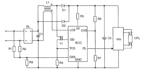
The method according to the invention is based on the
arrangement in terms of circuitry of a step-up
converter which is formed in figure 2 as part of the
integrated ballast of a compact fluorescent lamp (CFL)
by the capacitor C1, the capacitor C2, the diode Dl,
the inductor L1 and the switch in the form of a
transistor T1. The compact fluorescent lamp contains a
rectifier GL, by means of which the capacitor C2 (i.e.
the capacitive input of the load) is charged via the
inductor L1. The capacitor C2 supplies power to a lamp
CFL via an inverter circuit INV mentioned initially. A
control circuit BCC is used to supply power to the
CA 02463015 2004-04-O1
capacitor C2 via the transistor T1 by driving the
output GD.
The circuit operates as follows: The system AC voltage
is converted in the rectifier GL to a pulsating DC
voltage. The primary winding of an inductor L1 is
connected in series with an additional secondary
winding in the positive lead wire. The secondary
winding can be used to detect the demagnetization of
the inductor L1.
When closed, the transistor T1 provides for an
increasing flow of current in the inductor L1 up to a
settable value which is measured using a resistor R4
which is connected in series with the transistor. The
current through T1 is detected by the control circuit
BCC as the voltage drop across R4 via the input TCS and
further processed.
Once the transistor T1 has opened, a diode D1 directs
the current injected into the inductor L1 into a
capacitor C2 until the inductor has completely
demagnetized. This demagnetization is detected by the
secondary winding on L1, which is connected to the
input LCS of the control circuit BCC.
According to the present invention, the control circuit
BCC which is described in more detail below controls,
via the output GD, the closing and opening of the
transistor Tl. This control circuit is supplied with
power, for example, via the resistor R5. Naturally,
other circuits for providing sufficient supply voltage
for the control circuit BCC may also be used.
The resistors R6 and R7 are used to detect the voltage
across the capacitor C2, and, divided in accordance
with the ratio R6/R7, this voltage is passed to the
input CVS of the control circuit BCC.
CA 02463015 2004-04-O1
9
The resistors Rl, R2 and R3 are connected such that,
for the purpose of detecting a phase-gating angle of
the system voltage being supplied, an image of the
instantaneously applied system voltage can be made
available to the control circuit BCC at the input DAS.
On the output side of the rectifier, the zero crossings
of the system voltage cannot be reliably detected owing
to any residual voltages across filter capacitors (Cl)
or parasitic capacitances (for example in GL) which may
be present. By connecting the two resistors R1 and R2
to the system side of the rectifier, the applied input
voltage, in particular its zero crossings, can be
detected independently of filter capacitors or radio
interference suppression capacitors.
Via the output DL, the control circuit BCC makes
available a signal, which is proportional- in size to a
phase-gating angle of a gated system voltage produced
by an external dimmer and detected via R1, R2 and R3 or
the input DAS. This signal may be used in a suitable
inverter (not described in any more detail here) for
controlling or regulating the lamp current and thus the
lamp brightness as a function of a phase-gating angle
set in the dimmer.
Reference is made to figure 3 to explain the further
operation of the circuit. Shown are the time
characteristics of the system voltage U(N) across the
resistor R3 (proportional to U(N)) which is provided by
the phase-gating dimmer; of the voltage across the
resistor R7 (proportional to U(C2)) or of the voltage
U(DAS) across the input DAS, which is an image of the
system voltage; and also of the voltage U(GD) present
across the output GD for driving the transistor T1.
At the end of a system half-cycle, the voltage across
the input DAS of the control circuit BCC becomes zero
(time t1). Then, BCC closes the transistor T1 by means
CA 02463015 2004-04-O1
of the output GD. In the phase ta, in which there is no
load current flowing through the transistor and thus
through the resistor R4, since the triac contained in
the dimmer which is present on the system side (cf.
figure 1) has not yet been closed (phase gating), the
transistor T1 remains permanently closed.
Owing to the closed transistor, the dimmable lamp
according to the invention appears to the dimmer to be
a low-resistance load such as an incandescent lamp, for
example. The capacitor TC of the timing element present
in the dimmer (formed by TR and TC, figure 1) can be
charged via the current path GL, L1, Tl and R4 by means
of the variable resistor TR of the timing element of
the dimmer until the triac is triggered by the diac,
although the lamp in the phase to does not itself
consume any power (charging current for the filter
capacitor). Only the small current which is required
for the operation of the timing element (TR, TC) in the
dimmer therefore flows during ta. Practically all of
the system voltage VS is present across the dimmer
(voltage P-N), almost in the form of a reverse voltage.
At the moment at which the triac is triggered in the
dimmer (time t2 ) , a current can flow through the dimmer
and the system voltage is applied to the input of the
dimmable CFL, and the voltage across the dimmer (P-N)
becomes almost zero. The physical properties of the
triac require a minimum current (so-called holding
current) to flow in order to keep the component in a
conducting state without further trigger pulses. If the
current value were to fall below this holding current,
the triac would be extinguished again, and, when the
internal timing element of the dimmer is set
accordingly, a renewed trigger pulse could be supplied
to the control input of the triac via the diac, as a
result of which a renewed flow of current would be
possible. This repeated triggering of the triac within
a system half-cycle results in clearly visible
CA 02463015 2004-04-O1
12
flickering of the lamp, particularly if the above-
described repeated triggering only takes place in every
second system half-cycle.
According to the invention, the proposed circuit
arrangement begins to operate at the 'time t2 as a known
step-up converter. The components L1, Tl and R4 are in
this case dimensioned such that the average current
drawn by the dimmable CFL at the time tb is greater
than the holding current for all triacs normally used
in dimmers . This prevents the triac in the dimmer from
being extinguished. At this time tb, the operation of
the circuit arrangement as a step-up converter results
in the smoothing capacitor C2 being charged, and the
voltage U C2 across C2 rises linearly.
At the time t3, the voltage U (CVS) which can be tapped
off at the voltage divider R6/R7 reaches a
predetermined maximum value U CVSmax. This maximum
value U,CVSmax results from the voltage level which can
be applied to the capacitor C2, the withstand voltage
of the switching elements contained in the inverter, a
divider ratio R6/R7, the operating point UDC4 or USUB
and the signal DL.
At this time t3, the operation of the circuit
arrangement in the form of a step-up converter is ended
according to the invention, the transistor T1 remains
permanently open 'antil the next zero crossing of the
system voltage, at which point a new cycle begins. In
this phase tc, the triac of the dimmer is extinguished,
but this no longer has any effect on the operation of
the CFL, since its smoothing capacitor C2 has been
charged to a sufficient voltage level and the inverter
arrangement INV or the lamp CFL can be supplied with
power.
The step-up converter operation means that the filter
capacitor is charged to the same value in each system
CA 02463015 2004-04-O1
12
half-cycle, even if asymmetries (slightly different
phase-gating angles for the positive and negative half-
cycle) occur in the dimmer. Flickering at a system-
voltage frequency can therefore not occur according to
the invention.
The invention may also be used if the load is operated
without a dimmer. In conventional circuits, in this
case the legal regulations with respect to the line
current harmonic components cannot be complied with.
This is because the step-up converter operation would
begin immediately after each system zero crossing (no
phase ta). The phase tb would then be complete so early
that, at a phase angle of 90°, no more current would
flow into the lamp. However, a corresponding standard
EN61000-3-2 prescribes a current flow beyond 90°.
The control circuit BCC according to the invention
detects whether a dimmer is present or whether the lamp
is operated directly on the power supply system.
Figure 4 schematically illustrates the transition into
operation of the lamp with deactivated step-up
converter, if no dimmer is present.
If no dimmer is present, the transistor T1 is,
according to the invention, no longer permanently
closed after a few system half-cycles (only the phase
tc is now carried out), for which reason a direct
capacitive charging current flows via the diode D2 from
the power supply system into the capacitor C2. The
dimensions of the capacitor must be the same as for the
nondimmable lamps which are today available in order to
comply with the abovementioned standard.
Figure 5 shows an example of one circuit arrangement
which implements the method according to the invention
and operates as follows.
CA 02463015 2004-04-O1
13
At the beginning of operation, the flipflops FFl and
FF2 are set such that their outputs Q1 and Q2 are logic
"one". The output of the comparator K3 is at the outset
likewise logic "one" since the capacitor contained in
AV1 has not yet been charged and there is thus no
voltage available as yet at the output of the low-pass
filter AVl.
These preconditions (G1E1=GlE2=G1E3=="one") mean that
the output GlA of the And gate Gl becomes logic "one",
the output GD of the control circuit is thus likewise
"one", and the transistor Tl is closed.
As a result of the current which starts to flow through
GL, L1, T1 and R4, the voltage across the input TCS,
and thus across the positive input of a comparator K1
now rises. As soon as the voltage across TCS exceeds
the predeterminable voltage DCl across the negative
input of K1, the output voltage of K1 rises sharply. By
means of a differentiator DIFFl, this rise is converted
into a short pulse which resets the flip-flop FF1 via
the input R1 of said flipflop FFl, and the output Q1
becomes "zero". This results, by means of the input
G1E1 of the And gate Gl, in the transistor T1 being
opened since GD likewise becomes °'zero". Alternatively,
it is possible to close the transistor T1 for a
predetermined time. In place of t:he comparator, a
corresponding timing circuit may be provided for this
purpose.
The demagnetization of the inductor L1 is detected via
the secondary winding on L1. The signal produced at
this secondary winding is supplied via the input LCS to
a differentiator DIFF2, at whose output a short pulse
is provided at the moment at which the current in L1
becomes zero. This short pulse resets the flipflop FF1
via the input S1 (Ql becomes "one"), which leads, by
means of G1 and GD, to the transistor T1. being closed
again.
CA 02463015 2004-04-O1
14
According to the invention, this above-described
operation of the circuit topology as a step-up
converter can be influenced by the two inputs GlE2 and
GlE3 of the And gate Gl such that the proposed method
can be carried out.
At the beginning of operation, the output Q2 of the
flipflop FF2 is at "one". As a result of the above-
described operation of the circuit topology as a step-
up converter (phase tb), the voltage across the
smoothing capacitor C2 and thus across the input CVS of
the control circuit rises.
If the voltage across CVS exceeds a predeterminable
value DC4, the output of the comparator K4 switches
from °'zero" to "one". This change in state is converted
by the differentiator DIFF4 into a short pulse which
resets the flipflop FF2 via the input: R2. As a result,
Q2 becomes °'zero", and the output o:~ the And gate G1
likewise becomes "zero" as G1E3=0. By means of G1E3 and
G1A, the transistor T1 remains reliably open (phase tc)
until the flipflop FF2 is reset (time t1).
If the voltage across the input DAS (which is
proportional to the voltage across the input of the
CFL) becomes smaller at the end of a system half-cycle
than a threshold voltage DC2 which can be set, the
output of the comparator K2 switches from "one" to
"zero". This change in state is converted by the
differentiator DIFF3 into a short pulse which resets
the flip-flop FF2 via the input S2. As a result, Q2
becomes "one", and the output of the And gate G1 can
now become "one" again with corresponding input
voltages across G2E1 and G1E2. The blocking of the gate
G1 via GlE3 which is required in phase tc is canceled
owing to the output Q2.
CA 02463015 2004-04-O1
The output signal of the comparator K'~ is also supplied
to a low-pass filter AV1, whose output voltage is thus
proportional to the phase-gating angle set in the
dimmer. The smoothed signal at the output of the low-
pass filter AVl is provided at the output DL of the
control circuit for the inverter INV in order to
achieve a desired luminous flux.
The comparator K3 detects whether the CFL is operated
using a dimmer. The voltage across 'the output of the
low-pass filter AVl is at a maximum when the entire
system voltage is present across the CFL. In this case,
the output voltage of AVl is greater than a
predeterminable threshold voltage DC:3, and the output
of the comparator is therefore "zero". Since the output
signal of K3 is applied at the input GlE2 of the And
gate G1, the output G1A of said And gate G1 is reliably
"zero", and the transistor Tl cannot be closed via G1
or GD.
Each dimmer has a minimum phase-gating angle, even if
it is set to 1000 brightness. As a result, the output
voltage of AV1 falls below the predeterminable value
DC3, as a result of which the output of K3 is "one°' . In
this state, the blocking of the gate Gl via G1E2 by
means of the output of K.3 is cance7_ed if the CFL is
operated using a dimmer.
In order to further improve the above-described method
for dimming CFLs, provision may be made for the
predeterminable maximum value U CVSmax for the voltage
across C2 to be slowly reduced at phase-gating angles
greater than a likewise predeterminable value. In this
case, account needs to be taken of the fact that a
direct recharging of C2 via the diode D2 fro~1 the power
supply system is reliably prevented. In each possible
operating state, the voltage across C2 needs to be
greater than the instantaneous value of the system
voltage.
CA 02463015 2004-04-O1
16
A corresponding exemplary circuit arrangement for the
control circuit is shown in figure 5b. Departing from
the previous embodiment with reference to figure 5a,
the comparator K4 is not supplied with a constant
comparison variable DC4 but with a voltage which
depends on the phase-gating angle (cf. figure 6).
In a subtractor SUB, a value which is dependent on the
set gating angle is subtracted from the maximum value
(predetermined by DC4) for the voltage across C2 at
phase-gating angles greater than a p~°edeterminable
value. The signal DL can be used for this purpose since
the output voltage of AVl falls at increasing gating
angles.
Figure 6 shows, by way of example, t:he output voltage
of the subtractor SUB as a function of the phase-gating
angle when the voltage across C2 is reduced at phase-
gating angles greater than 90°.
It is possible to determine the gating angle beyond
which the reference value U(SUB), supplied to the
comparator K4, for the maximum vo:Ltage U CVSmax is
reduced by varying the voltage DC4 and U(DL). The ratio
R6/R7 can then be used to set the actual maximum
voltage across C2. If, for example, the signal DC4 is
reduced, the voltage U(SUB) is reduced only at phase-
gating angles greater than 90°.
The above-described circuit arrangement should be
viewed only as an example of the technical realization
of the proposed method. Other circuits may also be used
with which the described method can be applied.
The timing element can also operate according to the
invention in the non-conducting state of the power
breaker in the dimmer (i.e. if no system voltage is
applied to the load). This means that the actual load
CA 02463015 2004-04-O1
17
is not present for the timing element when no power is
being supplied. The circuit arrangement according to
the invention in the load then represents a low-
resistance current path. The tripping process of the
power breaker in the dimmer is only defined by the
timing resistor TR and the timing capacitor TC (cf.
figure 1). It is thus possible to prevent, for example,
phase shifts from occurring which can shift the
tripping times in successive system half-cycles and can
ultimately lead to undesired flickering for the load.
According to the invention, a (sE:parate) interface
circuit may be connected upstream. of the step-up
converter. The interface circuit is designed such that
it bridges the transistor T1 and the inductor L1 in the
phase to such that the load is short-circuited with
respect to the system terminals. This has the advantage
that, when the triac is not triggered, the current path
for charging the timing element in the dimmer does not
pass via the inductor Ll and also the transistor T1 and
the resistor R4 such that faults caused by the load or
its electronic ballast, which would otherwise result in
undesired flickering, can be prevented.
One example of the use of such an interface circuit is
shown in figure 7.
The interface circuit according to the invention is
formed in the example shown in figure 7 by the
resistors R1, R2, R3, the diode D3, the resistors R8,
R9, R10 and the transistors T2 and T3. The switching
path of the transistor T2 runs in series with the
decoupling diode D3 in parallel with the smoothing
capacitor C1. The transistor T2 short-circuits the
power supply inputs to the load. A second transistor T3
serves the purpose of closing and opening the
transistor T2, and its collector (via. a resistor R9) is
connected to the base of the transistor T2. The
switching path of the second transistor T3 in this case
CA 02463015 2004-04-O1
18
runs in parallel with the series circuit comprising the
resistor R9 and the control path of the first
transistor T2 (T3 therefore opens and closes T2). The
first transistor can thus be opened by the other
transistor being closed.
The operation of the circuit is as follows: The
transistor T2 is closed according to the invention only
in the phase to and, when closed, forms a short circuit
between the two system input terminals via the bridge
rectifier GL. The polarity of the diode D3 prevents the
transistor T2, when closed, from also short-circuiting
the capacitor C1. The arrangement of the transistor T2
at the output of the bridge rectifier GL means that the
input impedance of the load CFL both in the positive
and the negative half-cycles of the system AC voltage
(VS, see figure 1) is reduced to a minimum ("short
circuit").
The resistors R1, R2 and R3 are used to form an image
of the instantaneous input voltage of the circuit, and
this is applied to the base of the transistor T3 via
the resistor R10.
The arrangement of the resistors Rl and R2, which are
connected according to the invention on the system
side, ensures that the zero crossings of the system
input voltage (polarity reversal) can be detected
reliably and independently of any filter capacitances
or else parasitic capacitances which may be present.
The transistor T2 is closed via the resistors R9 and R8
when the transistor T3 is open. When T3 is closed owing
to a positive, sufficiently high voltage drop across R3
via R10, the transistor T2 is opened (time t2 in
figure 3). The resistors R10 and R9 in this case serve
the purpose of improving the switching behavior of T3
and T2.
CA 02463015 2004-04-O1
19
The inverting function of T3 means that T2 is always
closed during the time to (cf. figure 3) at which the
instantaneous value of the system AC voltage VS is
present across the dimmer and the triac provided in the
dimmer as a switching element is nonconducting. As soon
as the triac in the dimmer is triggered (time t2 in
figure 3), and as a result the instantaneous value of
the system AC voltage VS is applied to the load CFL, T2
is opened, and the capacitor C1 is charged via D3 to
the peak value of the input voltage of the load CFL.