Note: Descriptions are shown in the official language in which they were submitted.
CA 02463502 2010-09-13
DIGITAL OPTICAL NETWORK ARCHITECTURE
BACKGROUND OF THE INVENTION
Field of the Invention
This invention relates generally to optical transport networks and more
particularly to a
new architecture for optical transport networks that deploys low cost, highly
compact optical-
electrical-optical (OEO) regeneration (REGEN) modules and terminals compared
to those
presently known or deployed today.
Description of the Related Art
If used throughout this description and the drawings, the following short
terms have the
following meanings unless otherwise stated:
IR - Re-amplification of the information signal.
2R - Optical signal regeneration that includes signal reshaping as well as
signal
regeneration or re-amplification.
3R - Optical signal regeneration that includes signal retiming as well as
signal reshaping
as well as regeneration or re-amplification.
4R - Any electronic reconditioning to correct for transmission impairments
other than 3R
processing, such as, but not limited to, FEC encoding, decoding and re-
encoding.
AID - Add/Drop.
APD - Avalanche Photodiode.
AWG -- Arrayed Waveguide Grating.
BER - Bit Error Rate.
CD - Chromatic Dispersion.
CDWM - Cascaded Dielectric Wavelength Multiplexer (Demultiplexer).
CWDM- Coarse Wavelength Division Multiplexing - transmission of data on more
than
one wavelength in a given direction on a grid of spacing greater than 200 GHz.
DBR - Distributed Bragg Reflector laser.
EDFAs - Erbium Doped Fiber Amplifiers.
DAWN - Digitally Amplified Wavelength Network,
DCE - Dispersion Compensating Elements either for CD, such as DCFs, dispersion
managed solitons, frequency guiding filtering, chirped fiber Bragg gratings,
or dispersion
slope compensation, or for PMD, such as through optical device design to
achieve polarization
insensitivity or equalization optical circuitry to provide distorted optical
signal polarization
transformation.
1
CA 02463502 2010-09-13
DCF - Dispersion Compensating Fiber.
DEMUX -- .Demultiplexer.
DFB - Distributed feedback laser,
DCF - Dispersion Compensating Fiber.
Digital OEO REGEN - an OEO REGEN that provides complete digital handling of
channel signals including their regeneration in a digital optical network
without deployment or
need for analog optical components including optical fiber amplifiers.
DM - Direct Modulation.
DON - Digital Optical Network as defined and disclosed in this application.
DWDM- Dense Wavelength Division Multiplexing - transmission of data on more
than
one wavelength in a given direction on a grid of spacing less than or equal to
200 GHz.
EDFA - Erbium Doped Fiber Amplifier/
EML - Electro-absorption Modulator/Laser.
EO - Electrical to Optical signal conversion (from the electrical domain into
the optical
domain).
FEC - Forward Error Correction.
GVD - Group Velocity Dispersion comprising CD and/or PMD.
ITU - International Telecommunication Union.
MMI - Multimode Interference combiner.
Modulated Sources - EMLs or SMLs, combinations of lasers and external
modulators or
DM lasers.
LR - Long Reach.
MZM -- Mach-Zehnder Modulator.
MUX - Multiplexer.
NE -Network Element.
NF - Noise Figure: The ratio of output OSNR to input OSNR.
OADM - Optical Add Drop Multiplexer.
OE - Optical to Electrical signal conversion (from the optical domain into the
electrical
domain).
OEO - Optical to Electrical to Optical signal conversion (from the optical
domain into the
electrical domain with electrical signal regeneration and then converted back
into optical
domain) and also sometimes referred to as SONET regenerators.
2
CA 02463502 2010-09-13
OEO REGEN - OEO signal REGEN is OEO conversion wherein the signal is
regenerated
in the electronic domain between conversions to the optical domain. SONET
regenerators are
one example of OEO REGEN but it is not limited to such regenerators.
00 - Optical-Optical for signal re-amplification due to attenuation. EDFAs do
this in
current WDM systems.
000 - Optical to Optical to Optical signal conversion (receiving in the
optical domain,
processing in the optical domain, and transmitting in the optical domain,
without conversion
of the signal to the electrical domain).
000-REGEN - 000 signal REGEN using all-optical regeneration.
OSNR - Optical Signal to Noise Ratio.
PIC - Photonic Integrated Circuit.
PIN - p-i-n semiconductor photodiode.
PMD - Polarization Mode Dispersion.
REGEN -optical signal regeneration or regenerator is signal restoration,
accomplished
electronically or optically or a combination of both, which is required due to
both optical
signal degradation or distortion primarily occurring during optical signal
propagation caused
by the nature and quality of the signal itself or due to optical impairments
incurred on the
optical transport medium.
Rx - Receiver, here in reference to optical channel receivers.
RxPIC - Receiver Photonic Integrated Circuit.
SDH - Synchronous Digital Hierarchy.
SDM - Space Division Multiplexing.
Signal regeneration (regenerating) - Also, may be referred to as signal
rejuvenation. This
may entail IR, 2R, 3R or 4R and in a broader sense signal AID multiplexing,
switching,
routing, grooming, wavelength conversion as discussed, for example, In the
book entitled,
"Optical Networks" by Rajiv Ramaswami and Kumar N. Sivarajan, Second Edition,
Morgan
Kaufmann Publishers, 2002.
SOA - Semiconductor Optical Amplifier.
SONET - Synchronous Optical Network.
SR - Short Reach.
TDM - Time Division Multiplexing.
Tx - Transmitter, here in reference to optical channel transmitters.
TxPIC - Transmitter Photonic Integrated Circuit.
VOA - Variable Optical Attenuator.
3
CA 02463502 2010-09-13
VMPD - Velocity-Matched Distributed Photodetector.
WDM w Wavelength Division Multiplexing - transmission of data on more than one
wavelength in a given direction.
The landscape of optical transport networks has changed significantly over the
past ten
years. Prior to that time, most long haul telecommunications were generally
handled via
electrical domain transmission, such as provided through wire cables, which
are bandwidth
limited, Telecommunication service providers since about 1990 have vastly
higher
information or data transmission capability particularly in bandwidth compared
to traditional
electrical/electronic transport networks. Capacity demands now have increased
significantly
with the advent of the Internet which has been said to bring about six times,
and probably
more, as much traffic into a network compared to electrical domain
transmission. The
demand for information signal capacity increases dramatically every year.
Optical transport networks deployed prior to 1994 were time division
multiplexing (TDM)
or space division multiplexing (SDM) where optical data signal at a single
wavelength or at a
different wavelength were each transported in a single fiber in opposite
directions such as
1300nm in one direction and I500nm in the other direction. This type of
network 10 is shown
in Fig. 1. In Fig. 1, the information signal, for example, to be transmitted
in the optical
domain is received in terminal 12 electronically via linecard 14 and converted
to the optical
domain for transmission on an optical fiber link, via an optical module 12A by
either direct
modulation of a discrete semiconductor laser, such as a DFB laser, or by
external modulation
using an optical modulator, such as a discrete Mach-Zehnder modulator (MZM)
receiving
light from a discrete, CW operated DFB or DBR laser. Optical module 12 also
may include
an optical receiver for channel signals propagated in an opposite direction
from terminal 16.
These discrete optical components are optically aligned at the factory and
provided in a
package 12A and mounted in association with linecard 14 as a module on a
mother board, for
example, for insertion into a transmission rack at a facility of the service
provider.
The modulated optical signal is then transported on a first optical link 22A
generally for a
distance of about 60-80 km where the signal has become so deteriorated or
degraded in
quality(depending, in part, the type of fiber medium in use) that regeneration
or REGEN of
the optically propagating signal was necessary, e.g., the signal must be
converted back into the
electrical domain, digitally re-amplified, reshaped and/or retimed (2R or 3R)
and then
reconverted back into the optical domain (OEO) for transmission on the next
optical Iink 22B.
Such OEO REGENs 20, as shown along optical span 22 of fig. 1, included the
deployment of
an optical modules 23 or 25 to receive (or transmit) the optical signal from
terminals 12 or 16.
4
CA 02463502 2010-09-13
These modules employ discrete, optically coupled optical active and passive
components
inside packages 23 and 25 and electronic linecards 21 and 24 for conversion of
the optical
information signal into the electrical domain, performing a 2R or 3R function,
and then
reconverting or regenerating the electrical domain signal back into the
optical domain for
continued propagation on the optical span 22. REGENS 20 may also have the
capability of
signal switching or routing to other networks or to local networks as
indicated at 26. This
OEO REGEN 20 was required between fiber spans 22B, 22C, 22D and 22E, which
spans may
typically be about 60 to 80 km in length, until the information signal reached
its destination at
terminal 16 (or terminal 14 depending on the direction of signal propagation)
where the signal
was converted into the electrical domain via optical module 16, comprising an
optical
detection element or component, such as p-i-n photodiode (PIN) or an avalanche
photodiode
(API)), and the signal was then further processed, such as amplified or
reshaped, for example.
As indicated, such an optical transport network 10 was generally bidirectional
in that module
12 also included components of module 16 and visa versa in order that optical
information
signals can be sent and received in either direction along the fiber link 22.
Such networks
were capable of transporting a single optical signal, %I and/or hi, e.g., at
2.5 Gb/sec or less, in
either direction. However, to implement the network for signal transport, it
was necessary to
transport those signals respectively on a separate fiber, although there were
systems that did
utilize 1300 nm in one direction and 1500 nm in the other direction on the
same fiber. Thus,
there were bundles of fibers each supporting transport of a single modulated
optical
wavelength signal.
It is interesting to note that the concept of an OEO REGEN, such as
illustrated at 20 in
Fig. 1, goes back well before their first viable commercial utilization.
Examples of types of
OEO REGENs can be found in U.S. patents 4,090,067 (issued 1978), 4,688,260
(issued 1987)
and 4,948,218 (issued 1990).
Figs. 3A-3E explains pictorially the 3R function such as provided in OEO REGEN
20.
First, a shown in Fig. 3A, clean digital pulses comprising an optical channel
signal 11 is
transmitted or launched on an optical link. Due to optical nonlinearities and
impairments
incurred in propagation of the channel signal over the link, which are
explained in further
detail below, the signal becomes so distorted and degraded, as seen at 13 in
Fig. 3B, that 0130
REGEN is necessary to restore the integrity of the signal; otherwise, the
signal cannot be
accurately read or deciphered at the optical receiver. The first step in the
3R process is re-
amplification of the distorted signal i 1 as shown at 15 in Fig. 3C. The next
step, as shown in
Fig. 3D, is to reshape the signal as a digital optical channel signal 17.
Note, however, that
5
CA 02463502 2010-09-13
signal pulse is still impaired as indicated at 19 where the pulse timing
reference is incorrect.
Thus, in the last step of the 3R process, the signal is retimed, as shown in
Fig. 3E as
regenerated replica of digital electrical signal 11, which is subsequently
converted into an
optical signal of like form via an optical modulator in an optical transmitter
module.
The capacity of optical transport networks was increased by deploying time
division
multiplexing (TDM) where lower bit rate information signals are converted into
higher bit rate
signals for transport as a single optical wavelength. The lower bit rate
optical signal is
combined with other lower bit rate signals into a higher bit rate signal and
transported all as a
single wavelength over a single fiber to a receiving terminal or node where
the low bit rate
signals are separated out of the higher bit rate signal at the receiving
terminal.
The capacity of optical signal transport was further materially increased with
the advent of
wavelength division multiplexing (WDM) commercialized in about 1994 where
multiple
optical information signals of different wavelengths were optically combined
for transport as a
multiplexed optical signal on a single fiber. This was a large leap forward
because now
multiple optical signals could be placed concurrently on a single optical
fiber span or link.
Even though WDM brought a large enhancement to digital signal transport, the
significantly high cost of OEO REGENS prevented immediate deployment due to
the need to
rejuvenate the multiplexed signal gain over short optical fiber spans, such as
40 to 60 km.
This meant that the multiplexed channel signal had to be demultiptexed into
the individual
different-wavelength information signals which were converted into the
electrical domain,
possibly both reshaped and retimed and then regenerated back into the optical
domain (OEO).
Then, in about 1995, the commercial deployment of erbium doped fiber
amplifiers (EDFAs)
along the optical transport path became a reality. With advent of EDFAs,
optically
multiplexed signals could be simultaneously amplified in the optical domain
(00) and optical
signal propagation distances were extended with the deployment of EDFAs along
the span and
between REGEN sites, i.e., the number of required REGEN sites along a given
optical span
and link could be reduced by providing 00 conversion through the deployment of
EDFAs in
lieu of OEO conversion. Thus, the deployment of EDFAs eliminated the need for
closer
optical link spacing deploying costly OEO REGENs through the employment of
intervening
EDFAs 46, which is illustrated in Fig. 2. The advent of EDFAs enabled a new
set of optical
network economics due to the ability to replace multiple OEO REGENs at a
single site with a
single EDFA. However, the employment of EDFAs is not completely inexpensive
because
these fiber amplifiers must be of highest performance with operating
characteristics such as
good gain flattening characteristics and low noise figure over the operational
bandwidth of the
6
CA 02463502 2010-09-13
multiplexed optical signals. Also, these types of optical amplifiers limit the
spectral extent of
the optical signals that can be successfully amplified because of their
limited gain bandwidth.
The longer the network or system reach via optical amplifiers, the higher the
cost of the
network or system.
As shown in Fig. 2, in the EDFA implemented, bidirectional optical transport
network 30,
the point of signal generation'may be, for example, from either optical
terminal or node 32 or
36 having respective linecards 34 and 38. Also, along the transport path, OEO
REGENs 40
are provided for 3R signal regeneration. At terminals 32 and 36, plural
optical channel signals
are generated from electrical pulse information signals and the multiple
optical signals are
multiplexed and launched onto an optical fiber span, such as span 41A or 41C.
During signal
propagation, the multiplexed signals are amplified by a high performance EDFAs
46 located
along the optical span 4IA, 41B or 41C. Initially, as an example, there maybe
about three to
five such EDFA sites per span but, over time, the number in many cases could
be increased to
ten EDFA sites per span. When the multiplexed channel signals reached a REGEN
40, the
multiplexed optical signals undergo demultiplexing followed by OE conversion,
regeneration,
reshaping and retiming (3R) via linecards 42 and 44 in the electrical domain
and, then, EO
conversion of the 3R generated signals performed in the transceiver modules 43
and 45 is
accomplished for launching the optically rejuvenated or regenerated
multiplexed channel
signals on the next optical fiber span, such as span 41B. Also, these REGEN
sites 40 include
switching and routing capabilities at 46 so that channel signal can be
switched, or routed or
received from other nodes or sites for transmission from or into network 30.
Multiplexed
channel signals arriving at a terminal 32 or 36 undergo demultiiplexing at 32A
and 36A and
OE conversion for electrical signal processing. Thus, each of the optical
modules 32A and
36B has both OE and EO components so that optical signals can be transported
in either
direction of the optical span 41 A, 4113 and 41 C.
The principal achievement of EDFA deployment, as indicated above, was the
insertion of
bidirectional EDFAs 46 along the optical link thereby eliminating the need for
multiple
REGENs and extending the length of the optical transmission up to about 100 km
and longer
before OEO REGEN becomes a real necessity. Thus, the optical spans 41 A, 41 B
and 41 C
between OEO REGENs 40 could be extended by including optical amplification
(00) in
either direction via EDFAs 46. This greatly enhanced the optical signal
capacity.
In all of the different types of optical transport networks 30 having
different channel
capacity and/or different baud rate, the optical module and OEO REGEN
architecture was
principally the same, which is exemplified in Fig. 4 illustrating the types of
discrete optical
7
CA 02463502 2010-09-13
components that are found in typical optical modules terminals 32 and 36 and
OEO REGENs
40. In some cases, the modulated sources comprise separate laser sources and
modulator
sources and in other cases, the modulated sources are integrated electro-
optical modulator/
lasers (EMLs). The case we show here is former case. Within each Tx module 50
and Rx
module 60, a plurality of discrete optical components is utilized. While Fig.
4 shows Tx
module 50 and Rx module 60 in separate packages, it is known to utilize both
of these optical
modules in the same package to form an optical transceiver or transponder.
Each channel
signal is EO generated or EO translated using individual optical components
comprising a
discrete channel laser and discrete channel modulator. However, the deployment
of arrays of
optical components is possible, e.g., a DFB laser bar of N laser emitters. But
it is difficult to
achieve multiple wavelength arrays of DFB lasers in a commercially practical
manner because
the wavelengths of the individual laser emitters must be of different
wavelengths
approximated or optimized to a standardized wavelength grid, such as the ITU
grid, and their
individual wavelengths stabilized against changing environmental and other
operational
conditions. For these reasons, the most reliable architecture to date is to
deploy separate
discrete tunable DFB laser components. These discrete optical components must
be optically
coupled to one another, which is highly expensive since such alignments, as
identified at 51
and 61 in Fig. 4, must, in many cases, be carried out by hand for each of the
optical coupling
points.
Tx module 50 includes, for example, a plurality of discretely packaged DFB
lasers
52(1)...52(N-1) and 52(N) which have a wavelength stabilization control to
maintain their
individual operational wavelengths optimized to a standardized wavelength
grid. Each of the
N DFB lasers 52 is optically coupled via a fiber to the input of a discretely
packaged
modulator 54(1)...54(N-1) and 54(N), which is generally a Mach-Zehnder
modulator (MZM).
The outputs of each of the N MZMs 54 are then optically coupled via a fiber to
the input of
MUX 56. Currently, MUX 56 is, generally in most cases, are simple fiber
combiners, thin
film-based filters, fiber Bragg gratings, silica-based AWGs and silicon-based
AWGs, although
there are possibilities, such as optical circulators and polarization-based
multiplexers. The
output of MUX 56 is then optically coupled usually to some gain medium
functioning as a
preamplifier 58 to boost the multiplexed signals to higher amplitude due to
insertion loss
experienced in optical components 54 and 56 as well as optical loss
experienced at optical
coupling points 51 between these optical components (including optical
coupling to DFB
lasers 52). The preamplifier is generally a high performance EDFA. In general,
today, the
channel signals are transmitted with 50 GHz channel spacing.
CA 02463502 2010-09-13
In the configuration of Fig, 4, the multiplexed optical signal channels are
launched on
optical fiber link 57 which may include a plurality of EDFAs 59 spatially
disposed along its
length to amplify or provide gain to the multiplexed optical signals, as
previously indicated in
Fig. 2.
Rx module 60 generally includes a preamplifier 62, which is generally an EDFA.
After
pre-amplification, the received multiplexed signals are optically coupled via
a fiber to the
input of MUX 64, which, as mentioned previously relative to Tx module 50, is
currently a
silicon-based AWG. DEMUX 64 may also include additional filters to convert the
50 GHz
channel spacing of the signals into 100 GHz channel spacing. The demultiplexed
signals are
then optically coupled via optical fibers to respective photodetectors
66(1)...66(N-1) and
66(N) for conversion into the electrical domain. The photodetectors generally
utilized are of
the APD or PIN type. The linecard (not shown) then processes these converted
signals.
Again, there are a number of optical coupling points 61 where fiber
connections must be made
to optically couple plural optical components to one another.
WDM optical transport networks of the type shown in Fig. 2 began to evolve by
first
increasing the capacity, i.e., the number of signal channel wavelengths of the
networks, which
reduced the number of parallel networks, and, thus, optical regenerators
required to support a
traffic demand at a particular site.
Reference is made to Fig. 5 which exemplifies the progression of price or cost
reduction in
optical transport pricing with the advent WDM transport networks or systems
with
corresponding increase in channel capacity and drop in cost per channel
between about the
years of 1994 and 2002. As shown in Fig. 5, the first transport networks
carrying a single
wavelength in a single direction with 3R and OEO REGEN, illustrated in Fig. 1,
were of high
cost in 1994 as indicated at point 70 in Fig. 5. While the concepts and
prototypes of WDM
networks began to become a reality in 1994, they were not yet commercially
practical until the
advent of the optical fiber amplifier or EDFAs which significantly extended
the network reach
as well as capacity. The WDM transport networks were around 1996 with the
advent of 2.5
Gb WDM systems at point 71. Between roughly 1995 and 1998 (i.e., between about
points 71
and 72 of Fig. 5) and forward, 2.5 Gb WDM systems went from 8 channels to 16
channels to
80 channels. As the WDM systems grew in capacity, the cost of these systems
and cost per
channel steadily decreased as shown in Fig. 5. Between points 72 and 73 in
Fig. 5 or roughly
from 1997 and forward, 10 Gb systems came into operation further increasing
capacity
through increased data rates and correspondingly reducing the cost of the
systems and the cost
per channel. In this period of time, the 10 Gb systems went from 8 channels to
32 channels to
9
CA 02463502 2010-09-13
80 channels and eventually to 160 channels extending toward point 74 in Fig.
5. At about
point 73 or around 2001, the concentration by vendors and service provider
customers has
been toward extending system reach through the deployment of more and more
BDFAs along
the optical spans as well as the deployment of counter-propagating Raman
amplification,
rendering the distance between OEO REGEN sites or nodes further and further
apart, further
reducing the cost per channel, but not at a rate of cost per channel as
initially experienced in
the past as seen between points 70 73 as compared to point 74 in Fig. 5.
While the capacity increases were effective in improving the cost-
effectiveness of optical
transport networks, the networks were able to improve their cost-effectiveness
by a larger
factor by increasing the network reach. The reach of the network was defined
by the
maximum distance that the optical fiber amplifier could continue to support an
appropriate
OSNR for the channel signals. Initially, the distances that service providers
were attempting
to reach between traffic locations ("routes") were typically much longer than
the networks
could support. Early networks were capable of reaching distances typically on
the order of
about 300-500 km. Routes today commonly reach distances exceeding 1000 km.
Thus,
multiple networks have to be concatenated together to reach other appropriate
networks and
terminations. Network costs were dominated by the electronic interfaces
required at terminals
32, 36 and OEO REGEN sites 40 along long-haul routes. Thus, carrier providers
were
motivated to increase the reach of their networks to minimize the need for
terminals 32, 36
and OEO REGENs 40. Over time, carrier providers were able to extend the reach
of their
optical transport networks to thousands of km.
The net effect over time on a typical route of 1000 km or any other extended
system reach
of a route even in excess of 1000 km, the increase of channel counts and
distances has led to
the following approximated economics savings relative to a normalized price:
Year Approximated Optical Network
Economic Savings
1994 X SONET OEO REGEN
1996 0.340X 1 Generation WDM
1998 0.170X 2 Generation WDM
2000 0.057X 3 Generation WDM
2001 0.046X 4 Generation WDM
Table I
CA 02463502 2010-09-13
Said another way, the cost optical signal transport has fallen by over a
factor, for example,
over approximately 20 times in about the last seven years. However, along with
these gains in
deploying WDM systems in optical transport networks has come increasing
complexity,
together with additional costs, through the need for additional network
components, higher
performance and new constraints imposed by new and improved network devices,
such as
those for correcting nonlinearities and analog impairments. Continued increase
in
performance comes disproportionately with cost, which results in diminishing
price/performance gains.
Thus, since network capacity has been largely addressed through these WDM
transport
systems carrying increasing larger number of signal channels, service
providers now look to
achieve economic gains by extending the reach of systems in their optical
transport networks.
This goal is based upon the premise that channel signal regeneration is costly
and expensive.
In order to achieve this goal, therefore, one solution is to eliminate OEO
REGENS within the
extended network reach. As result, there has been recent resurgence to provide
an all optical
transport network with 00 sites and 000 REGEN sites to eliminate costly OEO
REGEN.
This is because OEO REGENS are so much more expensive predominately because of
the
deployment of discrete optical components and their associated optical
coupling point costs as
well as 3R signal revamping in the electrical domain and subsequent signal
regeneration in the
optical domain via optical channel signal demultiplexing and multiplexing to
perform full
signal conditions. In this context, many companies and research facilities are
working toward
the development of an all-optical transport platform that is entirely in the
optical domain,
thereby eliminating any requirement for OEO conversion by its total
elimination. A few
examples of this work in this area are exemplified in U.S. patent 6,169,616
(000 A(D), U.S.
patent 6,335,819 (000 REGEN), U.S. patent application 2002/0015201 (00
spectrum
attenuators) and U.S. patent application 200210030867 (00 switching).
While the strides made toward an all-optical transport platform have been
impressive, the
ultimate achievement of a commercially viable all-optical transport platform
is still many
years away. Also, such 000 systems contemplate the continued deployment of
many optical
fiber amplifiers (EDFAs) between optical regen sites. This architecture has
the continued
analog drawback of wavelength dependent gain and noise as well as a variety of
other non-
linear impairments induced during the interrupted propagation down the fiber,
causing
unequal channel performance and, therefore, requires a multitude of added
optical or opto-
electronic devices and components to correct for their analog disparities such
as gain
flattening and dispersion compensation (DC). As an example, the above
mentioned patent
11
CA 02463502 2010-09-13
application 2002/0015201 recognizes this problem and provides for signal
attenuation for each
channel to achieve equalized gain across the signal channel spectrum and
likely lower OSNR
but at the sacrifice of adding additional costly components to the system and
still not
eliminating accumulated channel signal imparities enhanced by cascaded analog
optical fiber
amplification in the transmission path.
Cost analysis of OEO REGEN, as known by those skilled in this area of
technology, will
reveal that these current packages utilized in the optical modules 50 and 60 a
shown in Fig. 4
are the single highest manufacturing module cost in fabricating an optical
transport network,
with a leading cost factor in these modules being number of required optical
fiber or other
such coupling points 51 and 61. Multiplied by the number of such points 51 and
61, this is a
major cost in the manufacture of optical modules for use in optical transport
networks such as
the network illustrated at 30 in Fig. 2.
What is needed as an alternative to the costly terminals an all optical
network is an
architectural approach to significantly reduce these high costs in optical
module fabrication to
provide a more palatable optical Tx or Rx module for terminals OEO REGEN for
highly cost-
conscience telecommunication service providers. Such new terminals and OEO
REGEN sites
need to be highly cost effective and a highly price competitive with both
exiting OEO REGEN
sites as well as 00 sites such as the current deployment of EDFA sites along
the optical fiber
span.
As a review again in connection with the optical transport network 30 in Fig.
2, 1 R signal
treatment has been accomplished in the optical domain utilizing optical fiber
amplifiers such
as EDFAs and Raman amplifiers. To correct for signal attenuation, prior to any
required OEO
REGEN, EDFAs and Raman amplifiers have been deployed along the optical
transport route
toward extending the length or distance of digital signal propagation without
significant signal
impairment thereby significantly extending the distance required before
providing any signal
REGEN. To correct for optical signal impairments, such as GVD, signal
impairment
correction in the optical domain has been achieved through the employment of
dispersion
shifted fibers (DSFs) and optical dispersion compensating elements (DCE)
toward further
extending the length or distance of signal propagation without significant
signal impairment
thereby significantly extending the distance required before providing any
signal OEO
REGEN. In the case of the Fig. 2 architecture, in addition to the utilization
of plural optical
amplifiers (EDFAs or Raman amplifiers or other analog type amplification)
EDFAs along the
signal transport route to enhance signal gain, spectrum gain flatteners, VOAs
and DCFs are
employed to correct for signal nonlinearities and irregularities. However, in
all these cases,
12
CA 02463502 2010-09-13
complete signal REGEN in the true sense is not accomplished but rather signal
amplification
and some signal reshaping (2R) so that many analog-type signal impairments are
still present
and remain without such complete signal 3R OEO REGEN. What is needed is a cost
effective
way to provide OEO REGEN that replaces EDFAs and also provides for upgrade of
optical
amplifier sites to perform other functional capabilities such as signal
routing or switching,
multiplexing add/drop and grooming. By providing cost effective terminals and
OEO
REGEN sites in a new network, displacing existing OEO REGEN and optical fiber
amplifier
(00) sites, the channel signal integrity is greatly enhanced, such as reduced
BER reducing the
requirement for more higher cost and more sophisticated FEC components and
eliminating the
need for optical signal conditioning components such as VOAs, gain flattening
filters, DCF,
etc., to name a few, and time extend for the replacement of existing transport
fiber with newer
higher performance optical fiber.
Thus, said another and possibly a more simplified way, digital optical network
relative to
this disclosure means complete digital signal REGEN in a highly cost effective
and
competitive manner to replace both existing REGEN sites and 00 (EDFA) analog
sites in
both current and future optical transport networks.
OBJECTS OF THE INVENTION
It is an object of an aspect of the present invention to provide a new optical
transport
network architecture that provides for a highly cost-effective Tx and Rx
modules or Tx/Rx
modules.
It is a further object of an aspect of this invention to provide transforming
conventional
analog optical networks into digital optical networks.
It is another object of an aspect of this invention to provide a Tx and Rx or
Tx/R.x modules
that includes a photonic integrated circuit (PIC) to provide a more compact
optical Tx and Rx
module replacing racks of equipment space presently needed with conventional
optical
modules deploying optically coupled discrete optical components.
It is another object of an aspect of this invention to replace EDFAs and OADMs
with an
ultra low cost, competitively priced 3R digital optical network (DON)
utilizing integrated
circuit optics in place of discrete optical devices presently deployed in
optical transport
networks.
It is a further object of an aspect of this invention to provide a digital
optical network
(DON) that is easily upgradable or scalable.
13
CA 02463502 2010-09-13
SUMMARY OF THE INVENTION
According to this invention, a digital optical network (DON) is a new approach
to low-
cost, more compact optical transmitter modules and optical receiver modules
for deployment
in optical transport networks (OTNs). One important aspect of a digital
optical network is the
incorporation in these modules of transmitter photonic integrated circuit
(TxPIC) chips and
receiver photonic integrated circuit (TxPIC) chips in lieu of discrete
modulated sources and
detector sources with discrete multiplexers or demultiplexers.
A "digital optical network", as used herein, may be defined in several but
independently
different ways. First, it is a network that minimizes the need for optical
components that
correct for optical analog impairments that arise in the transmission of the
signal. These
optical analog impairments are defined as any degradation in the quality of
the transmission
signal that occur during the optical propagation of the signal, either in the
fiber, or through
any components between the EO or OE conversion of the signal. These analog
impairments
include, but are not limited to: chromatic dispersion, polarization mode
dispersion, gain or
loss variation among channels, four-wave mixing, stimulated Raman scattering,
cross and
self-phase modulation, and intersymbol interference. Examples of optical
components that
correct these analog impairments are such as, but not limited to, optical
fiber amplifiers, gain-
flattening filters, variable optical attenuators, and DCE (including tunable
dispersion
compensators, DCF and polarization controllers, and dispersion compensation
trimming
techniques). Said another way, a DON is a network that eliminates the need for
or otherwise
substantially minimizes the content of optical components that correcting
optical analog
impairments. Second, the network of this invention enables the average spacing
or spatial
separation between OEO REGENS is less than that of current networks for DWDM
systems,
enabled by the utilization of effective low cost OE and EO signal conversion.
Third, the
network of this invention enables the average spacing or spatial separation
between OEO
REGENS is less than that of current networks for DWDM systems, enabled by the
utilization
of photonic integrated circuitry or PIC chips. Fourth, the network of this
invention provides
for a substantial reduction in fiber coupling in terminals and other sites or
nodes for equivalent
capacity (measured in Gb/s) and the number of channels. Fifth, the network of
this invention
provides for substantial reduction in fiber coupling throughout the network
for equivalent
capacity (measured in Gs/s) and the number of channels. Sixth, the network of
this invention
provides for a substantial reduction in the number of optical amplifiers
needed or required in a
network. This is, in part, due to the utilization of low cost OEO (which in a
preferred
embodiment is TxPICs and RxPICs). Seventh, the network of this invention
enables the
14
CA 02463502 2010-09-13
utility of 100 Gbits transmission capacity and more on a single system board
through the
incorporation of PICs enabled with high speed electronics. Eighth, the network
of this
invention enables higher density transmitter, receiver, or transceiver modules
through the
employment of TxPICs and RxPICs. Ninth, the network of this invention provides
for largely
S constant dollar value per unit span length. DON is substantially linear in
cost with optical
span or link distance which is not true in analog optical networks. Cost per
km can be
measured by total cost of the network divided by the number of nodes
(terminals). DON
increases the number of nodes while reducing the cost of the network. Tenth,
the network of
this invention has the capability of providing a TxPIC and RxPIC module that
includes
additional signal channels on the PICs that are not placed in operation until
requested by the
carrier provider because of either new and continuous signal traffic at an
installed site or due
to a temporary increase in signal traffic which only exists during certain
times or periods of
time. In this manner the carrier or service provider only pays a fee to the
equipment provider
for capacity used at an installed site at any particular time relative to the
number of PIC signal
channels temporarily placed in use.
A DON may also be defined as a WDM system with closer spaced OEO REGENs (or a
higher number of them placed in the network) than in a conventional system
that allows
higher launch powers or smaller channel spacings, the higher frequency of OEO
REGENs
enabled by low cost OEO as described above. As described previously, the
reduced distance
between REGENs in a DON means that there is less distance that non-linear
impairments may
accumulate over before being corrected. This facilities advantageous
characteristics of
smaller channel spacing or higher launch powers
A another embodiment of a digital optical network, as defined herein, is one
that utilizes:
(i) low-cost PIC transmit or receive module(s) for the transmission interfaces
in the system (at
terminals or REGENs), (ii) a highly integrated signal processing chip or
chips, and (iii) low-
cost PIC module(s) for tributary interfaces. This DON terminal can be
described as an
ultimate terminal architecture in that it has a minimum number of optical-
electronic and
electronic components and hence has advantages of lower cost with higher
density. The
minimum cost is realized by virtue of the minimum number of components which
reduces the
cost total component cost. Furthermore, the manufacturing cost of the system
is reduced since
the number of components is reduced, reducing the complexity of the
manufacturing process.
Without the improved density of these modules, the integrated electronic
processing chip(s)
are of significantly diminished value or may not even be feasible in a system,
The density of
the PICs translates into the decreased distance that high-speed signals must
be routed on a
CA 02463502 2010-09-13
board before they reach the intended integrated electronic processing chip(s).
Without TxPIC
or RxPIC.chips, channel signals at the line rate of the system must be routed
over significant
distances on the board, resulting in substantial degradation of the signal and
increased cost and
complexity of the board itself. Thus, the PIC modules enable the utilization
of low cost
S integrated electronic processing chips in a digital optical network.
As used herein, a TxPIC chip, in its simplest form, is a monolithic
semiconductor chip
having an integrated array of multiple different wavelength, directly
modulated sources or an
integrated array of multiple different wavelength sources coupled to an
integrated array of
modulators, both of which are referred to herein as modulated sources, coupled
to a
multiplexer or combiner where the coupling may be accomplished by monolithic
integration,
butt-coupling, free space coupling with adjoining optics or fiber coupling
wherein the number
of fiber couplings to components is substantially reduced over that of the
deployment of
discrete packaged components as illustrated in Fig. 4. The wavelength sources
may, for
example, be DBR lasers, DFB lasers, or tunable DFB or DBR lasers. The
modulators may,
for example, be any type of electro-optic modulators including electro-
absorption modulators
(EAMs) or Mach-Zehnder modulators (MZMs). The multiplexer may, for example, be
a star
coupler, a MMI coupler, an Echelle grating coupler or an arrayed waveguide
grating (AWG).
A RxPIC chip, in its simplest form, is a monolithic semiconductor chip having
an integrated
array of multiple photodetectors, optically coupled to an integrated
demultiplexer or
decombiner where the coupling may be accomplished by monolithic integration,
butt-
coupling, free space coupling with adjoining optics or fiber coupling wherein
the number of
fiber couplings to components is substantially reduced over that of the
deployment of discrete
packaged components as illustrated in Fig. 4. The photodetectors may, for
example, be PIN
photodiodes, avalanche photodiodes (APDs), metal-(MSMs) photodetectors, or
velocity-
matched distributed photodetectors (VMDPs). The multiplexer may, for example,
be a star
coupler, a MMI coupler, an Echelle grating coupler or an arrayed waveguide
grating (AWO).
In the illustrative embodiments in this application, an integrated from of the
TxPIC and RxPIC
are shown as well as butt-coupled illustrations. However, with respect to a
digital optical
network, it should be understood that free space or fiber coupling may also be
deployed to
some degree.
A further feature of this invention is an optical digital transport network
(DON) provides
an ultra low-cost, digital, optical-electrical-optical (OEO) channel signal
regenerator
(REGEN), as distinguished from an analog network delaying analog optical
components such
as optical fiber amplifiers, comprises semiconductor photonic integrated
circuit (PIC) chips
16
CA 02463502 2010-09-13
where all the active and passive optical components, except possibly
additional off-chip
amplification, are integrated onto the semiconductor chip deploying the forms
of TxPIC and
RXPIC chips as just described above, together with any associated electronic
circuitry to
perform 2R, 3R or 4R signal regeneration and any necessary cross-connect. The
TxPIC and
RxPIC optical module architectural approach solves the bottleneck created by
the rising cost
concerns of telecommunication service providers in the continued employment of
conventional OEO REGEN with optical amplifiers in optical transport networks
which has
been, to some extent, ameliorated by deployment of such intervening 00 analog
sites in the
optical transport path which do not perform 2R, 3R or 4R functionality. This
new approach is
premised on the basis that digital OEO REGEN can be accomplished in a very
cost-effective
and competitive manner, not requiring a gravitation from or substitution ofOEO
REGEN sites
or nodes to or by 000 REGEN sites or nodes. This has a two fold impact on
solutions: First,
if OEO REGEN can be implemented more cost-effectively, then a resultant system
architecture that is based on regeneration ubiquitously can be more cost
elective than existing
solutions at all network reach distances and any capacity. By operating in the
electrical
domain at every OEO REGEN site, the optical transport network no longer needs
to be
designed to the high performance specifications that were required by extended
reach systems.
For instance, the use of OEO regeneration, more frequently than typical
optical repeater
systems, reduces accumulation of nonlinear or analog impairments. This enables
higher
launch powers or higher channel density in a DON compared to typical 00
repeater systems,
such as those employing high performance EDFAs. This is because these
impairments are not
accumulated or present and, therefore, such a threat as they would upon
increasing the launch
power from the digital OI;O REGEN. Second, by operating in the electrical
domain enables
the optical transport network to be designed with more modularity to provide
for later capacity
increase including at existing optical fiber amplifier sites, particularly
since optical fiber
amplifier sites dominate the initial cost of optical transport network
deployment. Said another
way, the deployment of photonic integrated circuit (PIC) chips with IC chips
in the electrical
domain operation enables network costs to grow incrementally as a function of
needed
capacity to meet the requirements of new signal traffic demands. Third,
optical network costs
can be optimized independently of span or link length scale. Fourth, no
electronic
equalization is generally required as in the case of analog systems where
nonlinearities of the
optical transport require gain equalization at some point which can be handled
optically but
eventually has to be done electronically to achieve full equalization.
17
CA 02463502 2010-09-13
To be noted is that we referred to our new architecture approach as a "digital
optical
network" as differentiated from analog optical networks deploying analog type
optical
components, such as EDFAs, which provide various analog type of optical analog
impairments (such as, OSNR with added noise figure (NF), GVD, distorted signal
shape,
signal pulse stream dislocations due to distorted timing, PMID, unequal gain
across the signal
spectrum or gain tilt) despite the important principal function they performed
(signal gain). It
is noted that the term, "digital optical network", has, in the past in a few
patents to refer to
optical transport networks using SONET or and the promulgated communication
protocols
used in such networks. In this sense, this terminology is referencing, in
part, digital signal
transmission as opposed, for example, to analog signal transmission, such as
deployed in the
past for electrical signal transmission systems. In the present application,
reference to "digital
optical network", or DON, can also be one that as one that does not utilize
expensive, network
added, optical correcting components to compensate for analog kinds of signal
impairments
such as providing dynamic gain flattening, tunable dispersion compensation,
slope-trimming
dispersion compensation modules and PMD compensation. Said another way, the
DON
approach is not constrained by analog network limitations.
As previously indicated, the basic building block of the digital optical
network is the
photonic integrated circuit (PIC) for both the optical transmitter and the
optical receiver. This
device facilitates the incorporation of multiple EO or OE components for
handing a plurality
of WDM channels on a semiconductor PIC chip. The increased number of
components on the
chip drastically reduces the number of packages required in an optical network
module and,
thus, radically reduces the cost structure of the network since these modules
with their discrete
devices and optical fiber coupling are the major contribution of the cost in
optical network
gear.
The ultra low-cost OEO REGENs in a digital optical network allow the addition
of low
cost 2R or 3R or future 4R regenerators throughout the network. These low-cost
regenerators
are competitive in cost with optical amplifiers (EDFAs, Raman amplifiers,
SOAs, etc.) and
hence are a suitable replacement for these devices in an optical transport
network. This, a
digital optical network comprising this invention may contain more OEO REGEN
sites or
terminal sites in an optical transport network than compared to a conventional
network of the
type, for example, shown in Fig. 2. These sites may replace some or all of the
optical
amplifier sites of the conventional network.
Furthermore, the presence of OEO REGEN sites of this invention in the network
results in
a reduction of the total distance that optical information signal must travel
in the network
18
CA 02463502 2010-09-13
before experiencing regeneration. Because of the effective low cost of OEO
REGEN sites in
the network, the number of expensive bidirectional EDFAs deployed may be
drastically
reduced. Where EDFAs are desired to be utilized in the network, less expensive
EDFAs with
substantially reduced specifications, i.e., reduced performance
characteristics (e.g., high
performance requirements of gain flatness, gain, saturated output power,
decreased transient
response capabilities, etc.) may be utilized. Such EDFAs have substantially
lower costs than
conventional EDFAs employed in present day networks by fabricating the
amplifier with
decreased transient control response. Consequently, the cost of the hybrid
digital optical
network is further reduced by employing such amplifier devices. Since high-
cost
conventional EDFAs are not required in the digital optical network of this
invention, the first-
in cost of the optical transport network is greatly reduced. The first-in cost
of a network is the
initial cost for a system or provided with all available signal channels which
reduces this cost.
The increased presence of low cost 0130 REGENs utilized in this invention in
an optical
transport network provides in increased performance monitoring capability,
flexibility and
scalability at each terminal and regeneration site, namely the cost-effective,
ease and ability to
add/drop, switch, route, or groom channels at the digital OEO REGEN site. In
conventional
networks employing many EDFAs, the only way to best determine BER of the
transmitted
signal is to monitor OSNR. However, in an OEO REGEN site, the BER can be
directly
measured as well as the examination of a variety of other SONET performance
monitor
criteria built into SONET protocol. At these OEO REGEN sites, the signal is
accessible in the
electrical domain, allowing the aforementioned functionality to be performed
at low cost
employing fairly conventional electronic circuitry and allows in-network
detection and local
isolation of errors. Thus, additional functionality, flexibility, and
scalabi]ity are facilitated in
the digital optical network. Such functionality is very valuable to carrier
service providers.
For example, the digital optical network allows a carrier to adapt and
optimize their network
for variable traffic demands and increases drastically the number of sites
that can add/drop
channels thereby minimizing or eliminating the backhauling of traffic in an
optical transport
network, all which provides for more servicing of customers. Furthermore, the
ability to
switch, route, and groom in the electrical domain allows the construction of
network
architectures that are not currently economically feasible with present
conventional networks
such as, for example, add/drop sites.
The transmission channels that are deployed in a digital optical network are
deployed with
at least a minimum number of signal channels. This minimum is dictated by the
minimum
number of channels on each TxPIC and RxP1C employed in a digital optical
network. Each
19
CA 02463502 2010-09-13
digital optical network terminal or REGEN may consist of multiple TxPICs
and/or Rx PICs
that are multiplexed/demultiplexed together to form the total transmission or
regeneration
capacity at a network site, The number of channels on a TxPIC chip or RxPIC
chip is a
function of a number of factors, including, but not limited to, the cost of
the PIC chip, the cost
of the packaged PIC chip, the number of channels that can be accommodated on a
sub-module
board, the architecture of the optical link, and the granularity of channels
that a customer
wishes to add to the network over time. Typical channel counts that may be
integrated in a
TxPIC or RxPIC may range over 40 channels and is significantly multiplied by
the
combination or plurality of such PIC chips in an optical transceiver module to
hundreds of
channels.
With respect to performance monitoring, the digital optical network of this
invention
provides for a first time increased accessibility to more points along an
optical transport
network than previously before in providing the ability to verify the BER on
any channel at
any point on the span where there was, for example, an installed optical
amplifier, or other
placement of a DON digital OEO REGEN. Long haul systems maintain the signal in
the
optical domain for 600 to 3200 km and, hence, pinpointing any degradation in
signal quality is
extremely difficult and has been a severe limitation in gaining acceptable of
long haul optical
systems. The ability afforded by a DON digital OEO REOEN or DON network site
to verify
the error rate on any channel at the end of every span or every few spans is a
tremendous
advantage in network management and isolating error rate and other
transmission problems.
The deployment of a digital optical network (DON) according to this invention
provides a
unique business model. The ability of the digital optical network to provide
additional
transport capacity or network functionality at very low-cost results in an
opportunity to
establish a unique business model for a digital optical network. Such a
business model
comprises selling the minimum functionality that the customer requires in an
optical transport
network but includes additional channel and signal processing functionality in
network
hardware and software. The ability to sell such additional functionality is
enabled by the ultra
low-cost nature of a digital optical network. A customer, such as a carrier
service provider,
will typically not initially require all of the capacity or functionality that
a digital optical
network having multiple on-chip wavelength signal channels can provide. Thus,
the digital
optical network will typically be configured to provide for adding additional
hardware to meet
future demands of the service provider. However, as indicated above, a
deployment of the
digital optical network, either for purposes of establishing a new network or
upgrading of an
existing network, may be designed to already include more hardware and
software
CA 02463502 2010-09-13
functionality than the customer immediately requires. This can be accomplished
because the
initial manufacturing costs for TxPIC or RxPIC chips with more channel
capacity than
initially required is not a significant cost increase in the manufacture of
such semiconductor
PIC chips. This is enabled by the unique cost effective nature of multi-
channel PIC chips
deployed in a digital optical network. For example, a customer may require
only a few
optical data channels to be transported on the WDM digital optical network,
wherein the PICs
chips provide a larger channel capacity to transport 10 or 20 or more
channels. The customer
does not require at the point of installation in its optical transport network
the additional
capacity already provided by the packaged PIC chip modules so that all of the
channels need
not be initially activated or placed into operation. In this manner,
additional inactive channels
already in a carrier service providers equipment not in use can be activated
during peak signal
traffic times such as through a lease arrangement where inactive signal
channels are activated
in accordance with traffic demands and signal channels are deactivated as
traffic demands
become less. As a result, the provider only pays for given signal channels in
operation during
leased periods of time, such as leasing on a per month basis. This approach
provides the
carrier provider with the minimal costs for operating leased equipment plus
provides for a
direct tax right-off benefit versus equipment depreciation. This is also a
cost-effective
solution for later channel capacity upgrade because, as previously indicated,
the manufacture
of TxPIC and RxPIC chips with additional, integrated channel capacity is not
that additionally
expensive. Similarly, the customer may not initially require at the
installation site, add/drop,
switching, routing, or grooming capabilities that a digital optical network
could so provide.
These capabilities can be provided later at a site via low cost expansion of
services utilizing
the digital optical network. These additional capabilities are readily added
because the
channel signals are already in the electrical domain.
Also, additional hardware and software may be included with the initial
network
installation and is not enabled at the time of deployment. However, the
network hardware and
software is enabled for the customer at a later date by either hardware and/or
software
upgrades. These upgrades in system capacity, for example, may be enabled by
keys, pass
codes or passwords, for example. In such a business model, the deployment with
the
additional but non-deployed capacity or functionality may be sold at a reduced
price in the
initial sale and installation of the network. Later enablement of the latent
capacity and/or
functionality of the digital optical network is accomplished by upgrading the
previously
installed network by permitting the customer accessibility to the additional,
existing but
inactivated, capacity or functionality with the vendor of the digital optical
network enabled to
21
CA 02463502 2010-09-13
recoup pricing discounted in the initial sale and network deployment of the
digital optical
network.
The operation of a business utilizing the business model, just described, is
advantageous
for a number of reasons. First, matching the customer required capacity and
the number of
channels that are added in a given digital optical network deployment is
highly unlikely. This
is especially true when considering the functionality planned or installed at
different sites or
nodes. The business model allows the vendor of the digital optical network to
realize profits
from the additional functionality that is not initially required by the
customer. Second, the
business model allows the vendor of the digital optical network to compete
favorably with
competitors that have an existing network installed in the customer's fiber
plant. In such a
situation, the competitor will sell incremental capacity to the customer. The
vendor of the
digital optical network, who will typically be required to initially implement
not only channels
but the common transmission equipment, can then market its product to be
competitive with
the competitor's conventional solution which has a finer granularity of
deployment, i.e.,
discrete channel build for present customer requirements, but at a. much
higher cost per
channel compared to the case of a digital optical network. The lost margin on
the digital
optical network can be fully or partially recovered by enabling additional
channels or
functionality in the network as the customer requires such channel capacity in
the future.
(Note that the loss of a transponder or transceiver by the service provider
because of
replacement for higher capacity system is a high cost component relative to
adding additional
PIC-based channels to an existing PIC module site.) Third, once the digital
optical network is
deployed, the business model makes it difficult for upgrade entry by a
competitor. Such
competitors will need to deploy additional hardware and software whereas the
aforementioned
business model will only require additional software and possibly some minimal
hardware, the
major hardware being already in place via the initial installation. Thus, the
cost of additional
capacity and/or functionality in a digital optical network will be much less
than compared to a
competitor and can be priced to ensure that future business is captured by the
already
installed, but not yet enabled, digital optical network hardware. Fourth and
last, the time,
resources, operational cost, and risk of deployment errors is greatly reduced
since the
additional hardware and software that is yet to be enabled in a digital
optical network is
already in place. Customers, such as carrier service providers, will see this
as a distinct
advantage of the digital optical network and will potentially pay a premium
for the latent
capability of the network or will prefer to enable the latent capability over
adding new
hardware and software from another source.
22
CA 02463502 2010-09-13
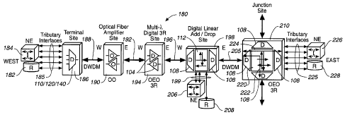
Reference is again made to Fig. 5 illustrating in a graphical representation
the decline of
optical transport pricing (costs) over a 100 km route. As seen by line 75, the
cost
effectiveness of the digital optical network in accordance with this invention
will take a
significant downward deviation due to, in a substantial manner, the reduction
of cost in the
manufacture of a TxP1C chip and a RxPIC chip that are completely in monolithic
chip form
which are all necessary components for signal light generation, signal
modulation and signal
combining and/or signal de-combining and detection provided as photonic
integrated circuits
(PICs) on a semiconductor-based chip, in particular a InP substrate based
chip. The TxPIC
and RxPIC may be formed on a single PIC chip or formed as separate PIC chips.
Thus, relative to forgoing, other features of this invention are the
replacement of analog
optical network sites, such as EDFA sites, with digital optical network sites
with optical
TxPIC and RxPIC chip modules of this invention. Reference in this connection
is made to
Figs. 6A-6D which is a simple view of the progression of what has happened
over the last
several years relative to optical transport systems or networks, which is, to
some extent, a
summary of the previous discussion relative to Figs. I and 2. Thus, as shown
in Fig. 6A,
optical transport networks initially started as a single signal which was
regenerated at OEO
REGEN sites 80 positioned at about 80 km distances along the optical span. The
network
architecture was a series of expensive OEO REGEN sites in the optical span.
Then came the
advent of WDM systems as shown in Fig. 6B and the inclusion of approximately
three to five
EDFAs 82 along the optical span, the distance between expensive OEO REGEN
sites 80
could be extended. This extension has grown further, as indicated in Fig. 6C,
with
approximately ten or more optical amplifiers 82 provided along the length of
the optical span
prior to OEO REGEN at 80. As previously indicated, the trend is to extend this
span distance
to even greater distances before any required signal regeneration as well as
developing
systems to do signal regeneration all or mostly all in the optical domain
toward eliminating
any extensive use of OEO REGENS. However, as taught in this invention, this
trend is not
necessary or even desirable since cost effective and competitive digital OEO
REGEN sites 84,
as shown in Fig. 6D, can be provided at least 10 times less than the cost of
OEO REGEN sites
80 previously deployed. In this way, the digital OEO REGEN sites 84 have come
full circle
relative to the advent of EDFA boosted WDM systems.
The architectural approaches of this invention provides for greater
flexibility, at both OEO
REGEN sites and 00 sites in upgrading them to provide added functionality
dependent on
local capacity requirements such as providing new or additional, 3R or 4R
fitnetionality, or
add/drops, switching, routing, grooming, thereby also reducing any backhauling
requirements.
23
CA 02463502 2010-09-13
Another feature of this invention is the elimination of some, if not all,
analog optic
components with the deployment of a digital optical network of this invention
including the
elimination for the need or requirement of dispersion compensation (DC)
compensators, PMD
compensators, gain flattening filters and equalizers, VOAs, optical switches
and OADMs,
broad range tunable semiconductor lasers, complex 000 REGENs and other band (S
or L
band) optical amplifiers. Such optical components are illustrated, in part, in
U.S. patent
application publication No. 20002/0044722A1 (OADM); U.S. patent 6,363,183B 1
(OADM);
U.S. patent 6,169,616B1 (OADM); U.S. patent 5,385,364B1 (optical switch); U.S.
patent
6,335,819131 ( 000 REGEN system); U.S. patent application publication No.
2001/0053008A1 (all-optical regeneration); U.S. patent application publication
No.
2002/0015201AI (network channel propagation extension with EDFAs deployed with
VOAs).
Another feature of this invention is the ease of added granularity in
wavelength or channel
scaling to provide for any incremental increase in channel capacity between
any two REGEN
sites through the modularity capability of the PICs brought about by this
invention,
Another feature of the architecture of this invention is the elimination of
the requirement
for expensive discrete, tunable DFB lasers and all-optical switching.
Another feature of this invention is the significant elimination in the number
of fiber
connections required in an optical transmitter, receiver or transponder so
that efficiency and
optical insertion loss can be greatly improved and fabrication labor and costs
can be greatly
reduced such as the time required and costs associated with alignment of
discrete active and
passive optical components as illustrated in connection. with Fig. 4.
A further advantage of the architecture of this invention is the elimination
of the
requirement, if desired, of on-chip or off-chip amplification via EDFAs which
are bandwidth
limited as well as SOAs in certain situations but, in any case, significantly
increase the power
budget of the PIC chip. Rather, the present invention permits usage of the
full bandwidth IR
range of optical fibers, such as, for example, from about 1250 nm to about
1650 nm through
the deployment of the digital OEO signal REGEN.
Another feature is that with the deployment of low-cost, digital OEO REGEN
sites of this
invention, the identification, isolation and location of faults in the network
becomes easier
since the span length between the REGENS can now be cost effectively smaller.
This
correlates with the fact that with the deployment of such digital OEO REGEN
sites, the
network will naturally have more locations where performance monitoring of the
channel
signals in the electrical domain is now possible.
24
CA 02463502 2010-09-13
Still further feature of this invention is the enhanced ability to easily
upgrade the capacity
of digital REGEN sites by simply adding additional RxPICs and TxPICs
interleaved with
existing RxPICs and TxPICs already deployed at the REGEN site to incrementally
add
channel capacity between any digital optical network REGEN sites.
A still another feature of this invention is a business model of providing a
digital optical
network deploying additional network capacity and functionality for future use
through the
semiconductor chip nature of including additional signal channels on TxPIC and
RxPIC chips
that may be deployed at a later time at the optical transport network
installation site.
Still a further feature of this invention is the provision of a digital
optical network that
eliminates the need for dispersion compensation (DC), PMD compensation, gain
flattening
filters and gain equalization, optical switches and OADMs, discrete tunable
laser sources, and
other high performance band analog amplifiers, such as L-band fiber
amplifiers.
Lastly, it is simple physics to understand that it is much more difficult to
"push around" or
handle photons as compared to electrons, such as in optical switching or cross-
connects. The
reason is that photons have higher momentum than electrons and, therefore,
take more energy
to handle them or take care of them. Therefore, it is always easier to deal
with electrons over
photons particularly relative to functions that a great deal of energy to
process propagating
light as in optical switching.
Therefore, according to the present invention there is provided:
a multiwavelength digital 3R optical channel signal generation (REGEN) site
(104),
comprising:
at least two semiconductor photonic integrated circuits (PICs), each
comprising an
optical receiver PIC chip (RxPIC) (140) and an optical transmitter PIC chip
(TxPIC) (120);
each of said TxPICs comprising, in integrated form on the chip, an array of
modulated
sources comprising a laser source and an electro-optic modulator (124, 126)
for providing
modulated channel signals, and an optical wavelength-selective combiner
comprising an
arrayed waveguide grating (AWG) (130) optically coupled to receive the
modulated signals
and provide a combined multiplexed channel signal on an output of the
respective TxPIC;
each of said RxPICs comprising, in integrated form on the chip, an optical
wavelength
selective decombiner comprising an arrayed waveguide grating (AWG) (144)
having an input
to receive a combined multiplexed channel signal and wavelength-selectively
demultiplex the
combined multiplexed channel signal into a plurality of channel signals, and a
plurality of
photodetectors (152(l) ... 152(12)) integrated with the wavelength selective
decombiner and
CA 02463502 2010-09-13
each optically coupled to receive one of the channel signals to convert the
same into a
wavelength selectively dernultiplexed electrical channel signal;
each of said at least two semiconductor photonic integrated circuits further
comprising
regeneration and cross-connect circuits (174) each coupled to one of said
TxPICs and one of
said RxPICs, respectively, wherein the wavelength-selectively decombined
channel signals
from each of the RxPICs having been received from an optical span, are
converted into
electrical channel signals, regenerated and at least some of the regenerated
electrical signals
are cross-connected to one of the TxPICs (120), converted into corresponding
optical signals
and multiplexed for transmission on another optical span.
It is another aspect of the invention to provide a digital optical network for
replacing at
least one optical amplifier site in an optical network optical span
comprising:
an optical-to-electrical (OE) receiver module formed on a single semiconductor
1nP
chip comprising an optical decombiner or demultiplexer to demultiplex a
multiplexed channel
signal received from the optical span comprising a plurality of optical
channel signals of
different wavelength approximately optimized to a standardized grid and a
plurality of
photodetectors for respectively receiving a demultiplexed channel signal and
produce
corresponding electrical channel signals;
an electronic linecard comprising electrical circuits to receive the
respective electrical
signals and perform 3R or 4R functions on the electrical signals; and
an electrical-to-optical (EO) transmitter module formed on a single
semiconductor InP
chip comprising a plurality of modulated sources to produce a plurality of
optical channel
signals; and an optical combiner or multiplexer that combines the optical
channel signals for
launching from the chip onto the optical span.
It is another aspect of the invention to provide a digital optical network for
a terminal
or OEO REGEN site, comprising:
a monolithic semiconductor lnP-based chip having at least one set of
information
signal transmitters comprising a plurality of modulated sources of different
operational
wavelengths approximately set and optimized to a standardized grid and an
optical combiner
or multiplexer that combines modulated optical signals from the modulated
sources into a
multiplexed information signal for launching and transport on an optical
medium, and at least
one set of information signal receivers comprising an optical decombiner or
demultiplexer that
demultiplexes a received multiplexed information signal received from the
optical medium
and a plurality of photodetectors to respectively receive a demultiplexed
signal from the
optical decombiner or demultiplexer for conversion into an electrical
information signal;
26
CA 02463502 2010-09-13
and electronic regenerator circuits to receive the electrical information
signals,
equalize and regenerate the electrical signals and provide the regenerated
signals to another
site or to another digital optical network.
It is another aspect of the invention to provide a digital optical network for
replacement of a terminal or OEO REGEN site utilizing discrete optical
components and
analog re-amplification sites operating in the optical domain, comprising:
a monolithic semiconductor IuP-based chip having at least one set of
information
signal transmitters and one set of information signal receivers respectively
comprising a
plurality of semiconductor lasers of different operational wavelengths set and
optimized to a
standardized grid, said lasers modulated to produce optical information
signals and a first
arrayed waveguide grating that combines the modulated signals into a
multiplexed
information signal for launching and transport on an optical medium, and
further comprising a
second arrayed waveguide grating that demultiplexes a received multiplexed
information
signal and a plurality of photodetectors to respectively receive a
demultiplexed signal for
conversion into an electrical information signal; and
electronic regenerator circuits to receive electrical information signals and
equalize or
regenerate the signals and provide the regenerated signals to another site or
to another digital
optical network.
It is another aspect of the invention to provide a long haul optical span
comprising:
a plurality of multiwavelength digital 3R regeneration (REGEN) sites spatially
positioned along the span;
each of said REGEN sites comprising at least two semiconductor photonic
integrated
circuit (PIC) chips each comprising an optical receiver PIC (Rx.PIC) and an
optical transmitter
PIC (TxPIC);
each of said TxPICs comprising, in integrated form on each chip, an array of
modulated sources for providing modulated channel signals, and an optical
combiner or
multiplexer optically coupled to receive the channel signals and provide a
combined
multiplexed channel signal on a chip output;
each of said RxPICs comprising, in integrated form on each chip, an optical
decombiner or multiplexer having an input to receive a combined multiplexed
channel signal
and demultiplex the multiplexed channel signal into a plurality of channel
signals, and a
plurality of photodetectors each optically coupled to receive one of the
channel signals convert
the same into an electrical signal;
27
CA 02463502 2010-09-13
said at least two semiconductor photonic integrated circuit chips coupled to
regeneration and cross-connect circuits where the demultiplexed electrical
channel signals
from one of the chips, having been received from the span are demultiplexed
and converted
into electrical signals, are regenerated and at least some of the regenerated
channel signals are
cross connected to the other chip and converted into optical signals and
multiplexed for
transmission on the optical span.
It is another aspect of the invention to provide a digital optical channel
signal
regenerator (REGEN) comprising:
at least two semiconductor photonic integrated circuits (PICs), one comprising
an
optical receiver PIC (RxPIC) and the other optical transmitter PIC (TxPIC);
said TxPIC comprising, in integrated form on each chip, an array of modulated
sources
for providing modulated channel signals, and an optical combiner or
multiplexer optically
coupled to receive the channel signals and provide a combined multiplexed
channel signal on
a chip output;
said RxPIC comprising, in integrated form on each chip, an optical decombiner
or
demultiplexer having an input to receive a combined multiplexed channel signal
and
demultiplex the multiplexed channel signal into a plurality of channel
signals, and a plurality
of photodetectors each optically coupled to receive one of the channel signals
to convert the
same into an electrical signal;
said at least two semiconductor photonic integrated circuits coupled to
regeneration
and cross-connect circuits where the demultiplexed electrical channel signals
from one of the
PICs, having been received from an optical span, are demultiplexed and
converted into
electrical signals, regenerated and at least some of the regenerated channel
signals are cross
connected to the other PIC and converted into optical signals and multiplexed
for transmission
on an optical span.
It is another aspect of the invention to provide a digital optical network
site
comprising:
at least one first short reach or long reach optical transmitter/receiver
module having at
least one transmitter and receiver photonic integrated chip;
integrated electronic processing circuits coupled to said first module to
receive from
and provide to electrical signals to said first module; and
at least one second long reach optical transmitter/receiver module having at
least one
transmitter and receiver photonic integrated chip, said integrated electronic
processing circuits
coupled to said second module to receive from and provide to electrical
signals to said second
module.
28
CA 02463502 2010-09-13
Other objects and attainments together with a fuller understanding of the
invention will
become apparent and appreciated by referring to the following description and
claims taken in
conjunction with the accompanying drawings,
BRIEF DESCRIPTION OF THE DRAWINGS
In the drawings wherein like reference symbols refer to like parts:
Fig. 1 is a schematic view of a first optical transport network as known in
the art.
Fig. 2 is a schematic view of a second optical transport network as known in
the art.
Figs. 3A-3E are graphic illustrations of the effects of nonlinearities and
other optical
impairments on a transmitted optical channel signal as is known in the art.
to Fig. 4 is a schematic view of the details of an optical Tx module and an
optical Rx module
deployed in the network shown in Fig. 2.
Fig. 5 is a graphic illustration of the variance in costs per signal channel
of various
deployed optical transport networks over time.
Figs. 6A-6D is a schematic illustration of the deployment of optical transport
networks
over approximately the last ten years and how, with the architecture disclosed
herein, the
network ends up looking like the original optical transport network but at
much reduced
manufacturing costs, much higher capacity, higher density equipment space, and
greater
optical integration.
Fig. 7 is a schematic illustration of the optical transport network of this
invention.
Fig. 8 is a schematic illustration of a 3R junction (switching) site utilizing
this invention.
Fig. 9 is a schematic illustration of a 3R AID site utilizing this invention.
Fig. 10 is a schematic illustration of a metro ring network utilizing this
invention.
Fig. II is a schematic illustration of a regional ring network utilizing this
invention,
Fig. 12 is a schematic illustration of a TxPIC chip utilized in the
architecture and practice
of the architecture of this invention.
Fig. 13 is a schematic layout of the TxPIC chip of Fig. 13.
Fig. 14 is a schematic illustration of a RxPIC chip utilized in the
architecture and practice
of the architecture of this invention.
Figs. 15A-15G are a series of illustrations showing different alternative
configurations for
the TxPIC and RxPIC utilized in the architecture and practice of this
invention.
Fig. 16 is a schematic illustration of a 3R OEO REGEN utilized in the
architecture and
practice of this invention.
Fig. 16A is a schematic illustration of digital 3R REGEN sites deployed along
an optical
span.
29
CA 02463502 2010-09-13
Fig. 17 is a schematic illustration of an OEO REGEN, capable of AID,
switch/route,
multiplexing and signal grooming utilized in the architecture and practice of
this invention.
Fig. 18 is a more detailed illustrative example of the features pertaining to
the architecture
of the digital optical network of this invention.
Fig. 19 is a schematic illustration of an alternative version of the optical
transport network
shown in Fig. 7.
Fig. 20 is another embodiment of architecture of the digital optical network
of this
invention utilizing multiple TxPIC and RxPIC chips.
Fig. 21 is a further embodiment of the digital optical network of this
invention at a
network terminal.
Fig. 22 is further embodiment of the digital optical network of this invention
at a network
OEO REGEN site.
DETAILED DESCRIPTION OF THE INVENTION
Reference is now made to Fig. 7 showing a digital optical network (DON) 100
comprising
this invention. Shown in Fig. 7 is a long haul fiber span with terminals 102
on either side of
the span and a plurality of digital WDM (OEO) 3R REGENs 104 provided along the
span.
REGENs 104 are shown in Fig. 16 and have optical transmitter and receiver PIC
chip
structures of the type shown in figs. 12-14 which are to be discussed later.
It should be
realized that other configurations, other than those illustrated in Fig. 12-
14, may be utilized in
the architecture of this invention, which other configurations are illustrated
in Fig. 15a-15G
herein as well as in the patent applications and patents referred to herein.
In this connection,
reference is also made to these patent applications and patents which discuss
in more detail,
the layout, fabrication and operation of TxPICs and RxPICs. In the
illustration of Fig. 16, the
RxPICITxPIC chips are back-to-back to provide for OEO functionality with
associated
electronic circuitry. As seen in Fig. 16, each digital REGEN 104 is
bidirectional and includes,
in each direction, i.e., is East and West, at least one RxPIC chip 140 and at
least one TxPIC
chip 120. The multiplexed optical information signals, propagating from West
to East or from
East to West, are received on optical link 139 or 141 and coupled into RxPIC
140 where they
are demultiplexed and converted into electrical signals. These converted
signals are taken off-
chip at lines 137 and are 3R processed at electronic circuit 172 and provided
to electrical cross
connect 174 where they are passed through or re-routed and passed through
cross connect 174
to electronic circuits 176 were they may be IR processed and provided
respectively to TxPIC
120 for conversion back into the optical domain and launched on fiber link 139
or 141. 3R
CA 02463502 2010-09-13
REGEN 104 is comparatively small relative current OEO systems since much of
the optical
circuitry is integrated on semiconductor type of chips.
It should be noted that TxPIC chip 120 and RxPIC chip 140 may be independently
deployed without the other in terminal sites, such as initial transmission of
optically
modulated signal channels from a source origin with TxPIC chip 120 or end
reception of
optically multiplexed signal channels at a receiver terminal with RxPIC 140.
Fig. 16A is an illustration of an optical span with a plurality of digital OEO
REGEN sites
104, one of which is shown in Fig. 7. Digital OEO REGENs 104 are deployed
along an
optical span at points where propagating channel signals minimally require I R
regeneration
but, instead, provide 3R regeneration. REGEN sites 104 can be deployed at
points where
optical fiber amplifiers, e.g., EDFAs, were previously deployed or are desired
to be deployed
to re-amplify the propagating channel signals, or can be deployed at digital
linear add/drop
sites and junction sites as depicted in Fig, 18, to be discussed later. As an
example, REGENS
104 are price-competitive with EDFA sites and, in addition, minimally provide
the capability
of signal re-amplification, re-shaping and retiming, the latter of which are
not capable of being
accomplished by an EDFA.
In addition to a pass-through OEO REGEN sites 104, the digital optical network
can also
be deployed as a 3R junction site 106 as illustrated in Fig. 8 or as a 3R A/D
site 114 as
illustrated in Fig. 9 to such existing sites or, more importantly, as an
upgrade to an existing
digital OEO REGEN site 104 to add switching or A/D functionality. In this
manner, DON is
modular in that it can be upgraded to include additional functionality
eliminating the need for
analog span engineering as is necessary in conventional optical analog systems
and sites. As
shown in Fig. 8, the junction site 106 includes a set of three OEO REGENs 108
with
appropriate line card circuits 110, each similar to the structure of REGEN 104
shown in Fig.
16, and a electrical cross connect 112 for electronically switching the OE
converted signals to
one of the three appropriate outputs through electronic matrix switching and
the signals are
EO converted via REGEN 108 and launched onto a fiber link.
In the A/D site 114 in Fig. 9, the OE converted signals at REGENs 108 may be
routed to a
different optical transport network or network element (NE) 118, which, for
example, may be
a switch or cross connect. The advantage of the DON architecture of this
invention is the
provision of a full flexible AID multiplexer replacing any optical fiber
amplifier site at a
competitive price with such amplifiers. Moreover, an already installed digital
3R OEO
REGEN site 104 can be conveniently upgraded to a digital AID site 1 14 to
provide any
configuration of selective channel add and drop.
31
CA 02463502 2010-09-13
Fig. 10 illustrates in simplistic form, a metro network comprising fiber ring
103 with
plural digital DON terminals 102. In a conventional metro network, these
terminals are
analog and engineered to provide for designed traffic requirements. If traffic
patterns change,
as indicated by dotted lines 105 where traffic demands have changed to direct
more channel
traffic to the East terminal 102, the East analog terminal must be redesigned
and changed to
meet the changing traffic needs and increase its capacity. Said another way,
such
conventional terminals with their discrete channel components are not forecast
tolerant.
Future traffic demand or changes in traffic patterns are not predictable. So,
to meet new or
changing traffic demands, the conventional site must be redesigned or re-
engineered
substantially from the beginning to include additional channels and additional
optical channel
add/drops to replace or bypass the existing site or node. Each such additional
add/drops
means additional dB insertion loss. This limits the capacity of network ring
103. Adding
additional EDFA sites to metro ring will help increase traffic capacity but
this is an expensive
approach. However, the deployment of digital terminal sites 102 in accordance
with the
architecture of this invention eliminates these problems by deploying digital
REGEN terminal
sites 102 on metro ring 103. In particular, the digital 3R REGEN sites 102
provide flexibility
in functionality choices modularity or scalability in increasing channel
service capacity
without requiring redesign engineering at the site. This is because the
modularity capability of
adding additional signal channels through the addition of TxPIC/RxPIC chips to
the system
board. Added functionality can be provided, such as, AID multiplexing,
switching, routing
and grooming through the added or replaced circuitry to include the additional
function at the
site directly to the existing digital 3R OEO REGEN site components. This
modularity
provides for a "pay as you go" system and eliminates the costly expense of
reengineering,
from the beginning, a conventional analog site to meet new capacity and/or
upgrade in
functionality. Also, in metro networks which include EDFA amplification sites
cannot be
upgraded without replacement of the existing analog OEO regeneration site. The
placement
of existing and future EDFA sites with digital REGEN sites of this invention
permits future
upgrade in functionality at those sites without later replacement of existing
equipment at the
site. This added modularity and upgrade capability is an important feature
provided by the
digital optical network of this invention.
Fig. I 1 is a simplistic form of a regional network which is principally the
same as the
metro network in Fig. 10 except has a larger distance and capacity ring 107
and the network
communication is more mesh-like in nature. As in the case of the metro network
of Fig. 10,
the regional network employing 3R OEO REGEN sites 102 provides more
flexibility in
32
CA 02463502 2010-09-13
system revamping or upgrading at comparatively much lower costs due to the
deployment of
transmitter and receiver photonic integrated circuit chips for channel signal
reception and
regeneration in the optical domain and 3R signal regeneration (re-amplifying,
reshaping and
retiming) via linecard chip set circuitry in the electrical domain. The
upgrade in channel
capacity is accomplished by adding additional PIC chip modules to increase the
capacity of
the network through an increase of the number of channels, such as illustrated
by multiple
TxPIC and RxPIC chips in the modules shown in Fig. 20, and upgrade in
functionality by
changing in circuitry such as an upgrade of a terminal site 102 in Fig. I1 to
an All) site 114
shown in Fig. 9.
Reference is now made to the details of one embodiment comprising TxPIC 120
and
RxPIC 140 which are respectively shown in Figs. 12 and 14, As previously
indicated, further
details concerning the architecture, structure, operation and functionality of
these PICs is set
forth in U.S. Patent Nos. 7,116,851; 7,283,694 and 7,079,715. With reference
first to Fig. 12,
TxPIC comprises an InP-based semiconductor chip which includes integrated
optical and
electro-optic components formed as a monolithic photonic integrated circuit.
Chip 120, in the
case here, comprises modulated sources of laser 124 and modulators 126.
Another type of
modulated sources is an array of direct modulated (DM) DFB or DFB lasers. Chip
120 has a
plurality of spatially aligned, integrated DFB lasers 124 each having a
different operating
wavelength approximated or optimized within a standardized wavelength grid,
such as the
ITU grid. Note that laser 124 may also be DBR lasers. There are twelve such
lasers and signal
channels in the embodiment shown in Fig. 12. However, there may be, for
example, any
number of such channels formed on the chip ranging, for example, from 4 to 40
channels
depending, for example, on their close spacing within acceptable cross-talk
limits. Some of
these channels may be redundant channels for use in place of inoperative
lasers or modulators
or EMLs. These DFB lasers 124 are wavelength stabilized as taught in the above
identified
provisional and patent applications. Each of the 12 channels in chip 120 also
includes an
optical modulator 126 to modulate the light output of a respective CW operated
DFB laser
124. Chip 120 may also include an optional optical array of PIN photodiodes
122 to monitor
the laser power and wavelength output of each DFB laser 124. Also, an optional
array of PIN
photodiodes 128, respectively following each modulator 126, may be utilized to
monitor the
power, chirp and extinction ratio of modulator 126. The modulator 126 may be
an electro-
absorption modulator or a Mach-Zehnder modulator. On the other hand, it should
be
understood that TxPIC 120 may not include modulators 126 and semiconductor
laser sources
124, albeit DFB lasers or D13R lasers, are directly modulated. As indicated
before, Figs. 12-
33
CA 02463502 2010-09-13
14 are merely illustrative embodiments for TxPIC and RxPIC chips, as other
configurations,
as noted in the Summary of Invention, may be utilized as well as illustrated
in the
configurations of Figs. 15A-15G.
Optical waveguides 129 are formed in the chip in a fan-out arrangement from
PINs 128 or
modulators 126 to the input slab 132 of an optical combiner 130, which is an
arrayed
waveguide grating (AWG) comprising input slab or free space region 132, a
plurality of
grating arms 134 and output slab or free space region 136 as known in the art.
AWG 130
combines the modulated signals on waveguides 129 in a multiplexed signal that
is provided on
one of the output waveguides 138 formed in chip 120 for taking the multiplexed
signal off-
chip and optical coupling to an aligned optical fiber. The waveguide 138
having the best
signal spectrum from AWG 130 is chosen as the output for launching onto a
coupling fiber,
such as coupling fiber 135 shown in Fig. 13.
Fig. 13 shows additional detail of TxPIC chip 120 of Fig. 12. It should be
noted that this
TxPIC chip 120 is just one embodiment of many that may be employed in a
digital optical
network. See, for example, the different embodiments illustrated in Canadian
patent
applications 2,463,278; 2,462,178; 2,463,500; 2,463,522; 2,602,975 and
Canadian patent no.
1,324,209. A particular example is the provision of integrated optical
amplifiers on a PIC
chip, such as SOAs or GC-SOAs.
To be noted is a twelve-channel chip of this size is fairly small comprising,
for example,
3.5 mm by 4.5 mm. The DFI3 laser sources are set on center-to-center spacing
of about 250
m. Also shown are the DC biasing for PINs 122(l)...122(12), DFB Laser 124(l)
... 124(12),
MODs 126(l)...126(12) and PINs 128(l)...128(12). On-chip heaters
125(1)...125(12),
which may strip heaters, for example, in proximity to each DFB laser, and are
independently
operated to maintain the peak operating wavelength of each laser to the
prescribed wavelength
of a standardized grid. Also, a heater 131 may be provided to control the
wavelength grid of
AWG 130 in conjunction with the control of the individual operating
wavelengths of DFB
lasers 124. This is explained in further detail in the above referenced
provisional applications
and their corresponding non-provisional applications. Lastly, each of the
modulators 126 has
a coaxial or coplanar electrode arrangement to provide to each MOD 126 an
electrically
modulated signal to each modulator 126(1)...126(12) for modulating the light
of the DFB
lasers 124, i.e., to accomplish EO signal conversion.
Reference is now made to Fig. 14 which shows the typical layout for a RxPIC
140. It
should be noted that this RxPIC chip 1.40 is just one embodiment of many that
may be
employed in a digital optical network. See, for example, the different
embodiments illustrated
34
CA 02463502 2010-09-13
in Canadian patent applications 2,463,278; 2,451,717 and 2,463,545. A
particular example is
the provision of integrated optical amplifiers on a PIC chip, such as SOAs or
GC-SOAs.
RxPIC 140 is an InP-based semiconductor chip that has an input at 145 to
receive a
multiplex optical signal from an optically coupled fiber link. An optical
amplifier 142 may be
integrated on the chip to boost the gain of the multiplexed signal prior to
demultiplexing.
Amplifier 142 may be a SOA or, more preferably, a gain-clamped SOA or optical
laser
amplifier. Such amplification can alternatively be done off-chip with an
optical fiber
amplifier at the input of waveguide 145. The multiplexed signal, In any case,
is received on
chip waveguide 147 and provided as an input to input slab or free space region
146 of AWG
144, AWG 144 comprises input slab 146, an array of grating arms 148 of
different lengths
and an output slab 150 as known in the art. Output slab 150 has a plurality of
outputs in the
first order Brillouin zone, one for each demultiplexed channel wavelength
signal, which are
respectively provided to PIN photodiodes 152(1)...152(12). Again, although
there are twelve
channels shown here for chip 140, there may be as many as 4 to 40 such channel
outputs from
AWG 14 with corresponding photodetectors. A higher Brillouin order output
channel 154
may also be provided on RxPIC chip 140 to provide a channel light output to
PIN photodiode
156 in order to monitor the wavelength, power of the signals or provide for
FEC capabilities.
The strategic impact in utilizing integrated optics in the form of the TxPIC
and RxPIC
chips 120 and 130 utilized in this invention is, by way of an example, is a
decrease in cost in
dollars per wavelength or channel by approximately 24 to I lower than a
comparable
conventional systems deploying discrete components as discussed earlier herein
and also price
competitive with conventional network, high performance analog EDFA sites.
Reference is now made to Fig. 15 which shows, in simplistic form, alternative
configurations for TxPIC chip 120 and RxPIC chip 140. Portions of these chips
can be
formed on separate chips. For example, as shown in Fig. 15A, the arrangement
shown in Fig.
12 is illustrated except without PIAIs 122 and 128. Chip 120A contains an
array of EMLs or
modulated sources 121 and chip 120B contains the optical combiner or AWG 130
and are
optically coupled together, such as by butt coupling. Moreover, other types of
optical
combiners can be utilized in any of these embodiments such as a MMI coupler or
an echelle
grating. This is the simplest form of TxPIC chip 120A with modulated sources
121
comprising DFB lasers 124 and EAMs 126. In the embodiment of Fig. 15 B, the
modulator of
choice for modulated sources 121 for chip 120A are MZMs 162, which are to
modulate the
CW output light received from DFB lasers 124. In the embodiment of Fig. 15C,
the
modulated sources comprise DFB lasers 12, provided on chip 120A, and are
direct modulated
CA 02463502 2010-09-13
(DM) lasers which are known in, the art. Their outputs are optically coupled
to optical
combiner 130 on chip 120B. This is the simplest form of a TxPIC chip 120
comprises an
array of DFI3 lasers 124 and an optical combiner 130.
Fig. 15D illustrates the simplest form of a RxPIC chip 140 comprising an
optical
decombiner 144 on chip 140A and an array of photodetectors 152 formed on chip
140B which
may be an array of PIN photodiodes or avalanche photodiodes. Again, chips 140A
and 140B
may be formed as a single monolithic chip 140 or chip 140B may be optically
coupled, such
as by butt-coupling, to chip 1408.
In The embodiment of Fig. 15E, separate EML or modulated source chips 120A,
and
120A2 are provided each with arrays of DFB lasers 124 and modulators 126. Each
chip 120A,
and 120A2 may be optically coupled, such as via optical butt coupling, to
optical combiner
130 formed on chip 1208. In the embodiment of Fig. 15F, optical combiner 144
on chip
140A may have its outputs optically butt coupled to two different photodiode
chips 140B1 and
140B2 each having separate arrays of photodiodes 152 for detection of channel
signals.
In the embodiment of Fig. 15G, a bidirectional OE REGEN 170 can be formed with
four
semiconductor chips 120A, 1208, 140A and 140B optical coupled as shown.
Alternatively,
chips 120A, 1208, 140A and 140B may be form on a single monolithic
semiconductor chip
170 or as separate PIC chips 120 and 140 as illustrated in Figs. 15A and 15D.
Reference is now made to Fig. 17 which illustrates another OEO REGEN
configuration
176 of this invention. In this configuration, multiplexed signal channels are
received from
optical line 139, as an example, by TxPIC/RxPIC chip 140A, demultiplexed and
OE
converted for signal regeneration and cross-switching at digital regeneration
circuits 178. The
functions performed on the demultiplexed electrical signals may include 3R,
A/D
multiplexing, switch or route, multiplexing, such as TDM multiplexing,
wavelength
conversion or signal grooming as all known in the art. Re-routed signals from
TxPIC/RxPIC
module 104A may be switched off for transmission on optical lines 177 or 179
from
regeneration circuits 178 and EO converted at TxPIC/RxPIC modules 173 and 179,
respectively, multiplexed and launched on one or more optical lines 177 and
179. On the
other hand, the rejuvenated channel signals may be switched to TxPIC/RxPIC
chip(s) 120 and
launched on optical line 140. Conversely, channel signals received from
optical lines 177 and
179 are demultiplexed and OE converted at TxPIC/RxPIC modules 177 and 179 and
regenerated and rerouted by regeneration/cross-switching circuits 178 to
either or both of
TxPIC/RxPIC modules 104A and 104E for launching on optical lines 139 and 141,
respectively.
36
CA 02463502 2010-09-13
Fig. 18 illustrates various system components shown in Figs. 7-9, 16 and 17 in
a digitally
amplified wavelength network (DAWN) 180 which is one of the main focuses of
this
invention. On the West side of DAWN 180 is terminal node or site 186 which
includes
TxPIC and RxPIC chips 120 and 140 and electronic linecards 110 for sending and
receiving
channel signals relative to optical link 188 and to provide channel signals to
tributary
interfaces 185 between client devices such as a network element (NE) 184, for
example, a
switching device, and a routing device 182. The fiber link 188 connects
terminal site 186 to
an optical fiber amplifier site 190. Site 190 is a standard optical fiber
amplifier site for
amplifying WDM channel signals propagating bidirectionally in the optical
transport network.
Site 190 is a high performance amplifier site that performs 2R, i.e., both
optically re-
amplification and reshaping of the channel signals in either direction on the
network. Also,
optical dispersion compensation may be performed at this site, e.g., deploying
DCF. The fiber
link 192 connects the optical amplifier site 190 to a digital 3R site 194
deploying OEO
functionality. Site 194 is the same type of site, as site 104 in Fig. 7 or the
detailed structure
shown in Fig. 16. Digital amplifier site 194, therefore, performs electronic
signal
regeneration, (re-amplification, reshaping and retiming). The fiber link 196
connects digital
3R site 194 to a digital linear A/D site 198. This site 198 is the same type
of site as site 114 in
Fig. 9. As indicated by the arrows in this site, a portion of the channel
signals are added from
or dropped to local tributary interfaces 199 to local devices such as network
element (NE) 206
and router 208. The fiber link 205 connects digital linear AID site 198 to
junction node or site
210 located at the junction of multiple transmission fibers from different
directions, i.e., from
East, West, North and South. This site is the same type of site as site 106 in
Fig. 8. The
channel signals are groomed individually, or in groups, and then may be
generally switched to
other optical fiber links, such as indicated by arrow 222, or pass through to
tributary interfaces
225 to client devices such as network element (NE) 226 and router 228 and also
switched to
other optical fiber links as indicated by arrow 224. The other arrows indicate
other possible
cross-connect paths of channel signals at junction site 210.
In all of the foregoing sites, except, of course, the optical fiber amplifier
site 190, the
digital DWDM components with the RxPIC and TxPIC chip components 120 and 140,
such as
shown in Figs 12 and 14, which are at the front end of the architecture
fabric, are key to the
digital architecture not only in terms cost competitiveness but also in terms
of providing
modularity to the architecture for easy and low cost upgrade of channel
capacity.
It should noted that with respect to performance monitoring, the digital
optical network of
this invention provides for a first time increased accessibility to more
points along an optical
37
CA 02463502 2010-09-13
transport network than previously before in providing the ability to verify
the BER on any
channel at any point on the span where a low cost DON system is installed. DON
provides
not only immediate access to the network for upgrading but also provides
closer point-to point
ability to localize and isolate network errors, particularly error rates. As
can be readily
understood with reference to Figs. 6C and 6D again, that DON affords now a low
cost
replacement of the amplifier sites 82 in Fig. 6C with digital network sites
that provide
immediate access to the network which can isolate errors between points of DON
installations
as is illustrated in Fig. 6D. As can be seen form Fig. 6C, there would be many
more point
along a long haul system to monitor and investigate a point providing
particular problems with
respect to transmission faults or errors. Thus, a main point then is that the
digital optical
network of this invention has many more points where the electrical signal and
hence the bit
error rate is accessible, so that the ability to troubleshoot span and
equipment problems is
greatly enhanced. Long haul systems maintain the signal in the optical domain
for 600 km to
3200 km and hence pinpointing any degradation in signal quality is extremely
difficult and
has been a severe limitation in gaining acceptable of long haul optical
systems. The ability to
verify the error rate on any channel at the end of every fiber link or span or
even every few
spans or links or at previously installed optical amplifier sites is a
tremendous advantage in
network management to immediately isolate and locate points of system errors
and other
network faults through shorter distal links along the entire network.
Reference is now made to Fig. 19 which is a modification of the long haul span
shown in
Fig. 7. Fig. 19 is the same as Fig. 7 except, in addition, low cost EDFAs 230
are placed along
the fiber links in the optical span between terminals 102. Since OEO REGENs
104 are
deployed in lieu of conventional, discrete component OEO sets and EDFA sites,
the boost in
gain provided by low cost EDFAs 230 may be provided by low performance fiber
amplifiers,
i.e., amplifiers that have relaxed optical characteristics or parameters such
as spectrum gain
flattening, gain tilt, OSNR performance or noise figure, and there is no
problematic
characteristic of concatenated line amplifier gain spectrum reduction, gain-
tilt or gain ripple
accommodation. The deployment of low performance, low cost EDFAs permits a
"skip one"
or higher topography to be accomplished at the expense of a low performance
EDFA because
the channel signals will be, soon thereafter, 3R regenerated in any case.
"Skip one" is a
network approach of skipping the placement of one digital OEO REGEN an
replacing it with
an optical amplifier which may already exist or is newly inserted.
Reference is now made to Fig. 20 and digital optical network 240. Network 240,
for
simplicity, is illustrated as a unidirectional optical communication link,
although the network
38
CA 02463502 2010-09-13
could be bidirectional with the addition of RxPICs 246 in Tx module 242 and
TxPICs in Rx
module 244, such as illustrated in Figs. 16 and 17. Fig. 20 illustrates an
optical transport
network comprising a Tx module 242 having a plurality of TxPIC chips 246
comprising
TxPICs 1 through 8, which each can have 4 to 40 channels per PIC. EO signal
conversion
occurs in each TxPIC 246 through direct modulation of the respective DFB
lasers or through
modulation of on-chip optical modulators. The multiplexed channel wavelength
band outputs
from the respective TxPIC chips 246 are passed onto waveguides 247 to
wavelength band
multiplexer 248 for multiplexing all the channel bands from TxPIC chips 246
into a final
multiplexed or WDM channel signal for transport on fiber link 252. In a
bidirectional digital
optical network, device 248 is a band MUX/DEMUX module (BMDM) to multiplex or
demultiplex channel bands to and from optical link 252 as known in the art.
The multiplexed
signals may, then, number from 32 to 320 channels and are boosted in signal
gain by post-
optical amplifier 250 and launched on fiber link 252.
The multiplexed multi-band signal is then received at RxPIC Module 244 where
the
multiplexed signal may be initially amplified by pre-optical amplifier 254
and, thereafter,
band demultiplexed or de-interleaved or both at 256 into multiplexed channel
bands and the
bands are then passed via optical waveguides 257 onto the individual
respective RxPIC chips
258 comprising RxPICs 1-8, where they are demultiplexed into their individual
channel
signals for OE conversion for off-chip transfer to electronic processing
circuitry. It can be
seen that Tx and Rx modules 242 and 244 are compact with the deployment of
plural
semiconductor PIC chips 246 and 258 in modules 242 and 244.
Reference is now made to Figs. 21 and 22. Another embodiment of a digital
optical
network (DON) is one that utilizes: (I) low-cost PIC transmit and/or receive
module(s) for the
transmission interfaces in the system either at terminals or OEO REGENs, (ii)
a highly
integrated signal processing chip or chip set, and (iii) low-cost PIC transmit
and/or receive
module(s) for tributary interfaces to customer clients. A schematic of an
embodiment of a
DON terminal 300 is shown in Fig. 21 and for a DON OEO REGEN site 320 is shown
in Fig.
22. It should be recognized that the embodiment in Fig. 21 is similar to the
digital optical
network 180 shown in Fig. 18 at terminal site 186. In the embodiment in Fig.
21, PIC
modules are utilized to provide very low cost OE or EO conversion on both the
transmission
side of the terminal 300, often referred to now as long-reach (LR), and the
tributary side of the
terminal 300, often referred to as short-reach (SR). The tributary SR-PIC
module(s) 306 in
Fig: 21 is an optical module that has either combined transmit and receive
functions
(transceiver) or separate transmitter or receive modules of the type
previously explain herein,
39
CA 02463502 2010-09-13
Each tributary transmit module is characterized by having multiple distinct
electrical signal
inputs 308 and multiple distinct optical fiber signal outputs 310 which are
routed to multiple
physical locations of a client or clients. Similarly, each tributary receiver
module is
characterized by having multiple distinct optical fiber signal inputs 312 from
different
locations and multiple electrical signal outputs 314. For a PIC tributary
transceiver, these are
combined in one module. Also, note that a transmitter, receiver, or
transceiver 306 in Fig. 21
may also be replaced with multiple transmitters, receivers, or transceivers
that each may have
multiple channels per module. The tributary modules are then interfaced to
integrated
electronic processing circuits 304 which are then interfaced to the
transmission LR-PIC
modules 302 via electrical signal inputs 316 and optical signal outputs 318.
The integrated
electronic processing circuits 304 comprises either a single IC chip in the
most preferred
embodiment or a IC chip set, that contain, in either case, more than one of
the following
functions on a given chip; clock and data recovery (CDR), serializing and
deserializing
(SERDES), forward error correction (FEC), crosspoint switching, and electronic
signal
compensation, i.e., equalization of frequency dependent attenuation of the
electrical signal
pulse or skew or GVD of the optical signal pulse, framing, and associated
switching fabric.
Furthermore, it is preferred that the single IC chip embodiment include all of
the above
identified functions for all signal channels on a single chip. Alternatively,
multiple chips may
be utilized to cover either multiple channels and/or multiple groups of
functions. This DON
terminal 300 is described as an ultimate terminal architecture in that it has
a minimum number
of optical-electronic and electronic components and hence has advantages of
low cost with
accompanying higher density. The minimum cost is realized by virtue of the
minimum
number of such components which reduces the total component cost, Furthermore,
the
manufacturing cost is reduced since the number of components is reduced,
reducing the
complexity of the manufacturing process. The improved density of such a system
has several
advantages. First, the footprint of the system is dramatically reduced with
less components,
which reduces the overall space requirements for carrier providers.
Furthermore, the increase
in density means that an increased number of optical and electrical components
can be
implemented on a given system board in a carrier provider's rack. The ability
to implement
an increased number of functions of the components on a single board for a
group of signal
channels is extremely advantageous in that it eliminates or otherwise greatly
reduces the
backplane complexity of the telecom system. Sending high-speed signals across
the
backplane of a telecom system results in significantly increased cost and
complexity, In the
ultimate case, the tributary interfaces, electronic processing, and
transmission interface
CA 02463502 2010-09-13
functions are captured on a single PC board. The ability to accomplish this
task is enabled by
having high-density components LR-PIC and SR-PIC chip modules. Without the
improved
density of these modules, the integrated electronic processing chip(s) are of
significantly
diminished value or may not even be feasible in a telecom system. The density
of the PIC
chips translates into the decreased distance that high-speed signals must be
routed on a PC
board before they reach the integrated electronic processing chip(s). Without
PIC chips,
signals at the line rate of the system must be routed over significant
distances on the board,
resulting in substantial degradation of the transported signals and increased
cost and
complexity of the board itself. Thus, the PIC modules enable the utilization
of low cost
integrated electronic processing chips in a digital optical network.
The foregoing also applies to a DON OEO REGEN site which is shown in Fig. 21.
The
0130 regen site 320 is similar to terminal 300 with the exception that the
tributary SR-PIC
modules 306 are replaced with transmission LR-PIC modules 322. All of the
advantages
stated above for DON terminal 300 similarly apply to DON OEO REGEN site 320.
In Fig.
22, West to East bound traffic, a.i...).N, is received by LR-PIC modules(s)
322 which provides
electrical signal outputs 326 to integrated electronic processing circuits
328. Circuits 328
provide an electrical signal output 332 to another or other LR-PIC module(s)
322 to provide
optical signal outputs, 7,,...IN, for East bound traffic. By the same token,
East to West bound
traffic, Xj.JM, is received by LR-PIC modules(s) 322 which provides electrical
signal outputs
330 to integrated electronic processing circuits 328. Circuits 328 provide an
electrical signal
output 324 to another or other LR-PTC module(s) 322 to provide optical signal
outputs,
Xj...?,M, for West bound traffic.
While the invention has been described in conjunction with several specific
embodiments,
it is evident to those skilled in the art that many further alternatives,
modifications and
variations will be apparent in light of the foregoing description. Thus, the
invention described
herein is intended to embrace all such alternatives, modifications,
applications and variations
as may fall within the spirit and scope of the appended claims.
41