Note: Descriptions are shown in the official language in which they were submitted.
CA 02463545 2004-04-08
WO 03/102659 PCT/US02/32110
AN OPTICAL SIGNAL RECEIVER PHOTONIC INTEGRATED CIRCUIT (RxPIC),
AN ASSOCIATED OPTICAL SIGNAL TRANSMITTER PHOTONIC INTEGRATED
CIRCUIT (TxPIC) AND AN OPTICAL TRANSPORT NETWORK UTILIZING
THESE CIRCUITS
BACKGROUND OF THE INVENTION
Field of the Invention
This invention relates generally to optical telecommunications and more
particularly to the
deployment of photonic integrated circuits (PICs), in particular, optical
receiver photonic
integrated circuits (RxPICs) and transmitter photonic integrated circuits
(TxPICs) utilized in
optical transport networks.
Description of the Related Art
The employment of photonic integrated circuits (PICs), also sometimes referred
to as
planar lightwave circuits (PLCs), are on the rise in optical telecommunication
systems. These
devices provide the integration of both active and passive optical components
on a single
substrate and are integrated with other optical components to form a multi-
functional optical
device for use in such systems. The gravitation to PICs is strong because it
leads to utility of
providing an entire system function, let alone a component function, in a
single chip in a
single package. Compared to the deployment of discrete optical components,
such monolithic
PIC chips can significantly reduce the size of optical components necessary in
the optical
system, albeit an optical transmitter (TxPIC) or optical receiver (RxPIC), for
example, as well
as significantly reduce the over cost of the system
Optical PICs are already known in the art. As related to an optical receiver
on a chip, the
article to M. Zirngibl et al. entitled, "WDM receiver by Monolithic
Integration of an Optical
Preamplifier, Waveguide Grating router and Photodiode Array", ELECTRONIC
LETTERS,
Vol. 31(7), pp. 581-582, March 30, 1995, discloses a 1 cm by 4 mm PIC chip,
fabricated in
InP, that includes the integrated components comprising an optical amplifier
(SOA) optically
coupled to an AWG DEMUX having a plurality of different signal channel outputs
each
coupled to a respective photodiode (PD) in an array of on-chip photodiodes.
The SOA boosts
the multiplexed input channel signals. The AWG DEMUX demultiplexes the signals
into
separate channel signals which signals are respectively detected by the array
of PDs. The
optical receiver chip may also be placed on a thermoelectric cooler (TEC) so
that the spectral
response or wavelength grid of the AWG can be fine tuned. A similar PIC chip
configuration
is shown in U.S. patent 5,913,000 to Doerr et al. but relates to a laser
structure without an
array of photodiodes, but rather an array of second optical amplifiers in
their place, and where
the PIC chip facets include reflective mirror surfaces to form multiple laser
cavities. Further,
an article to C. Cremer et al. entitled, "Grating Spectrograph Integrated with
Photodiode Array
CA 02463545 2004-04-08
WO 03/102659 PCT/US02/32110
in InGaAsP/InGaAs/InP", IEEE Photonics Technology Letters, Vol. 4(1), pp.
108110, January
1992, discloses a 4 mm by 7 mm InGaAsP/InP chip comprising a grating
demultiplexer
integrated with a photodiode array. The grating demultiplexer comprises a slab
waveguide
having multiple input waveguides and output waveguides to and from the slab.
The slab has
one end as a reflective mirror and, thus, "mirrors" one half of a full slab
waveguide structure.
The output waveguides from the slab are respectively coupled to an array of
photodiodes
integrated on the InP chip. See also the papers of J. B. Soole et al.,
Integrated Grating
demultiplexer and PIN array for High Density Wavelength Division Multiplexed
Detection at
1.5 mm", ELECTRONIC LETTERS, Vol. 29, pp. 558-560, 1993; M. R. Amersfoort et
al.,
"Low-Loss Phased-Array Based 4-Channel Wavelength Demultiplexer Integrated
with
Photodetectors", IEEE Photonics Technology Letters, Vol. 6(1), pp. 62-64,
January 1994; and
S. Chandrasekhar et al., "Monolithic Eight-Wavelength Demultiplexed Receiver
for Dense
WDM Applications", IEEE Photonics Technology Letters, Vol. 7(11), pp. 1342-
1344,
November 1995.
A combination WDM/PD array is shown in the article of F. Tong et al. entitled,
"Characterization of a 16-Channel Optical/Electronic Selector for Fast Packet-
Switched
WDMA Networks", IEEE Photonics Technology Letters, Vol. 6(8), pp. 971-974,
August
1994, except that, in the case here, the InGaAs/GaAs PDs are on a separate
chip integrated
with electronic transimpedance amplifiers, selectable switches and output
limiting amplifier.
Light generated from the multiple output waveguides of a separate AWG DEMUX
chip is
focused through a lens array to the array of photodetectors or photodiodes
(PDs).
See also the article of B. Glance et al. entitled, "Applications of the
Integrated Waveguide
Grating Router", Journal of Lightwave Technology, Vol. 12(6), pp. 957-962,
June 1994,
which shows multiple applications for AWG devices with multiple inputs/outputs
and their
integration with various types of active components.
In some of the foregoing disclosures, optical semiconductor amplifiers (SOAs)
are
employed to boost the incoming channel signals such as from an optical link.
Thus, the first
on-chip optical component is an active component comprising an SOA to amplify
the channel
signals. Since these signals are of different wavelengths, however, the gain
of the SOA is not
equally distributed to all of the channel signals and, as a result, the
signals to be amplified do
not receive the same gain. This is a problem because the signals should have
substantially
equal intensity or power before they are demultiplexed; otherwise, some of the
channel signals
will have significantly degraded BER due to the dynamic range of the receiver
photodiodes
and transimpedance amplifiers.
OBJECTS OF THE INVENTION
It is an object of this invention to provide, in combination, photonic
integrated circuit
(PIC) chips in combination with electronic circuit chips useful in optical
transport networks,
-2-
CA 02463545 2004-04-08
WO 03/102659 PCT/US02/32110
in particular digital optical networks disclosed in U.S. patent application,
Serial No. (P016),
filed October 8, 2002, which is incorporated herein by reference.
It is another object of this invention to provide an optical receiver photonic
integrated
circuit (RxPIC) with improved performance.
It is a further object of this invention to provide an optical transport
network utilizing an
optical receiver photonic integrated circuit (RxPIC) and or optical
transmitter photonic
integrated circuit (TxPIC) or a transceiver or transponder in an optical
transport network.
It is another object of this invention to RxPIC monolithic chip that comprises
at least one
gain clamped optical semiconductor amplifier (GC-SOA), an optical
demultiplexer, preferably
an AWG DEMUX, and an .array of photodiodes (PDs), preferably an array of PIN
PDs, all
integrated on one monolithic PIC chip.
It is further object of this invention to provide an RxPIC chip that provides
redundancy to
improve chip yield.
SUMMARY OF THE INVENTION
According to this invention, a optical receiver photonic integrated circuit
(RxPIC)
comprises a single chip casted from an InP wafer and is made from Group III-V
elemental
materials in the InGaAsP/InP regime with fabrication accomplished through
selective
metalorganic vapor phase epitaxy (MOVPE) or also known as metalorganic
chemical vapor
deposition (MOCVD). Integrated on the chip, starting at the input end which is
coupled to
receive multiplexed optical data signals, may include an on-chip input optical
amplifier, an
optical demultiplexer (DEMUX), and a plurality of on photodiodes (PDs) each to
receive a
respective demultiplexed data signal from the DEMUX for optical-to-electrical
signal
conversion. The RxPIC chip input is optically coupled to receive a multiplexed
channel
signals from an optical transport network and are optically coupled to a
signal demultiplexer
providing a plurality of channel signal outputs optically coupled to an array
of photodiodes,
such as PIN photodiodes (PDs) or avalanche photodiodes (APD5). The PDs each
have a
contact pad for transfer of the generated electrical signal off the chip or,
alternatively, the
RxPIC can include on-chip integrated transimpedance amplifiers to receive
electrically
converted channel signals.
A RxPIC chip may provide for minimal optical loss between the input optical
fiber from
the optical transport network optical fiber link and a first point of
amplification in order to
achieve high optical signal to noise ratio (OSNR). This can be accomplished by
having an
optical amplifier at the chip input such as, for example, on-chip, gain-
clamped semiconductor
optical amplifier or a GC-SOA or an off-chip EDFA or Raman amplifier. If no
amplification
is to be provided at the input of the RxPIC chip, then the channel signal
demultiplexer will
have to provide minimal insertion loss. In this case, the preferred optical
demultiplexer is an
-3-
CA 02463545 2004-04-08
WO 03/102659 PCT/US02/32110
AWG so that if it is properly designed, it will provide minimum loss as
compared to other
types of optical demultiplexers, also which are disclosed herein, as well as
also provide for a
filter function to select one optical channel from the plurality of channels
with minimal optical
crosstalk and to eliminate undesired noise carried along with the channel
signals, such as ASE
and the gain clamping lasing signal.
One important feature disclosed is the employment of an on-chip, gain clamped
semiconductor optical amplifier (GC-SOA) rather than a semiconductor optical
amplifier
(SOA). The use of a GC-SOA provides for a saturated SOA that has continuous
gain in spite
of continuous changes in the incoming optical multiplexed channel signal gain;
otherwise,
without the gain clamped signal of the GC-SOA, the gain provided by the SOA
would gain-
starve higher signal wavelengths over time. For purposes of enhancing the
yield of optical
receiver photonic integrated circuit (RxPIC) chips produced from an InP wafer,
a plurality of
GC-SOAs are utilized at the input of the RxPIC chip and tested to see which
one best matches
the optical mode from the GC-SOA to the AWG to ensure polarization
insensitivity with low
loss and minimal back reflections from the AWG.
It is another feature of this invention to place integrated SOAs in an RxPIC
chip between
the demultiplexer and the array of photodiodes, with one in each waveguide
from a
demultiplexer output to a respective photodiode. The SOAs optimize the
received
demultiplexed channel signals by render them all of equalized intensity or
power so that the
responsivity of the photodiodes will all be substantially the same.
Other objects and attainments together with a fuller understanding of the
invention will
become apparent and appreciated by referring to the following description and
claims taken in
conjunction with the accompanying drawings.
BRIEF DESCRIPTION OF THE DRAWINGS
In the drawings, the same reference symbols also refer to the same parts
illustrated in other
drawings.
Fig. 1 is a schematic diagram of an optical receiver photonic integrated
circuit (RxPIC)
chip comprising this invention.
Fig. 2 is a schematic diagram of another embodiment of a RxPIC chip comprising
this
invention.
Fig. 3 is a detailed schematic diagram of a gain clamped-semiconductor optical
amplifier
(GC-SOA) and DEMUX of a RxPIC chip comprising this invention where multiple GC-
SOAs
are provided which also include an integrated heater for each GC-SOA.
Fig. 4 is a schematic diagram of an RxPIC chip illustrating a further
embodiment
comprising this invention.
-4-
CA 02463545 2004-04-08
WO 03/102659 PCT/US02/32110
Fig. 5 is a more detailed schematic diagram of the RxPIC chip of Fig. 4
comprising this
invention and illustrating the optical demultiplexer as an arrayed waveguide
grating
demultiplexer (AWG DEMUR) in the layout of the optical components in the RxPIC
chip.
Fig. 5A is a detailed schematic view diagram of the GC-SOA/AWG vernier input
which is
a feature of this invention.
Fig.6 is a schematic diagram of an alternative embodiment of the detailed
RxPIC chip
layout of Fig. 5 comprising this invention.
Fig. 7 is a schematic diagram of a GC-SOA with greater detail of mode adaptors
(MAs) at
its input and output.
Fig. 7A is a schematic diagram of a GC-SOA in an RxPIC chip that includes an
input
waveguide to the GC-SOA at an angle relative to the chip input facet to
suppress spurious
inputs to the GC-SOA other than the incoming channel signals.
Fig. 7B is a schematic diagram of a plan view of a GC-SOA in a RxPIC chip
where the
chip includes a curved-shaped GC-SOA with its front end at an angle relative
to the chip input
facet to suppress spurious inputs to the GC-SOA other than the incoming
channel signals.
Fig. 8A is a schematic cross sectional diagram of a specific embodiment of a
GC-SOA
that may be utilized in the RxPIC of this invention, illustrating an example
of the
semiconductor layers of the device.
Fig. 8B is a schematic cross sectional diagram of a specific embodiment of a
PIN
photodiode that may be utilized in the RxPIC of this invention, illustrating
an example of the
semiconductor layers of the device.
Fig. 8C is a schematic cross sectional diagram of a specific embodiment of an
AWG that
may be utilized in the RxPIC of this invention, illustrating an example of the
semiconductor
layers of the device.
Fig. 9 is a plan view of a GC-SOA that may be utilized in this invention
illustrating a
segmented electrode contact for applying a bias to the device.
Fig. 10 is a plan view of another view of a GC-SOA that may be that may be
utilized in
this invention illustrating a tapered electrode contact for applying a bias to
the device.
Fig. 11 is schematic cross-sectional diagram of an embodiment of a GC-SOA that
may be
utilized in this invention illustrating an example of the semiconductor layers
of the device
with a longitudinal monotonically increasing GC-SOA current channel from the
forward end
to the rearward end of the device.
Fig. 12 is a schematic cross sectional diagram of a first type of GC-SOA that
may be
utilized in this invention, to wit, a DFB type GC-SOA.
-5-
CA 02463545 2004-04-08
WO 03/102659 PCT/US02/32110
Fig. 13 is a schematic cross sectional diagram of a second type of GC-SOA that
may be
utilized in this invention, to wit, a DBR type GC-SOA.
Fig. 14 is a schematic side view diagram of a third type of GC-SOA that may be
utilized in
this invention, to wit, an external injection type GC-SOA.
Fig. 15 is a schematic cross sectional diagram of a fourth type of GC-SOA that
may be
utilized in this invention, to wit, a VCSEL type GC-SOA.
Fig. 16 is the first of several figures following this figure schematically
illustrating a first
embodiment for eliminating ASE generated by the GC-SOA from a RxPIC chip.
Fig. 16A is a second embodiment illustrating another approach for eliminating
ASE
generated by the GC-SOA from the RxPIC chip.
Fig. 17 is a third embodiment for eliminating ASE generated by the GC-SOA from
the
RxPIC chip.
Fig. 18 is a fourth embodiment for eliminating ASE generated by the GC-SOA
from the
RxPIC chip.
Fig. 19 is a fifth embodiment for eliminating ASE generated by the GC-SOA from
the
RxPIC chip.
Fig. 20 is a sixth embodiment for eliminating ASE generated by the GC-SOA from
the
RxPIC chip.
Fig. 21 is a seventh embodiment for eliminating ASE generated by the GC-SOA
from the
RxPIC chip.
Fig. 22 is an eighth embodiment for eliminating ASE generated by the GC-SOA
from the
RxPIC chip.
Fig. 23 is a schematic plan view of an AWG DEMUR having means to provide
polarization mode selectivity that may be utilized in this invention.
Fig. 24 is a schematic plan view of an AWG DEMUX having second optical
amplifier
means in the form of an array of optical semiconductor amplifiers (SOAs) in
the arrayed arms
of the AWG DEMUX that may be utilized in this invention.
Fig. 25 is a schematic side view of a type of photodetector for employment
with this
invention, to wit, a PIN photodiode (PD) as known in the art.
Fig. 26 is a schematic side view of another type of a photodetector for
employment with
this invention, to wit, an avalanche photodiode (APD) as known in the art.
Fig. 27 is a schematic side view of further type of a photodetector for
employment with
this invention, to wit, an interdigitated contact or MSM photodetector as
known in the art.
-6-
CA 02463545 2004-04-08
WO 03/102659 PCT/US02/32110
Fig. 28 is a schematic side view of a first embodiment of a flip-chip bonded
RF submount
board with an RxPIC chip comprising this invention.
Fig. 28A is a schematic side view in exploded form of a second embodiment of a
flip-chip
bonded RF submount board with an RxPIC chip comprising this invention.
Fig. 28B is a schematic side view in exploded view of a third embodiment of a
flip-chip
bonded RF submount board with an RxPIC chip comprising this invention.
Fig. 29 is perspective schematic illustration of a wire bonded RF submount
board with an
RxPIC chip comprising this invention.
Fig. 30 is a schematic plan view of architecture for coupling staggered output
PD pads
formed on the RxPIC which pads are wire bonded to corresponding input pads on
multiple RF
submount boards to control coupling impedance.
Fig. 31 is a schematic side view of one integrated approach for forming a mode
adapter
(MA) at the input of a GC-SOA on the RxPIC chip.
Fig. 32 is a schematic plan view of another integrated approach for forming a
mode
adapter (MA) at the input of a GC-SOA on the RxPIC chip.
Fig. 33 is a schematic view of a first embodiment for eliminating the residual
clamping
signal emanating from the GC-SOA.
Fig. 34 is a schematic view of a second embodiment for eliminating the
residual clamping
signal emanating from a GC-SOA.
Fig. 35 is a schematic view of a third embodiment for eliminating the residual
clamping
signal emanating from a GC-SOA.
Fig. 36 is a schematic view of a fourth embodiment for eliminating the
residual clamping
signal emanating from a GC-SOA.
Fig. 37 is a schematic view of a fifth embodiment for eliminating the residual
clamping
signal emanating from a GC-SOA.
Fig. 38 is a schematic view of a first embodiment for suppressing the lasing
of one of the
polarization modes, either the TE mode or the TM mode, in the GC-SOA developed
gain
clamping laser signal.
Fig. 39 is a schematic view of a second embodiment for suppressing the lasing
of one of
the polarization modes, either the TE mode or the TM mode, in the GC-SOA
developed gain
clamping laser signal.
Fig. 40A is a schematic view of a third embodiment for suppressing the lasing
of one of
the polarization modes, either the TE mode or the TM mode, in the GC-SOA
developed gain
clamping laser signal.
-7-
CA 02463545 2004-04-08
WO 03/102659 PCT/US02/32110
Fig. 40B is a schematic view of a fourth embodiment for suppressing the lasing
of one of
the polarization modes, either the TE mode or the TM mode, in the GC-SOA
developed gain
clamping laser signal.
Fig. 41 is a schematic view of a fifth embodiment for suppressing the lasing
of one of the
polarization modes, either the TE mode or the TM mode, in the GC-SOA developed
gain
clamping laser signal.
Fig. 42 is a schematic view of a sixth embodiment for suppressing the lasing
of one of the
polarization modes, either the TE mode or the TM mode, in the GC-SOA developed
gain
clamping laser signal.
Fig. 43 is a schematic view of a seventh embodiment for suppressing the lasing
of one of
the polarization modes, either the TE mode or the TM mode, in the GC-SOA
developed gain
clamping laser signal.
Fig. 44 is a schematic plan view of a first embodiment for providing counter
propagating
Raman amplification to the optical transmission link from the RxPIC chip
comprising this
invention.
Fig. 45 is a schematic plan view of a second embodiment for providing counter
propagating Raman amplification to the optical transmission link from the
RxPIC chip
comprising this invention.
Fig. 46 is a schematic plan view of a first embodiment of an RxPIC chip
comprising this
invention that includes a service channel for monitoring optical
characteristics of the channel
signals and forwarding information back to the optical transmitter.
Fig. 47 is a schematic plan view of a second embodiment of an RxPIC chip
comprising
this invention that includes a service channel for monitoring optical
characteristics of the
channel signals and forwarding information back to the optical transmitter.
Fig. 48 is a schematic diagram of a typical photodiode and a transimpedance
amplifier
(TIA) configuration as known in the art.
Fig. 49 is a schematic diagram of another typical photodiode and a
differential
transimpedance amplifier (TIA) configuration as known in the art.
Fig. 50 is a schematic diagram of a dual photodiode and a differential
transimpedance
amplifier (TIA) configuration comprising this invention.
Fig. 51 is a partial schematic diagram of the RxPIC chip comprising this
invention
illustrating the utilization of the TIA configuration of Fig. 50 comprising
this invention.
Fig. 52 is a schematic plan view of a testing scheme of the AWG DEMUR portion
of the
RxPIC chip employing a thermoelectric cooler (TEC) for optimizing the peak
spectrum of the
-8-
CA 02463545 2004-04-08
WO 03/102659 PCT/US02/32110
AWG either through observation of all the channel signals and/or the
differential signal
between photodiodes to thermally tune the wavelength grid of the AWG.
Fig. 53 is a schematic plan view of a testing scheme of the RxPIC chip while
the chip is
still in the wafer through the provision a signal input to the SOA for on-
wafer testing the
response of the SOA and the AWG DEMUX.
Fig. 54 is a GC-SOA in a RxPIC chip where the gain clamped signal of the GC-
SOA is
also employed as a counter pump signal for providing gain to the incoming
channel signals
propagating on the optical link.
Fig. 55 is a schematic side elevation, similar to Fig. 28, of a flip-chip
mounting of a TIA
submount to the RxPIC chip comprising this invention.
Fig. 56 is an alternate embodiment of a DEMUX that may be employed in the
RxPIC chip
of this invention comprising an on-chip echelle grating or curved grating
spectrometer.
Fig 57 is a bandgap diagram of a tensile-strained MQW region for the GC-SOA in
the
RxPIC comprising this invention.
Fig. 58 is a bandgap diagram of a tensile-strained active bulk layer for the
GC-SOA in the
RxPIC comprising this invention.
Fig. 59 is a schematic plan view of a AWG DEMUX made temperature insensitive
by
having high and low dn/dT arrayed waveguide regions.
Fig. 60 is a schematic plan view of an AWG DEMUX made temperature insensitive
by
employing a region on the waveguide arms that has a heater or current pumped
region to
change the refractive index of the arms to compensate for wavelength changes.
The region
can include one or more regions that include an inserted material having a
different coefficient
of thermal expansion, such as one that decreases or increases with increasing
temperature to
provide a more athermal AWG structure.
Fig. 61 is an alternate embodiment to Fig. 60 wherein there are a plurality
heater strips or
current pumping regions which can be selectively and/or independently varied
to compensate
for temperature driven index changes of the AWG.
Fig. 62A is a schematic plan view of a first embodiment of a RxPIC chip of
this invention
employing a photo detection scheme comprising velocity matched distributed
photodetectors
(VMDPs).
Fig. 62B is a schematic plan view of a second embodiment of a RxPIC chip of
this
invention employing a photo detection scheme comprising velocity matched
distributed
photodetectors (VMDPs).
Fig. 63 is a schematic plan view of a third embodiment of an RxPIC chip of
this invention
employing a photo detection scheme comprising co-planar traveling wave
photodetectors.
-9-
CA 02463545 2004-04-08
WO 03/102659 PCT/US02/32110
Fig. 64 is a schematic plan view of an optical transmitter photonic integrated
circuit
(TxPIC) and an optical receiver photonic integrated circuit (RxPIC) optical
coupled via a
point-to-point optical transmission system, with heater control of the DFB
laser sources in the
TxPIC and heater control of both the TxPIC and the RxPIC AWG devices to
optimize the
matching of the wavelength grids of these optical components.
Fig. 65A is a schematic cross-sectional view of a ridge waveguide, GC-SOA that
may be
utilized in this invention.
Fig. 65B is a schematic cross-sectional view of a ridge waveguide, AWG that
may be
utilized in this invention.
Fig. 65C is a schematic side view of an integrated ridge waveguide, GC-SOA and
AWG
as shown in Figs. 65A and 65B.
Fig. 66 is a schematic side view of a GC-SOA and AWG to provide for regrowth
to
achieve lateral guiding with an index step to optimize for birefringence at
the AWG and
maintain single mode guiding in the SOA.
Fig. 67 is a schematic illustration of another embodiment of the RxPIC chip
comprising
this invention where the input channel signals are initially amplified with a
fiber amplifier
rather than a GC-SOA.
Fig. 68 is an alternate embodiment of a DEMUX that may be employed in the
RxPIC chip
of this invention.
Fig. 69 is an optical-to-electrical-to-optical (OEO) converter utilizing PIC
circuits
comprising this invention.
Fig. 70 is a schematic view of a forward error correction (FEC) enhanced
system in an
optical transport network with a feedback service channel to correct laser
driver current or
bias and modulator bias and data signal waveforms based upon FEC received at
the RxPIC.
Fig. 71 is a more detailed schematic view of the RxPIC receiver system in the
optical
transport system of Fig. 70.
Fig. 71 A is typical desired eye diagram of a channel signal in an optical
transport network.
Fig. 71B is a desired eye diagram of a channel signal in an optical transport
network of
this invention.
Fig. 72 is a flow chart diagram of chirp control in which BER data from an
RxPIC shown
in Fig. 70 is communicated to a TxPIC or transceiver via an optical service
channel.
Fig. 73 is schematic plan view of an RxPIC chip where the on-chip arrayed
waveguide
grating (AWG) of the RxPIC is temperature tuned to adjust its passband
response to reduce
insertion losses deploying monitoring PIN photodiodes in higher order
Brillouin zone outputs
of the AWG.
-10-
CA 02463545 2004-04-08
WO 03/102659 PCT/US02/32110
Figs. 73A and 73B are graphic illustrations of checking the wavelength grid
passband of
the AWG as shown in Fig. 73 relative to a single laser output wavelength.
DETAILED DESCRIPTION OF THE INVENTION
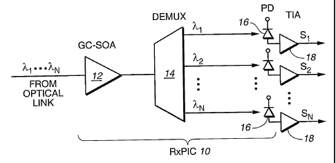
Reference is now made to Fig. 1 which illustrates one feature of this
invention. Fig. 1 is a
diagrammatic view of integrated optical components comprising the optical
receiver photonic
integrated circuit (RxPIC) 10 of this invention. RxPIC chip 10 comprises a
gain clamped
semiconductor amplifier (GC-SOA) 12 having an input at an input facet (not
shown) of chip
to receive, such as from an optical transmission link, multiplexed optical
data signals
k1 = = . kN for immediate amplification prior to signal demultiplexing. This
is an important
10 function in order to insure that the optical signal to noise ratio or OSNR
is maintained at a low
noise figure. More importantly, GC-SOA 12 is used instead of a SOA, such as
disclosed in
the M. Zimgibl et al. paper, supra. A GC-SOA is an amplifier in which feedback
is created
through an established laser cavity in the amplifier around the amplifying
medium so that
oscillation is generated inside the amplifier cavity at a predetermined
wavelength as defined
by a grating formed in the amplifier cavity. This device is, therefore, a
semiconductor laser
amplifier having a DFB laser cavity, although the lasing cavity could also be
a DBR lasing
cavity within the scope of this invention. The reasons why a GC-SOA is better
than a SOA in
this application is to provide a gain clamped signal to eliminate loss of gain
to higher
wavelength channel signals and also the TE/TM gain ratio is fixed due to the
presence of the
gain camp signal and, therefore, this ratio does not change due to power
variances in the input
channel signals.
As shown in Fig. 1, the output from GC-SOA is provided to an optical
demultiplexer
(DEMUX) 14 where the signal channels are demultiplexed and placed on DEMUX
waveguide
outputs as channel signals, X1...XN, to respective photodiodes 16
PD(1)...PD(N), which
produce electrical signals which are then initially amplified by low noise
figure,
transimpedance amplifiers (TIAs) 18 as is known in the art. The preferred
demultiplexer is an
arrayed waveguide grating because of its low insertion loss properties.
However, it is within %
the scope of this invention to also include as a demultiplexer, an Echelle
grating.
It is within the scope of this invention that, instead of employing an on-chip
optical
amplifier 12 as shown in Fig. 1, an off-chip fiber amplifier may be employed,
such as EDFA
12A illustrated in Fig. 67. As shown in Fig. 67, this monolithic RxPIC chip 10
would then be
comprised of integrated components comprising, for example, a demultiplexer 14
in the form
of an AWG, for example, and photodetectors 16(l) ... 16(N).
It is further within the scope of this invention that RxPIC 10 chip 10
primarily consists of
an AWG and an array of photodetectors which will be explained in more detail
later.
It is also with the scope of this invention that the primary components
comprising this
invention, to wit, a GC-SOA 12, demultiplexer 14 (preferably an AWG) and
photodetector
-11-
CA 02463545 2004-04-08
WO 03/102659 PCT/US02/32110
array 16 be of separate discrete optical elements. However, it will be
understood by those
skilled in the art the impact of their integration on a single InP chip to be
a highly desirable,
compact, cost effective and easily replaceable component as an optical
receiver system.
It is within the scope of this application that photodiodes 16 PD(l) ... PD(N)
may be
comprise of a PIN photodiode as shown in Fig. 25, or an avalanche photodiode
as shown in
Fig. 26, or a metal-semiconductor-metal (MSM) device comprising inter-
digitized contacts as
shown in Fig. 27. Examples of an avalanche photodiode are disclosed in pending
provisional
application, Serial No. 60/342,984, filed December 21, 2001, and entitled,
"InP-BASED
PHOTONIC INTEGRATED CIRCUITS WITH Al-CONTAINING WAVEGUIDE CORES
AND InP-BASED ARRAY WAVEGUIDE GRATINGS (AWGs) AND AVALANCHE
PHOTODIODES (APDs) AND OTHER OPTICAL COMPONENTS WITH AN InAlGaAs
WAVEGUIDE CORE", which application is incorporated herein by its reference.
Examples
of MSM photodetectors are disclosed in articles of B. D. Soole, et al.,
entitled, "Waveguide
MSM photodetector on InP", ELECTRONICS LETTERS, Vol. 24(24), 24 November,
1988;
"High-Speed Performance of InAlAs/InGaAs MSM Photodetectors at 1.3 m and 1.5
m
Wavelengths", IEEE Photonics Technology Letters, Vol. 2(8), August, 1989; and
"InGaAs
Metal-Semiconductor-Metal Photodetectors for Long Wavelength Optical
Communications",
IEEE Journal of Quantum Electronics, Vol. 27(3), pp. 737-752, March, 1991,
which articles
are incorporated herein by their reference.
Figs. 62A and 62B provide for alternative type of photodetectors that may be
employed on
RxPIC 10 as compared to the types that have been previously explained relative
to Figs. 25-27
and comprise high speed velocity-matched distributed photodetectors (VMDPs).
VMDPs are
optical waveguides upon which are fabricated a plurality of photodetectors
that are
interconnected with optical and coplanar electrical waveguides and their
quantum efficiency is
dependent upon the number of photodetectors deployed in an array along the
electrical
waveguides. "Velocity-matched" refers to matching the velocity of the RF
optics and RF
signal along the optical waveguides. Each of the photodetectors in the array
contribute
constructively to an optimum output so that all the photodetectors in the
array must operate in
phase with one another relative to any signal channel in order for an optimum
electrical
response to be produced. In Fig. 62A, each output channel on a waveguide 39
includes an
array of photodiodes 270 which produce an electrical signal proportional to
the amplitude of
the channel signal in a waveguide 39. The electrical signal is collected by a
separate
microwave transmission line 272 that is velocity matched to the optical
waveguide 39 and the
electrical signals are taken off of chip 10 at pads 274. See, for example, the
article of L. Y.
Lin et al., entitled "Velocity Matched Distributed Photodetectors With High-
Saturation Power
and Large Bandwidth", IEEE Photonics Technology Letters, Vol. 8(10), pp. 1376-
1378,
October, 1996, which article is incorporated herein by its reference. In Fig.
62B, TIAs 276
-12-
CA 02463545 2010-01-07
and limiting amplifiers 278 are integrated on RxPIC chip 10 employing InP-HBT
or InP-
HEMT technology.
Reference is now made to Fig. 63 which discloses another type of photodetector
that may
be deployed in this invention comprising traveling-wave photodetectors
(TWPDs). In Fig. 63,
the arrangement comprises a photodetector 280, such as a PIN photodiode,
fabricated at the
end of waveguide 39 from AWG 30. Photodetector 280 is central of a parallel
plate, co-planar
transmission line comprising signal line 284 and ground lines 286 providing
for a matched
electrical termination at the output end. As an example, see the article of
Kirk S. Giloney et
al., entitled "Traveling-Wave Photodetectors", IEEE Photonics Technology
Letters, Vol.
4(12), pp. 1363-1365, December, 1992.
As shown in Fig. 2, additional amplification of the DEMUX'ed channel signals
can be
provided with integrated semiconductor optical amplifiers (SOAs) 20 in the
optical
waveguides formed between DEMUX 16 and photodiodes (PDs) 16.
As illustrated in Fig. 3, there may be more than one GC-SOA 12A, 12B and 12B
at the
RxPIC input for purposes of redundancy so that the on-chip performance of
these respective
GC-SOAs 12A-12C can be checked relative to the ITU grid of the DEMUX 14 in
order that
the best performing GC-SOA can be selected, e.g., the one with the best gain,
saturated power,
noise figure, etc. characteristics. The number of SOAs 12 included on chip 10
is preferably in
the range of about 2 to 5 such devices. Three are shown in the illustration
here. However,
more such devices are preferred, such a sufficient number to cover or extend
slightly beyond
the spectral range for DEMUX 14 where the wavelength variation of the spectral
grid in the
fabrication of DEMUX 14 may be not be the same for all devices formed in the
same wafer or
for devices formed from wafer to wafer. In this manner, the yield of RxPIC
chips 10
obtainable from a wafer can be decisively increased. Once the best performing
GC-SOA is
selected, the input coupling of the channel signals from the fiber link can be
aligned and fixed
to the selected GC-SOA. The selection of performance is enhanced also by the
employment
of heaters 22 placed in close proximity to each GC-SOA 12A-12C so that the
response of the
individual SOAs 20 can be adjusted to better matched to the ITU grid of
optical DEMUX 14.
Reference is now made to Fig. 4 illustrating the plan view or layout of a more
detailed
form of RxPIC chip 10 of this invention which further includes input optical
mode adapters
(MAs) 24A, 24b and 24C for the respective GC-SOAs 12A, 12B and 12C as well as
respective output optical mode adapters (MAs) 26A, 26B and 26C. Passive MAs
24A-24C
permit multi-wavelength beam expansion into the GC-SOAs from the single mode
fiber
coupled to one of the selected inputs, while passive MAs 26A-26C permit beam
reduction to a
single mode passive waveguide 37 connecting the respective GC-SOAs 12 to DEMUX
14. It
is preferred that MAs 24 and 26 adiabatically increase and decrease the input
beam,
respectively, in order that the beam is gradually expanded and then contracted
for lowest
optical loss. Also, the use of MAs are critical from the standpoint of forming
a composite
-13-
CA 02463545 2004-04-08
WO 03/102659 PCT/US02/32110
beam of light that is circular and render it less critical in tolerances
relative to fiber alignment
of the fiber input to RxPIC 10 with regard to input MAs 24. Also, output MAs
26 provide for
matching the optical mode from SOAs 12 to DEMUX 14 to insure polarization
insensitivity is
preserved with low optical losses and lower optical back reflections such as
from downstream
optical components. More will be said about these mechanisms later. Also,
shown in Fig. 4
are the contact pads 28 at the output end of chip 10 for receiving the
respective electric signals
from PDs 16 for transfer off the chip to an RF submount board for electrical
domain
amplification and subsequent processing.
It would be best to have the alignment of the array of PDs 16 on chip 10 to be
out of direct
alignment of the axial optical path of GC-SOAs 12. Spontaneous emission (ASE
generated at
the selected GC-SOA 12 propagating through chip 10 will provide added noise to
photodetectors 16. A scheme to spare photoconductors 16 from this noise is
illustrated in Fig.
5, next to be discussed.
Reference is next made to Fig. 5 which illustrates in even more detail
embodiment of this
invention for RxPIC chip 10 comprising this invention. Chip 10 is formed in
the
InGaAsP/InP regime and, for example, may have dimensions of about 1.45 mm by
6.2 mm.
Chip 10 includes a plurality of input MAs 24A-24C to expand the input beam at
the channel
signal input to a selected GC-SOA 12A-12C, as previously explained, and the
channel signals
are reduced to single mode by a respective output MA 26A-26C. The input fact
to RxPIC chip
10 may include an AR coating, as may be the case of any of the other
embodiments disclosed.
The AR coating aids in coupling multiplexed channel signals into the chip as
well as prevents
internal backward reflections from occurring and interfering with the
operation of the chip,
particularly the operation of photodiodes 16. The signals are then provided,
via a passive on-
chip waveguide 37, to a vernier input of a first slab or free space region 32
of AWG DEMUX
30. It is preferred that the length of the MAs be as small as possible so as
not to add to
increasing the area real estate required for chip 10. The vernier input shown
here comprises
three different inputs to the input slab 32 of AWG 30 so that a best
operational match of GC-
SOA 12 to the wavelength grid of AWG 30 can be selected. Thus, through the
selection of
the best vernier input in the first order Brillouin zone and the best
performing GC-SOA 12, the
best wavelength grid alignment to AWG 30 can be selected that provides
optimized
wavelength matching and lowest coupling loss. This is shown in more detail in
Fig. 5A,
which is a bit exaggerated in scale to illustrate this invention. In Fig. 5A,
there are five GC-
SOAs 12A-12E shown integrated on chip 10 with their respective output
waveguides 37
comprising a group of vernier inputs 37V in the central portion of the first
order Brillouin
zone of slab or space region 32. Because fabricating techniques may not
precisely place the
amplifier waveguide input at the exact position desired at the slab 32 input,
the placement of a
plurality of waveguide inputs along the center of the first order Brillouin
zone forms a vernier
permitting the selection through signal testing of the respective GC-SOAs 12
to determined
-14-
CA 02463545 2010-01-07
which first order input provides the optimum performance in handing the
multiplexed channel
signals, such as in terms of signal separation, low optical noise and narrow
signal bandwidth.
While the best performing GC-SOA 12 may be on the wrong waveguide arm to the
input of
AWG 30 for best wavelength matching to the grid of the AWG, a lower
performance-GC-
SOA 12 may be chosen in combination with temperature tuning of AWG, via an AWG
heater
30A, to optimize the matching of the wavelength grid of AWG 30 to the selected
GC-SOA.
While other types of optical demultiplexers may be utilized in this invention,
such as an
echelle grating, a multichannel grating demultiplexer comprising wavelength-
select angled or
blazed gratings, a reflector stack filter, or multimode interference (MMI)
couplers.
A RxPIC chip 10 with a echelle grating type demultiplexer is shown in Fig. 56.
Chip 10
comprises an integrated photonic circuit that includes GC-SOA 12, echelle
grating 175 and
photodetectors 16(l)... 16(7). Grating 175 disperses the multiplexed signal
wavelengths
received from GC-SOA 12 into separate signals that are reflected back to
respective output
waveguides 176 and associated photodetectors 16. See, for example, the papers
of J. B. D.
Soole et at., entitled, '`WDM Detection Using Integrated Grating Demultiplexer
and High
Density PIN Array", LEOS 1992. Summer Topical Meeting Digest, pp. B7-B8, July
29, 1992
to August 12, 1992, Santa Barbara, CA; High Speed Monolithic WDM detector for
1.5 p.m
Fibre Band", ELECTRONIC LETTERS, Vol. 31(15), pp. 1276-1277, July 20, 1995;
and
"Monolithic InP/InGaAsP/InP Grating Spectrometer for the 1.48 - 1.56 mm
Wavelength
Range", Applied Physics Letters, Vol. 58(18), pp. 1949-1951, May 6, 1991.
A demultiplexer can also be comprised of a series of angled gratings each of
which has a
grating period designed to remove from the waveguide a selected wavelength
channel from
the propagating multiplexed channel signal. This type of demultiplexer is
illustrated in Fig.
68. RxPIC 10 comprises a GC-SOA 12 to receive the incoming channel signals,
ki...kN,
which provides signal amplification after which the signals propagate through
mode adaptor
26 and onto a single mode waveguide 182. Waveguide 182 contains a series of
angled or
blazed gratings 180(1)...180(N), one for each channel signal. Each grating
period is designed
to have a peak reflection wavelength equal to one of the signal wavelengths,
2, ...2 , so that
each of the signal wavelength, X. X2, ? 3, etc., is consecutively reflected
out of waveguide 182
to a corresponding photodetector 16(1)...16(N) at the same semiconductor layer
level in the
chip as waveguide 182. Photodetectors 16 may be formed along one edge of chip
10 to
transfer the detected signals off-chip. Each of the gratings 180(1)...180(N)
may be also
provided with a heater 184 in close proximity to a grating so that the
gratings 180 may be
individually tuned at the factory or in the field to insure that that their
reflection wavelength
peaks are at or very close to the respective: channel signal wavelength peak
for optimum
detection at a corresponding output photodetector 16. By the same token, if a
channel signal
or signals are slight off their peak wavelengths, the respective gratings 180
can be selectively
-15-
CA 02463545 2010-01-07
advantage of this embodiment as an optical demultiplexer is that the clamping
signal and any
ASE developed at the GC-SOA 12 is directed forward along waveguide 182 and out
of chip
providing for high OSNR in signal detection by photodetectors 16.
A reflector stack filter functioning as a demultiplexer may be of the type
that has plural
5 reflector surfaces that provide for successive reflection of peak
wavelengths comprising the
channel signal wavelengths spatially along the filter so that the spatial
array of demultiplexed
channels signals may be directed to an array of corresponding photodetectors
(see U.S. patent
6,111,674) or narrow band elliptical mirrors or elliptical Bragg reflectors of
the type disclosed
in the paper of Charles H. Henry et al., entitled "Four-Channel Wavelength
Division
10 Multiplexers and Bandpass Filters Based on Elliptical Bragg Reflectors",
Journal of
Lighiwave Technology, Vol. 8(5), pp. 748-755, May, 1990.
A multichannel grating reflector functioning as a demultiplexer is illustrated
in the article
of P. A. Kirby, entitled, "Multichannel Wavelength-Switched Transmitters and
Receivers
New Component Concepts for Broad-Band Networks and Distributed Switching
Systems",
Journal of fLightwave Technology, Vol. 8(2), pp. 202-211. February, 1990.
An MMI coupler device comprises a multi-mode slab waveguide, which can support
several modes, with N inputs (in the case here including demultiplexing only
one input is
needed) and M outputs and is based upon a self-imaging property wherein an
input field
profile is reproduced in a single or multiple images at periodic intervals
along the propagation
direction of the slab waveguide. See, for example, the articles of Lucas B.
Soldano et al.,
entitled, '`Optical Multi-Mode Interference devices Based on Self-Imaging:
Principles and
Applications", Journal of Lightwvave Technology, Vol. 13(4), pp. 615-627,
April, 1995, and of
K. Okamoto et al., entitled "Fabrication of Coherent Optical Transversal
Filter Consisting of
MMI Splitter/Combiner and Thermo-Optic Amplitude and Phase Controllers'",
ELEC'TRONIC
LETTERS, Vol. 35(16), pp. 1331-1332, August 5, 1999.
With respect to all of these different embodiments for an optical
demultiplexer, an AWG
device is preferred because of its better routing and filtering
characteristics. Reference is now
made to Fig. 5 where an AWG 30 is shown in RxPIC chip 10. As is well known in
the art, the
slab 32 provides for diffraction of a multi-wavelength signal beam into a
plurality of outputs
to waveguide arms 34, each having a different path length. The outputs of
waveguide arms 34
are coupled to a second slab or free space region 36 where the respective
channel wavelengths
are place respectively on a plurality of output passive waveguides such as
along the first order,
central Brillouin zone of slab 36. Each of these outputs in passive waveguides
39 from WAG
-16-
CA 02463545 2004-04-08
WO 03/102659 PCT/US02/32110
30 is coupled to a respective PD 16 and the electrical signal output of the PD
16 is placed on a
respective output signal pad 28 of chip 10.
GC-SOAs 12A-12C of chip 10 are provided with segmented electrodes or contacts
32, that
may take on a countless number of configurations, but only a few examples are
shown here
with respect to Figs. 5, 6, 9 and 10. In connection with GC-SOA 12A, two
segmented
electrodes or contacts 32A and 32B are shown approximately equal distance from
the ends of
the optical amplifier. These respective contacts 32A and 32B are respectively
coupled to
receive currents, I1 and 12- On the other hand, as shown relative to GC-SOA
12B, segmented
contacts 32A and 32B are positioned closer to the output end of the amplifier.
Conversely, a
multiple number segment contacts 32A-32E may be utilized such as shown in
connection with
GC-SOA 12C. Segmented contacts 32A-32E are respectively contacted to receive
different
currents 11-15. In each of these three different cases of GC-SOA contacts, it
can be that 11 > 12
in order to improve the noise figure (NF) of the amplifier. On the other hand,
if I2 > I1, then
better power saturation, PSAT, can be achieved. By placing the contacts closer
to the output of
the amplifier, such as shown in connection with GC-SOA 12B, improved
performance relative
to noise figure (NF) as well as saturation gain might be achieved. In this
connection, the
multiple array of segmented electrodes 32A-32E in GC-SOA 12C may be provided
with a
variety of distributions of applied current, for example a monotonically
increasing applied
current, I1-15, applied respectively to contacts 32A-32E, i.e., I1 < I2 < 13 <
14 < 15. or a
distribution that is relatively larger at both the input and output ends than
in the middle, e.g. I1
> 12 > 13, 13 < 14 < I5. The current distribution is optimized to provide the
best noise figure and
saturation power performance
RxPIC chip 10 may also have an open trough or layer barrier 38 formed in the
chip body
which, for example, extends into the substrate of the chip for the purpose of
blocking or
otherwise scattering stray light out of the chip, particularly stray light
(e.g. ASE) from GC-
SOAs 12, so that such stray light does not affect PDs 16, i.e., does not
interfere with the true
channel signal sensing to be accomplished by these photodiodes for
demultiplexed channel
signals received from AWG DEMUX 30. If barrier 38 is an open trough, it is
best that its side
surface 38A be somewhat rough so that stray light propagating to the trough
edge from the
direction of GC-SOA 12 will be scattered out by the rough side surface of the
trough and out
of chip 10. On the other hand, if barrier 3 8 is to be filed with a light
blocking or absorbing
material, a number of materials may be used, which may be semiconductor,
dielectric,
amorphous or polycrystalline in nature.
Lastly, the input surface of chip 10 is preferably coated at its input surface
11 with an
antireflecting (AR) material, as is known in the art, in order to increase the
input coupling
efficiency to the chip and also to eliminate spurious reflections from the
facet altering the
behavior of GC-SOA 12.
-17-
CA 02463545 2004-04-08
WO 03/102659 PCT/US02/32110
Reference is now made to Fig. 6 where the RxPIC layout provides for less
scattered light
interference between optical components but the compromise is that this
necessitates larger
chip real estate. However, the area real estate necessary for chip components
may be reduced
to some degree by fanning out the bonding pads 28 on chip 10, particularly for
PDs 16 so that
they are positioned along more than one edge of chip 10 as shown in Fig. 6,
compared to Fig.
5 where they are aligned only along one edge of the chip. Thus, RxPIC chip 10
in Fig. 6 is
larger than the RxPIC chip 10 shown in Fig. 5 and may be, for example, 4.3 mm
by 4.2 mm.
Also, further shown in Fig. 6 is a SOA 40 and an ASE filter 42 formed in each
of the output
waveguides 39 from AWG 30. SOAs 40 of selectively controlled, via an applied
positive
bias, or even negative bias to function as an absorber, to provide for
equalization in gain
across the demultiplexed channel signals emanating from AWG 30. Filters 42
have a narrow
bandwidth within the channel signal spectrum to filter out other wavelengths,
particularly
higher wavelengths of spontaneous emission or ASE generated in SOAs 40.
It should be noted in this embodiment as well as previous embodiments that GC-
SOAs 12
generate amplified spontaneous emission or ASE. Another reason why AWGs are
the
preferred choice for demultiplexing channel signals on-chip is because of the
narrow
wavelength filter quality of AWG 30 can filter out the clamping signal
associated with the
GC-SOA which are in the bandwidth of ASE.
It is desirous to keep photodetectors 16 positioned out of direct axial
alignment with the
GC-SOAs 12 so as to prevent spontaneous emission from these devices from being
detected
by PDs 16. This is accomplished by the placement of the outputs of GC-SOAs 12
not to be in
direct optical alignment with PDS 16. However, this is not always possible to
one hundred
percent because the chip size may become too large in the direction 44 so that
it is more apt to
break during processing and becomes more difficult to manage for placement in
a hermetic
package. In the embodiment of Fig. 6, therefore, a trough (not shown) may be
utilized in the
manner of trough 38 illustrated in Fig. 5.
As indicated in the previous embodiment, multi-segment SOA contacts 32 aid to
minimize
the total current drawn by these devices, particularly in the upstream portion
of the device
where the gain should be higher. Moreover, if the saturation power is not
required to be too
high, the full bias applied to reach saturation need not be applied at the
downstream end of
these devices. The last electrode segment 32C may, alternatively, be employed
to measure
photocurrent of the GC-SOA 12 to monitor its gain and correspondingly increase
or decrease
the gain as necessary to optimize the operation of the device.
Since the optical power increases from the upstream end towards the downstream
end of a
GC-SOA then the optimum use of pump current in a GC-SOA should increase
towards the
downstream end if it is desired to avoid saturation effects. This can be
accomplished in the
Fig. 6 embodiment by placing less bias on electrode segments 32A compared, for
example, to
segments 32B and 32C. Thus, for example, the applied bias may be controlled
such that I3 >
-18-
CA 02463545 2010-01-07
12 > I. Alternatively, as shown in Fig. 9, the electrode segments 44 may be
monotonically
increasing in size toward the downstream end of GC-SOA 12 so that for equal
biases the
currents will vary, such that resulting currents drawn via electrode segments
44A-44F, due to
their area, would be 44F > 44E > 44D > 44C > 44B > 44A. Another alternative is
shown in
Fig. 10 where electrode segment 46 is tapered so as to be monotonically
increasing in segment
contact area from the upstream end to the downstream end of the device. Thus,
monotonically
increasing current will be supplied along the length of GC-SOA 12.
A further embodiment relating to current control to GC-SOA 12 is shown in Fig.
1 1 where
a cross-section of GC-SOA 12 is shown, in particular at the region of the GC-
SOA at its
downstream end. In Fig. 11, GC-SOA 12 comprises a buffer layer 62 of n-lnP on
an n-InP
substrate 60 followed by a grating layer 64 of InGaAsP, which is also referred
throughout the
description in this application as a "Q" layer or "Q" multi-quantum well
region, meaning a
"InGaAsP quaternary" layer or region. Also, it should be realized that a semi-
insulating
substrate, such as InP:Fe or InP:O, may be used instead of semiconductor
substrate, e.g., n-lnP
with an appropriate change in metal contacting as is known in the art. Q layer
64 is followed
by an InP layer 66 that smoothes out the growth surface for the growth of the
amplifier active
region 65 which is Q layer or quantum well region. This is followed by the
growth of
confinement layer 68 of undoped or p-doped InP. At this point, the initial
MOCVD growth
process is completed, a selective etch is made to buffer layer 62, for
example, and a second
growth comprising the growth of current blocking layer 74 is accomplished
which may be, for
example, InP:Fe, InP:O or InP:O:Fe, followed by a selective etch though the
overgrown
blocking layer 72 to InP confinement layer 68. This isotropic etch step is
accomplished with a
tapered mask so that the width of opening 69 formed along the length of the GC-
SOA
monotonically increases from the upstream end to the downstream end of the
device, the
largest width being as shown in Fig. 11. Then, a third growth is accomplished
comprising
cladding layer 70 on p-lnP followed by the growth of the contact layer 72 p+-
lnGaAs. Thus,
the resulting structure is a tapered current channel formed along the optical
axis of GC-SOA
12 so that the gain created through contact layer 72 monotonic increases from
the upstream
end to the downstream end of the device.
Reference is now made to Fig. 7 which illustrates a plan view of a particular
embodiment
for GC-SOA 12 and its optically coupled MAs 24 and 26. The similar structural
device is
shown in the paper of P. Doussiere et al,., entitled "1.55 m Polarization
Independent
Semiconductor Optical Amplifier with 25 dB Fiber to Fiber Gain", IEEE
Photonics
Technology Letters, Vol. 6(2), pp. 170-172, February, 1994. This figure in
particular illustrates the waveguide layer of the device where the optical
mode of the
multiplexed signal is initially expanded in input MA 24, amplified in GC-SOA
12 (unlike
the device in the paper to Doussiere et al.) and then the optical mode is
converted
back to single mode via output MA 26 for proper mode entry into
-19-
CA 02463545 2010-01-07
waveguide 37 and AWG 30. The cavity of GC-SOA 12 includes a light feedback
mechanism
to provide a laser signal at a frequency not within the bandwidth of the
channel signals. As
will be seen later in Fig. 8A, the feedback mechanism may be a grating.
Another such
mechanism would be built-in mirrors at the laser signal wavelength at each end
of the GC-
SOA cavity.
Reference is now made to Fig. 7A showing another embodiment for GC-SOA 12 and
MAs 24
and 26. In this embodiment, RxPIC chip 10 includes an input waveguide formed
in the chip
for receiving the multiplexed channel signals, X ...? N, from an optical link
via optical fiber
46. To be noted is that input waveguide 48 is curved relative to input facet
52. Fiber 46 is
angularly disposed relative to input facet 52 and is aligned to optimize the
coupling of the
signal into input waveguide 48. It then is mode expanded via MA 24, amplified
by GC-SOA
12, mode contracted via MA 26 and propagates on waveguide 37 to AWG 30. In the
InP
regime, these waveguiding components 48, 24, 12, 26 and 37 may utilize a light
propagating
waveguide comprised of InGaAsP or Q, which is cladded by n-type and p-type InP
layers as
shown in the paper to P. Doussiere et al. The angularity of input waveguide 48
relative to a
normal to the input facet 52 may be several degrees, in the case here shown as
7 . Input facet
52 also includes an antireflecting (AR) coating 54 to reduce stray or
scattered light from
reflecting back into input waveguide 48. Also, the angularly disposed input
waveguide 48 at
7 further reduces input facet reflectivity. Curved waveguide 48 to facet 52
prevents optical
feedback into the cavity of GC-SOA 12. Also, undesired reflections are caused
from input
facet 52 where optical fiber 46 is butt coupled to RxPIC 10 and these
reflections can affect the
incoming signals, such as, changes in intensity, which is undesirable in DWDM
applications.
A further shape for GC-SOA 12 and its associated MAs 24 and 26 may be of the
type shown
in the paper to Hatakeyama et al., entitled, Uniform and High-Performance
Eight-Channel
Bent Waveguide SOA Array for Hybrid PICs", IEEE Pholonics Technology Lellers,
Vol.
13(5), pp. 418-420, may, 2001. The waveguides, comparable to waveguides 48 and
37, as
well as coupled MAs, comparable to MAs 24 and 26, are bow-shaped so that the
straight SOA
section and the MAs/passive waveguides are smoothly coupled by an 820 m
curvature. The
SOA in this paper, however, is not gain-clamped and is utilized in a different
application
(switching) and the SOA active layer and the MAs/passive waveguides are one
and the same
layers.
In Fig. 7B, GC-SOA 12 is also curved with expanding mode adaptor 24 provided
at input
facet 52 to receive the incoming multiplexed channel signals. The grating for
the laser signal
of GC-SOA 12 may be provided only in the downstream section 12G 1 or,
alternatively, could
be provided, as well, in the upstream curved section 12G2 where the gratings
in both sections
are normal to direction of light propagation and the pitch of the grating in
section 12G2 is
greater than that in section 12G 1. See U.S. patent 6,008,675, and Fig. 3.
-20-
CA 02463545 2010-01-07
There are different types of gain clamped-semiconductor optical amplifiers
that may be
utilized in connection with this invention. Fig. 12 shows a first and
preferred type comprising
a DFB type GC-SOA 70 which basically comprises a plurality of semiconductor
layers
deposited on an n-InP substrate 72. These layers, in sequence, comprise a n-
InP confinement
layer 74, a Q grating layer 76 within which is formed a periodic grating to
cause lasing at a
clamp signal frequency, an InP smoothing layer 78, an active region 80 such as
a plurality of
quantum well layers of InGaAsP, which also functions as the waveguide layer of
the device, a
p-InP confinement layer 82, a p+-InGaAs contact layer 84, followed by a metal
contact 86.
Carrier recombination occurs in active region 80 to provide for multiplexed
signal
amplification as well as lasing action at the clamping signal wavelength, 2.,,
for providing a
clamping gain function, which wavelength is within the gain bandwidth of SOA
70 but
outside the wavelength grid of wavelengths, X]...XN, to be amplified by the
SOA. See for
example, published patent application EP 0639876A 1, published February 22,
1995.
Fig. 13 illustrates another type of GC-SOA comprising a DBR type GC-SOA 90
illustrated in
Fig. 13, having a plurality of layers formed on a n-InP substrate 92
comprising, in sequence,
confinement layer 94, grating layer 96 with distributed feedback grating
regions 96A and 96C
and central gain region 96B, smoothing layer 98 of InP, Q region 100
comprising an InGaAsP
layer or quantum well layers of this quaternary, confining layer 102 of p-InP,
contact layer of
p+-InGaAs, and segment contacts 106A, 106B and 106C. See the article of D.
Wolfson et al.,
entitled, "Detailed Theoretical Investigation of the Input Power Dynamic Range
for Gain-
Clamped Semiconductor Optical Amplifier Gates at 10 Gb/s". IEEE Pholonic
Technology
Letters, Vol. 10(9), pp. 1241-1243, September, 1998. With respect to this
article, either a
DBR GC-SOA with active DBR grating regions or passive DBR grating regions may
be
utilized. In the case of a passive type, contacts 106A and 106C to the DBR
grating regions
would not be pumped. However, in the case of an active type, contacts to the
DBR grating
regions 106A and 106C would be pumped. The latter case is preferred because
the currents, Ii
and 13, can be varied to tune the period between these grating regions in
order to selectively
tune the laser clamping signal. In this manner, the tuning of the clamping
signal can be easily
accomplished outside of the amplification bandwidth of the incoming signals,
k, ...A.N, thereby
enhancing the manufacturing yield of chips 10 incorporating these types of
devices. Current
12 adjusts the gain of the SOA. Such an arrangement for adjusting the gain can
include the
adjustment of all three contacts 106A, 106B and 106C and also by providing a
difference in
the currents Ii and 12 with 11 remaining constant, for example. will also
adjust the gain of the
amplifier.
It is within the scope of this invention that grating regions 96A and 96C in
Fig. I I can be
chirped so that through the employment of multi-segment contacts 106A, 106B
and 106C the
-21-
CA 02463545 2004-04-08
WO 03/102659 PCT/US02/32110
tunability range of the clamping signal can be greater over a larger range of
tunable
wavelengths.
Fig. 14 illustrates a still further type of GC-SOA comprising, in this case, a
SOA 110.
SOA 110 is shown here as a discrete component but is integrated into RxPIC 10,
and is
provided at its input with an injected gain clamping signal along with the
multiplexed multi-
wavelength signals, X1...XN, from the optical link. The gain clamping signal
may be optically
coupled to the input of chip 10 from an external source or, alternatively, may
be integrated in
a separate region of RxPIC chip 10 and optically coupled into the input
waveguide, such as,
for example, waveguide 48 in Fig. 7A, into SOA 110. SOA 110 comprises n-InP
substrate
112 upon which is epitaxially deposited lower confinement layer 114 of n-InP,
waveguide
core and active region 116 of Q, either an InGaAsP layer or multiple quantum
wells of this
quaternary, upper confinement layer of p-InP 118, and contact layer 119 of p+-
InGaAs. In this
embodiment, the clamping signal can also be tuned or changed. Also, it is
within the scope of
this invention to also tune this clamping wavelength to be at a Raman
amplification
wavelength with counter propagating of the Raman signal so that it can be
coupled out of the
RxPIC chip 10 via its input port for coupling into the optical fiber link and
counter
propagating therein to amplify the incoming signals, X1...XN=
Reference is now made to Fig. 15 which is a further embodiment of a GC-SOA 11
OA that
may be integrated into RxPIC chip 10 comprising this invention. GC-SOA 110A
comprises a
vertical cavity surface emitting laser (VCSEL) having a n-InP substrate 112A
upon which is
epitaxially deposited (following the initial deposit of a n-InP buffer layer)
a stack of
semiconductor DBR layers comprising bottom mirror 127, confinement layer 116A
of n-InP,
Q waveguide layer 118A, spacer layer 120A of InP, active region 122 comprising
a Q layer or
a Q-QW region, confinement layer 124 of p-InP, a stack of semiconductor DBR
layers
comprising top mirror 128 and a contact layer 123 of P++-InGaAs. Bottom and
top DBR
mirrors 127 and 128 may be comprised of 20 to 50 layers of InAlGaAs layers of
alternating
different mole fractions, or alternating layers of InAlAs/InGaAs or
InAlGaAs/InP or
InGaAsP/InP. This is followed by the necessary metallization comprising p-side
metal
contact 125 and metal contact 129. Operation through current and bias of GC-
SOA 11OA
provides lasing action producing gain clamping signal 117A between mirrors 127
and 128
providing gain at active region 122 for amplification of the channel signals,
X1...XN,
propagating in waveguide layer 118A. An advantage of deploying VCSEL GC-SOA
110A is
that the portion of the gain of clamping signal 117A not utilized can exit the
chip via the top
or bottom of amplifier 110A since DBR mirrors 127 and 128 are not 100%
reflective. On the
other hand, amplifier 11 OA is more difficult to fabricate than many of the
other embodiments
disclose herein. There are several other ways of eliminating the unutilized
gain of the
clamping signal which will be described latter.
-22-
CA 02463545 2010-01-07
There is also a Mach-Zehnder (MZ) type of SOA that may be utilized in this
invention. In this
case, the clamping signal can be coupled into the MZ-SOA.
It should be noted that in all of the forgoing embodiments of this invention,
the gain clamping
signal can be either on the long wavelength (red) or short wavelength (blue)
side of the
bandwidth or wavelength spectrum of the multiplexed channel signals.
Reference is now made to Figs. 8A, 8B and 8C which respectively disclose
representative
InP-based embodiments, in cross-section, comprising a DFB GC-SOA 120, a
photodetector,
shown here as a PIN photodiode 16, and a grating arm 34 of AWG 30. In Fig. 8A,
DFB GC-
SOA 120 comprises a first epitaxial growth process on n-InP substrate 112 upon
which is
epitaxially deposited in sequence a n-InP buffer layer 124, a lower
confinement layer 126 of
n-InP, Q grating/waveguide layer 128 (bandgap of about 1.3), an InP spacer
layer 130
(bandgap of about 1.4), active/waveguide region of Q-QW layers 132 (bandgap of
about 1.5),
and upper confinement layer 134 of p-lnP. Next, a selective etchback is
performed with
masking of the yet to be defined current confinement region 129, followed by a
second
epitaxial growth process comprising blocking layers which comprise a first
layer 131 of n-InP
followed by semi-insulating (SI) layer 133 of InP:Fe, InP:O or InP:O:Fe, and a
third layer 141
of p-InP. Masking over the current confinement region 129 of the formed device
is removed
and a third epitaxial growth process is commenced comprising cladding layer
135 of p-InP,
followed by contact layer 136 of p+-InP, which may be optional here but is
desired elsewhere
in the integrated chip, and thence contact layer 138 of p+-InGaAs. Device 120
is completed
with p and n electrodes 138 and 139. The channel signals propagate along
active layer 132
with evanescent overlap with waveguide layer 128 and these signals absorb gain
and are
amplified. Layer 128 also includes a DFB grating 128A for generation of the
gain clamping
signal.
It should be realized that the fabrication of GC-SOA 120 is done in
conjunction with other
optical components included in integrated form on RxPIC 10. Thus, the
epitaxial fabrication
sequence in the description here may be modified or include other steps so
that the layers and
structures of such components can be also be added or otherwise realized. This
same
statement also applies relative to the structures shown in Figs 8B and 8C.
In conjunction with the GC-SOA 120 of Fig. 8A, reference is now made to Figs.
31 and 32
which illustrate input mode adaptors or converters 24 that may be employed for
GC-SOA 12
or 120. In this connection, with reference to Fig. 31, the mode adaptor taper
24 is in the
vertical plane of PIC chip 10 whereas, in Fig. 32, the mode adapter 24 is
tapered in the
horizontal plane of PIC chip 10, i.e., in the plane of its as-grown layers. In
Fig. 31, generally
the same layers are shown as in the case of previously described Fig. 8A.
However, with a
selective masking technique, such as selective area growth (SAG), taper 24 may
be formed in
Q active region 132 during its growth to provide for an adiabatic expansion of
the input light
comprising channel signals, a,i ...2 . In this connection, see U.S. patent
6,141,477.
-23-
CA 02463545 2010-01-07
Patent `477 illustrates such a taper at the output end of an active region
rather then the input
end of an active region. Such an output taper can be also employed at the
output end of GC-
SOA 12 of Fig. 31.
In Fig. 32, the input tapered mode adapter 24 is shown in the horizontal
plane. In fact,
tapering can be provided in both the vertical and lateral directions to
provide an input or
output mode adapter 24 or 26 that adiabatically transform the input or output
light as taught in
U.S. patent 6,174,748 relative to output light. In patent `748, the purpose is
to produce an
output beam of substantially circular mode profile, which need not be the case
here as long as
the multiplexed channel signals are adiabatically converted to single mode.
Reference is now made to Fig. 8B which illustrates a cross-section of a
photodetector
that may be utilized in RxPIC chip 10. Photodetector 140 is a PIN photodiode
comprising
multiple epitaxially deposited layers, some of which are not necessary to its
operation but
present because of their necessity for other optical component(s) on the same
monolithic chip
10. The structure comprises, as is the case of GC-SOA 120, a first epitaxial
growth process of
n-InP substrate 122 upon which is epitaxially deposited in sequence a n-InP
buffer layer 124,
a lower confinement layer 126 of n-InP, Q layer 128 (bandgap of about 1.3 with
no grating
128A provided in this portion of the chip), an InP spacer layer 130 (bandgap
of about 1.4),
active/waveguide region of Q-QW layers 132 (bandgap of about 1.5), and upper
confinement
layer 134 of p-InP. Next, a selective etchback is performed with masking of
the yet to be
defined current confinement region 129, followed by a second epitaxial growth
process to
form current blocking layers comprising a first layer 131 of n-InP followed by
SI layer 133 of
InP:Fe, InP:O or InP:O:Fe and a third layer of p-InP. Masking over the current
confinement
region 129 of the formed device is then removed and a third epitaxial growth
process is
commenced comprising cladding layer 135 of p-InP. This is followed by the
deposition of
contact layer 136 of p+-InP and dielectric passivation layer 137. Contact
layer 136 is defined
by dielectric layer 137 which may be SiO2 or other such dielectric. The device
is completed
with a p-side metal contact 138 and a n-side metal contact 139. It should be
noted that GC-
SOA 120 is substantially the same as PIN photodiode 140 except that waveguide
layer 128
contains no grating at photodiode 140. Q layer 128 at photodiode 140 functions
as a carrier
depletion device by being reversed biased and generating a current signal
proportional to the
light entering the photodiode. Also, as will be realized from the previous
description of
RxPIC chip 10, there are N such photodiodes 140 (or 16) formed on the chip.
Reference is now made to Fig. 8C which illustrates the epitaxially deposited
layers for
AWG 130 such as AWG arrayed arms 34 as well as representative of cross-
sections of input
and output waveguides 37 and 39. Fig. 8C represents an exemplary cross-section
of any of
these waveguide structures comprising AWG 130. The slab or space regions 32
and 36 of
AWG 30 would have the same composite structure except the waveguiding region
would have
-24-
CA 02463545 2004-04-08
WO 03/102659 PCT/US02/32110
a larger extent in the lateral direction. As in the case of the optical
components 120 and 140
in Figs. 8A and 8B, a first epitaxial growth process on n-InP substrate 122
comprises epitaxial
deposition, in sequence, a n-InP buffer layer 124, a lower confinement layer
126 of n-InP, Q
waveguide AWG layer 128 (bandgap of about 1.3 with no grating in this portion
of the chip),
an InP spacer layer 130 (bandgap of about 1.4), active region of Q-QW layers
132 (bandgap
of about 1.5 but having no direct function in AWG 30), and upper confinement
layer 134 of p-
InP. Next, a selective etchback is performed with masking to define waveguide
structure 127,
followed by a second epitaxial growth process comprising cladding layers (in
previously
described structures of Figs. 8A and 8B functioning as blocking layers)
comprising a first
layer 131 of n-InP followed by SI layer 133 and a third layer 135 of p-InP. It
is within the
scope of this invention that waveguide 127 be not covered, i.e., it can be an
air-exposed
waveguide or, alternatively, other layers may be utilized for burying
waveguide 127, such as,
Si02, glass (silica), BCB, ZnS or ZnSe as examples.
The preceding described embodiments of Figs. 8A (GC-SOA), 8B (PD) and 8C (AWG)
are examples of buried types of devices. On the other hand, these devices can
be deep ridge
waveguide devices as illustrated, for example, in Figs. 65A, 65B and 65C. GC-
SOA 330 in
Fig. 65A, along with AWG 350 in Fig. 65B, comprise a n-InP substrate 332 upon
which are
epitaxially deposited n-InP confinement layer 344, Q-grating/waveguide layer
336 (with
grating layer 336A and smoothing layer 336B), and undoped InP layer 338. This
is followed
by the growth of active region 340 in GC-SOA 330 employing selective area
growth (SAG) so
as to taper this layer at 331 as shown in Fig.65C. This is followed next with
the growth of p-
InP confinement layer 342 over both GC-SOA 330 and AWG 350. Then an etchback
is
performed to form the deep ridge waveguide structures as shown in Figs. 65A
and 65B. Note
that the ridge is formed back through the waveguide core 336 to provide for
birefringence at
the AWG and ease of manufacturability, i.e., providing for less epitaxial
growth steps. These
structures may be exposed to air or covered with a high refractive index
material such as BCB,
ZnS or ZnSe.
To be noted in Fig. 65C, the waveguide layer 336 is continuous. However,
through
several epitaxial growth steps, the regrowths provide for lateral guiding with
an index step
optimized for birefringence at the AWG and single mode guiding at the GC-SOA
or the
photodetector. In this connection, reference is now made to Fig. 66. Fig. 66
shows a
longitudinal cross-section of RxPIC 10 comprising input mode converter 400, GC-
SOA 360,
AWG 380 and PIN photodetectors 390(N). A typical process for fabrication of
this structure
is a first growth process comprising the deposition of a n+-InP buffer layer
364 followed by
the deposition of a Q-grating layer 366, followed by an n-InP cap or stop etch
layer (not
shown due to subsequent removal). Next, a selective dry etch employing a
photoresist mask is
made in Q layer 366 to form DFB grating 367 for GC-SOA 360. Next, a second
growth
process is initiated comprising an undoped-InP planarization layer 368 to
planarize over
-25-
CA 02463545 2004-04-08
WO 03/102659 PCT/US02/32110
grating 367. This is followed by a third growth process comprising the
deposition of Q-
waveguide layer 370 and thence an n-InP cap or stop etch layer (not shown due
to subsequent
removal). Then a photoresist mask is applied to the area of AWG 380 and the
AWG is
defined via selective etching. Then, waveguide layer 370 over the regions
comprising GC-
SOA 360 and PIN photodetectors 390 are etched away. This is followed by a
fourth epitaxial
growth process for overgrowing the grating 367 as well as forming active
region 374 for both
GC-SOA 360 and PIN photodetector 390. First, an undoped InP layer 372 is
deposited
followed by a Q-active layer or MQW active region 374, followed by p-InP layer
376 and
contact layer 378 of pt-InGaAs. These layers 372, 374, 376 and 378 are then
etched over
mode converter 400 and AWG 380. Subsequent processing provides for a buried
waveguide
structure such as shown in Figs. 8A, 8B and 8C or a ridge waveguide structure
such as shown
in Figs. 65A and 65B. The etched regions 382 over mode converter 400 and AWG
380 may
be overlaid, for example, with InP:Fe, InP:O, BCB, ZnS or ZnSe. Arrow lines
385 in Fig. 66
shows the path of the channel signal mode as it propagates through the one
illustrated signal
channel of RxPIC 10.
Figs 16-22, 37 and 54 relate to various ways of either eliminating the
amplified
spontaneous emission (ASE) or residual laser gain clamping signal, or both,
from RxPIC chip
10. The residual gain clamping signal and ASE generated by the amplifying
function of GC-
SOA 12 or 120 is undesirable on chip 10 as it will interfere with the accurate
detection
functioning of photodiodes 16 or 120. When current is injected into GC-SOA 12
or 120, ASE
is emitted which is optical noise that interferes with the detection response
of photodetectors
16 as well as providing reflected light back into GC-SOA 12. Also, the DFB
grating
generated laser light to maintain the gain of GC-SOA 12 is not totally
utilized and, therefore,
propagates out of the amplifier to AWG 30. These figures illustrate approaches
to eliminate
this noise from RxPIC chip 10.
In Fig. 16, reliance on AWG 30 per se to filter out this noise is selected. In
the case here,
the AWG 30 must be designed to function as such a filter so that the cone
filter function is
limited strictly to wavelengths within the wavelength grid of the channel
signals.
Wavelengths outside this spectrum, such as ASE at higher frequencies or a
laser clamping
signal at a higher or lower wavelength not within this spectrum, is rejected
by the narrow band
filtering of AWG 30. In this case, AWG 30 must be designed to have a large
free spectral
range (FSR) to filter out the GC-SOA clamping wavelength signal.
As illustrated in Fig. 16A, the input waveguide 37 from GC-SOA 12 can be
provided with
a high angular bend at 37A along which the signal wavelengths can be guided
but not the
higher wavelengths of ASE or of a gain clamping signal if of sufficiently
higher wavelength
than that of the channel signal spectrum. Otherwise, where the laser gain
clamping signal is a
shorter wavelength than the channel signal spectrum, other means may be
necessary to
remove this signal from chip 10.
-26-
CA 02463545 2004-04-08
WO 03/102659 PCT/US02/32110
The free spectral range (FSR) of AWG 30 can, thus, be designed so as to filter
the gain
clamping signal propagating from GC-SOA 12 to AWG 30. If the wavelengths of
the modes
are very different, then the FSR of AWG 30 will have to also be large as well.
This can
therefore become a design constraint for the AWG. Thus other measures will
have to be taken
to rid the RxPIC chip 10 of this residual clamping signal, which is to be
described in several
subsequent embodiments.
Fig. 17 illustrates another way of filtering out ASE and the laser gain
clamping signal. In
this illustration, a bank of on-chip SOAs 31(1)...31(N) are integrated in each
of the output
waveguides 39 of AWG 30 to provide immediate gain to the demultiplexed channel
signals
which have experienced some insertion loss. These SOAs 31 are followed by in-
line filter
devices 33(l)...33(N) which may be on-chip angled or blazed gratings with
broadband
reflective gratings within the bandwidth of the clamping signal and ASE to,
not only eject the
ASE and clamping signal light from GC-SOA 12 from chip 10, but also eject the
ASE
generated by SOAs 31. Thus, these 'unwanted wavelengths which are noise are
eliminated
from proceeding on with the demultiplexed channel signals to photodetectors
16(l) ... 16(N).
Fig. 18 is a further embodiment for rejection of ASE and the residual gain
clamping signal
employing architecture similar to Fig. 17 except that the input amplification
to the multiplied
channel signals is a Raman or a rear earth fiber amplifier 35, such as an
EDFA, as opposed to
the employment of GC-SOA 12 or 120. Here, instead of on-chip initial
amplification via GC-
SOA 12 of the multiplexed channel signals, an off-chip booster fiber amplifier
35 is utilized.
(This is similar to Fig. 67, previously described). In the case here, SOAs
31(1)...31(N),
shown in Fig. 18, are optional. In-line filters 33(l)...33(N) each have a
filter band that passes
the demultiplexed channel signal but ejects the ASE and the residual clamping
signal from
chip 10. As shown in the embodiment of Fig. 19, no initial booster
amplification of the
multiplexed channel signals may be necessary so that, after channel signal
demultiplexing, the
individual channel signals may be amplified via SOAs 31(1)...31(N) and the ASE
and other
optical noise removed by in-line filters 33(l) ... 33(N) formed on chip 10.
Alternatively, as
shown in Fig. 19A, in a side view of RxPIC chip 10, output waveguides 39 from
AWG 30
include SOAs 20(N) which have a design essentially the same as a PIN
photodiode, such as
the photodiode 140 in Fig. 8C. SOAs 20(N) are inserted in each waveguide 39 to
provide for
channel signal amplification due such as to insertion loss. The amplified
channel signal then
proceeds into a respective angled grating 183(N) which functions as a narrow
passband filter
for reflecting the channel signal upwardly or transversely of PD 16. Grating
183(N) is
transparent to the ASE and other optical noise such as residual clamping
lasing signal so that
these different wavelengths exit the chip as shown at 185.
Reference is now made to Fig. 20 illustrating a still further way of rejecting
ASE and the
residual clamping signal from RxPIC chip 10. In this case, compared to the
embodiment of
Fig. 19A, the angled or blazed grating filter 33A here is deployed on the
input side of AWG
-27-
CA 02463545 2004-04-08
WO 03/102659 PCT/US02/32110
30 rather on its output side where a single grating filter 39 is designed to
reflect the bandwidth
spectrum 37A of the multiplexed channel signals. The ASE and clamping signal
are outside
this spectrum and, therefore, are transparent to filter 39 and, as a result,
are transferred through
the filter and out of chip 10 as shown at 185. A heater 33B may be associated
with filter 39 to
tune the bandwidth of the grating to better match the wavelength spectrum of
the channel
signal grid to the wavelength grid of AWG 30.
Fig. 21 illustrates another embodiment for extraction of the ASE noise from
chip 10 by
employing a Mach-Zehnder interferometer (MZI) 41 in chip 10 between GC-SOA 12
and
AWG 30. Since spontaneous emission from GC-SOA 12 is not coherent, such
emission
cannot be guided through MZI 41 and, therefore, functions as a filter for
receiving only
coherent channel signal wavelengths. The residual clamping signal can be
filtered by AWG
30, as in the embodiment shown in Fig. 16 or by the employment of angled
grating filters
31(1) ... 31(N) of Figs. 17-19.
In Fig. 22, an additional AWG 43 is employed as a filter mechanism for ASE and
the
residual gain clamping lasing signal. In this embodiment, the channel signals,
2 ...2 , are
deinultiplexed via AWG 30 and passed along output waveguides 39 through SOAs
31(l) ... 31(N), to cover for insertion loss, to NxN AWG 43 which provides a
narrow signal
passband rejecting any wavelengths outside the channel signal spectrum. The
channel signals
are then forwarded via waveguides 39A to their respective photodetectors 16(l)
... 16(N) for
optical to electrical signal conversion.
In Fig. 33, the residual gain clamping signal is removed by forming in the AWG
input
waveguide 37 from GC-SOA 12 a higher order angled or blazed grating 170 which
deflects
the higher or lower wavelength gain clamping signal, outside of the wavelength
spectrum of
the channel signals, out of RxPIC chip 10. Grating 170 can be part of GC-SOA
12. The
filtering out of the ASE in this embodiment would be accomplished in AWG 30 as
described
in the embodiment of Fig. 16. It is important that waveguide 37 be single mode
so that
grating 170 functions to eject the gain clamping signal from chip 10.
Fig. 34 is similar to the embodiment of Fig. 33. In the plan view of Fig. 34,
InP-based
RxPIC chip 10 comprises a GC-SOA 12 with an output coupled to a mode adapter
26 and a
waveguide 182. Waveguide 182 includes higher order grating 180 with an
integrated heater
184 and PIN photodiode 17 positioned in the same planar level to receive light
reflected from
grating 180. In the case here, the grating 180 has a peak wavelength that is
substantially the
same as the peak wavelength of the residual gain clamping signal generated by
GC-SOA 12.
The residual gain clamping signal is, therefore, deflected out of waveguide to
PIN photodiode
17 where it is detected and provides an electrical signal off-chip to monitor
the optical
characteristics of the gain clamping signal, such as, for example, its
intensity and wavelength
so that adjustments can be made, if necessary, to the applied bias of GC-SOA
12.
-28-
CA 02463545 2004-04-08
WO 03/102659 PCT/US02/32110
Fig. 35 is similar to Fig. 34 except that it is a view perpendicular to the
view of Fig. 34 and
illustrates, in cross-section, angled grating filter 180 in waveguide 182. A
lateral waveguide
188 is provided in the same as-grown layer as waveguide 182 to direct the
residual gain
clamping signal laterally to an etched trough or groove 187 formed in InP chip
10. Trough
187 has an angled surface at 45 with a deposited reflective surface 189
formed on the angled
surface to reflect, along its length, the gain clamping signal upwardly at 50
(or possibly
downwardly depending at what vertical position photodiode 17 is integrated
into chip 10) to
an optical aligned photodiode 17 integrated in chip 10. Trough 187 may be
etched by
employing RIE. The space of trough 187 may be filled with air or contain some
others low
refractive index medium.
Instead of the integrated photodiode 17 being directly vertical (Fig. 35) or
directly lateral
(fig. 34) of clamping signal filter 180, photodiode 17 can be offset
transversely in chip 10
from the position of grating filter 180 as illustrated in Fig. 36. Also,
instead of photodiode 17
being directly above or transversely of waveguide 182, photodiode 17 can be
positioned
below waveguide 182, as shown in Fig. 37, and the reflected light from angled
grating filter
180 is directed downwardly at an angle, employing a second order or higher
order integrated
grating 183 to reflect the residual clamping signal downwardly to integrated
PIN photodiode
17. Such a second order grating 183 can be in the same semiconductor layer in
which filter
180 is formed or in a different or separate semiconductor layer.
A final approach for removing the residual gain clamping lasing signal is to
employ this
signal for pre-amplification of the oncoming channel signals, provided that
the gain clamping
signal is also chosen to be within the absorption spectrum of the channel
signals. This
illustrated in Fig. 54 where the gain clamping is reflected back to mode
adapter 26 and
propagates out of the front facet of chip 10, indicated as 2 R, and into the
fiber link to counter-
propagate in the link. With 2R designed to be within the absorption bandwidth
of the
incoming channel signals, these signals will receive gain from its counter-
propagation. Rather
than a built-in reflector at the downstream end of GC-SOA 12, a quarter
wavelength shift to
the channel signal can be provided in the grating of GC-SOA 12 or a multiple
of that
wavelength over 4N, so that most of the power of the gain clamp signal not
utilized in the
amplifier will be directed out of the back or input port of chip 10 into the
fiber link.
In connection with the foregoing embodiment of Fig. 54, it is within the scope
of this
invention to provide on-chip laser pumps to provide for counter-propagation of
gain into
optical link to provide for initial amplification of the incoming channel
signals. This is
illustrated in the embodiments of Figs. 44 and 45. In Fig. 44, an on-chip
semiconductor
Raman pump laser 230 is provided at one of the remaining first order outputs
or higher order
Brillouin zone outputs of AWG 30 to provide counter propagating signal, 2 R,
through AWG
30 and GC-SOA 12 into the fiber link to provide for pre-amplification of the
incoming
channel signals. Such a pumping signal is transparent to the operation of GC-
SOA 12.
-29-
CA 02463545 2004-04-08
WO 03/102659 PCT/US02/32110
Alternatively, as shown in Fig. 45, an on-chip semiconductor Raman pump laser
232 could be
coupled into AWG input waveguide 37 to provide counter propagating signal, 2
R, through
SOA 12A into the fiber link to provide for pre-amplification of the incoming
channel signals.
Note here, that an SOA 12A is denoted rather than a GC-SOA since the Raman
lasing pump
laser signal can provide the on-chip gain clamping. Such Raman pumps could be
provided at
both such locations if desired. Also, and importantly so, it should be noted
that Raman pump
laser 232, whether an on-chip semiconductor Raman laser or off-chip Raman
fiber amplifier
coupled in a waveguide 39 of AWG 30 or waveguide 37, can be deployed instead
of having
an on-chip GC-SOA 12 or SOA 12A so that RxPIC chip 10, in this embodiment,
would be
comprised of Raman pump laser 232, AWG 30 and photodetectors 16(l) ... 16(N).
Reference is now made to Fig. 46, which discloses an on-chip signal monitoring
circuit
and transmitter laser for providing a service channel signal, ks. Electro-
optical circuit 234 is
coupled to one of the first order outputs or higher order Brillouin zone
outputs of AWG 30
and monitors the channel signals, via AWG output 233, for their peak
wavelength value to
determine if the channel signals are on the peak wavelengths and, if not, to
provide digitized
information in service channel signal, 2 s, back to a correspondent optical
transmitter about the
quality of the channel signal wavelengths relative to the standardized
wavelength grid at the
optical transmitter. As shown alternatively in Fig. 47, such an on-chip
electro-optical circuit
236 may also be provided with its input 235 into waveguide 37 to counter-
propagate service
channel signal, 2 s, through GC-SOA 12 and into the optical link.
In connection with circuit 234 or 236 of Figs. 46 and 47, reference is now
made to Fig. 64
illustrating an application of these types of circuits in an optical
communication system. The
system shown in Fig. 64 comprises an optical transmitter PIC (TxPIC) chip 300
optically
linked in an optical point-to-point transmission system via optical link 288
to RxPIC chip 10.
TxPIC comprises a plurality of integrated components in plural paths to an AWG
multiplexer
310 where each such path includes a DFB laser source 302, an electro-optical
modulator 306
and a SOA 308 (optional) coupled to a first order input of AWG 310. Each laser
source 302 is
operated cw at a designated peak wavelength corresponding to a standardized
grid, such as the
ITU grid. The output of each laser source 302 is modulated with an information
signal at its
respective modulator 306. Modulator 306 may be, for example, a semiconductor
electroabsorption (EA) modulator or a Mach-Zehnder (MZ) modulator as known in
the art.
The modulated signal may then be provided with gain via SOA 308. SOAs 308 are
optional
and are preferred not to be an on-chip optical component because the overall
power
consumption of TxPIC chip 300 will be less without them since most of the on-
chip power
consumption will come from the operation of SOAs 308. In the absence of SOAs
308, DFB
sources 302 will have to be operated at higher thresholds and operating
currents. The output
of AWG multiplexer 310 is coupled off-chip to optical link 288.
-30-
CA 02463545 2010-01-07
In order to operate TxPIC chip 300 in a stabilized manner, each DFB source 302
is
provided with a corresponding, integrated heater 304 and AWG 3 10 is provided
with TEC
310A. A small sample of the multiplexed channel signal output from AWG 310 is
provided
through a 1% tap, for example, and is provided as an electrical signal input,
via optical to
electrical domain conversion at on-chip PD 312, on line 311 to programmable
logic controller
(PLC) 316. PLC 316 discriminates among the different channel signals, X1...?
N, to determine
if the operating wavelengths of DFB sources are at their desired wavelength
peaks as
determined by reference to a peak wavelength reference memory. This
discrimination process
can be carried out by employing dithering signals on the modulated channel
signals providing
each such signal with an identification tag. As a result, each of the channel
signals can be
separated and analyzed as to its wavelength to determine if it is at a proper
wavelength
relative to a standardized grid, such as the ITU grid. Such a discrimination
scheme is
disclosed in US Patent No. 7,079,715, and entitled PHOTONIC INTEGRATED CIRCUIT
(TXPIC) CHIP ARCHITECTURES AND DRIVE SYSTEMS AND WAVELEGNTH
STABLILIZATION FOR TXPICS. If the peak wavelength of any particular DFB laser
source 302 is off, its operating wavelength is corrected to the desired peak
grid wavelength by
a signal provided from PLC 316 to heater control circuit (HCC) 320 which
provides a
temperature control signal to a corresponding laser source heater 304 for
increasing or
decreasing the operating temperature of its DFB laser source 302 by an amount
necessary to
increase or decrease its operating wavelength to be substantially the same as
desired and
stored peak wavelength.
The temperatures of DFB laser sources 302 are not monitored but the
temperature of
AWG is monitored with a thermistor 313 which provides PLC 316 current
information of the
AWG ambient temperature via input 3 15. PLC 316 can then provide a control
signal to heater
control circuit (HCC) 3 18 to provide a temperature control signal to TEC 310A
to increase or
decrease the ambient temperature of AWG 310. In this manner the wavelength
passband grid
of AWG 3 10 may be shifted and adjusted to optimize it to be as close as
possible to the
standardized grid and the wavelength grid of DFB laser sources 304.
Also, the input side of AWG 310 includes a port 317 relative to a higher order
Brillouin zone of the input side of AWG 310 for the purpose of receiving a
service signal, 2L .
from RxPIC 10 via optical link 288, which is explained in further detail
below. This service
signal is demultiplexed by AWG 3 10 and provided on port 317 as an output
signal and thence
converted to the electrical domain by integrated, on-chip PD 3 14. The
electrical signal from
PD 314 is taken off-chip and provided as an input 3 19 to PLC 316.
At RxPIC chip 10, AWG demulti~plexer 30 includes higher order Brillouin
zone outputs 289A and 289B to receive respective channel signals, such as, for
example, X and 42 or any other such signal pairs, in order to determine if
their grid wavelengths are off the desired peak
-31-
CA 02463545 2004-04-08
WO 03/102659 PCT/US02/32110
wavelength and, if so, by how much. Also, using these two channel signals as a
wavelength
grid sample, a determination can be made as to whether the AWG wavelength is
shifted and,
if so, by how much. Photodetectors 290A and 290B provide an electrical
response to optical
signals on outputs 289A and 289B which signals are provided on lines 291A and
291B to PLC
292. These PDs 290A and 290B are sensitive to the peak optical responses of
these signal
outputs and can be deployed in the electrical domain to determine if their
peak wavelengths
are off a desired peak wavelength. Also, if the delta shift, 8, of both is
approximately same
amount and in the same direction (both either a red shift or a blue shift
relative to their desired
wavelength peak), this delta shift is indicative that a shift in the
wavelength grid of either Rx
AWG 30 or possibly Tx AWG 306 has occurred. In these cases, PLC 292 can first
make
adjustment to the RX AWG grid via heater control circuit (HCC) 294 via line
295 to Rx TEC
30A to either increase or decrease the ambient operating temperature of AWG 30
to shift its
wavelength grid either to the longer or shorter wavelength side based on the
determined delta
shift. If this adjustment does not resolve the issue, then data relating to
either the DFB
channel signal wavelengths or the Tx AWG wavelength gird being offset from its
desired
setting can be forwarded over optical link 288 as a service channel signal, 2
, for correction at
the transmitter end. In these circumstances, PLC 292 can forward such
wavelength and grid
correction data as a service channel signal, 2 s, via an electrical correction
data signal on output
line 293 to service signal modulator 294, which may be comprised of an on-chip
integrated
DFB laser and EO modulator, to provide this signal through AWG 30 and counter
propagation
via optical link 288 to TxPIC 300. This service channel signal, ks, is then
demultiplexed via
AWG 310 and provided on higher order output 317 to PD 314. The electrically
converted
service signal data is deciphered by PLC 316 which makes a correction to the
operating
wavelength of a DFB laser source 302 via HCC 320 and/or makes a correction to
the
wavelength grid of AWG 310 via HCC 318.
Reference is now made to Fig. 69 where the RxPIC chip 10 and the TxPIC chip
300 of
Fig. 64 are deployed as an optical-to-electrical-to-optical (OEO) converter
400 for optical
signal regeneration in an optical transmission link. As shown in Fig. 69, the
incoming
multiplexed channel signals, /%,...2 , are received by RXPIC chip 10 from
optical link 408,
demultiplexed and converted into corresponding electrical channel signals and
provided
through low impedance coupling lines 403 to electronic regenerator 401
comprising a
plurality of circuits 402, 404 and 406, which may be comprised of a chip set
for each
demultiplexed electrical channel signal received from RxPIC 10. Circuit 402
comprises a
transimpedance amplifier and a limiting amplifier. Circuit 404 comprises
retiming and
reshaping circuit where the bit clock is extracted from the signal to reclock
the signal and
regenerate the channel signal. The regenerated electrical channel signal may
be further
amplified via circuit 406 and provided as an output on low impedance lines 407
to the electro-
optical modulators 306 of TxPIC chip 300 where the corresponding optical
signals are again
regenerated, the plural channels are multiplexed via AWG 310 and provided as
multiplexed
-32-
CA 02463545 2010-01-07
channel signal, on optical link 410. OEO converter 400 has the advantage of
being
cost effective, compact, easily field-replaceable compared to previous OEO
converters and
eliminates of the problems of optical-to-optical converters comprising erbium
doped fiber
amplifiers (EDFAs), functioning as line amplifiers, that need continuous
attention relative to
saturation where if the input signal power increases or decreases, the
amplifier gain drops or
increases. Also there is a problem of gain nonflatness across the channel
signal wavelength
band so that gain equalization techniques need to be provided. Also, these
optical line
amplifiers, while being the choice today for transmission line optical signal
amplification,
they are not as compact or readily replaceable as converter 400 particular
when changes are
made to increase the number of multiplexed channels and traffic to carried
over an optical
link. OEO converter 400 of Fig. 69 eliminates this problems and considerations
particularly
since the converter can be easily swapped in between optical links 408 and 410
with a
converter having larger channel capacity.
An important feature of RxPIC chip 10 is the monolithic incorporation of
optical components,
in particular GC-SOA 12 and AWG 30, which can provide polarization independent
gain to
the channel signals and function as a polarization insensitive waveguide
grating router or
demultiplexer. In GC-SOA 12, either the stable lasing in the TE mode or TM
mode to provide
the DFB clamping signal is preferred. It should be stable over the life of GC-
SOA 12 or chip
10, i.e., discrimination between the TE mode and the TM mode should be made
large. If both
TE and TM modes lase or alternate between lasing in these polarization modes,
this will lead
to unstable operation of GC-SOA 12. This can also manifest itself in gain
variation and
additional noise in GC-SOA 12.
Relative to GC-SOA 12, one way of accomplishing polarization independent gain
as
incorporated in a PIC is to provide for the active region, such as active
region 132 in GC-SOA
in Fig. 8A, to have alternately strained tensile and compressive multiple
quantum wells of Q
(InGaAsP) to balance the polarization dependent gain across the plural wells.
Thus, if six
such wells are utilized in active region 132, three wells are tensile strained
and three wells are
compressively strained and the former are alternated with the latter. In this
regard, see the
article of M. A. Newkirk et al., entitled, "1.5 mm Multiquantum-Well
Semiconductor Optical
Amplifier with Tensile and Compressively Strained Wells for Polarization-
Independent
Gain", IEEE Photonics Technology Letters, Vol. 4(4), pp. 406-408, April, 1993.
Another
approach is to potentially utilize the technique suggested in U.S. patent
5,790,302, where a
two part grating would be utilized which has a minimum reflection at a first
wavelength,
which is also minimum for TE portion of the light, and a minimum reflection at
a second
wavelength, which is also minimum for TM portion of the light, and a product
of these
reflections is a minimum for both wavelengths and optimized at an intermediate
wavelength
so that the resulting TE and TM modes will be substantially the same.
-33-
CA 02463545 2004-04-08
WO 03/102659 PCT/US02/32110
A further way of rendering GC-SOA 12 polarization insensitive, which is shown
in Figs.
38 and 39, is to employ a %/4 grating, shown at 171 in Fig. 38, or two 2J8
gratings, shown at
173 in Fig. 39, in the gain clamping grating of GC-SOA 12. These gratings can
suppress the
stronger of the two TE and TM modes to render them more substantially the
same. Another
way, illustrated in Fig. 40A, is to employ a loss refractive index grating to
enable one of the
two modes over the other mode. This is accomplished by making the grating
layer 128 to
have a bandgap similar to that of active region 132 so that the grating will
function as a
selective loss for one of the modes thereby enhancing the other mode. On the
other hand, by
making the grating layer 128 to have a significantly larger bandgap compared
to that of active
region 132, then the grating will function to be index selective of one of the
modes while
suppressing the other mode. A further approach is to perturb the active region
132 itself
employing a grating 128A, as shown in Fig. 40B, to provide selective gain for
one of the
modes.
A still further way of ridding or otherwise suppressing on of the polarization
modes in the
GC-SOA 12 is by employment of an AR coating as illustrated in Fig. 41. The AR
coatings
applied to the input and output regions of GC-SOA can be designed to favor one
polarization
mode over the other since these AR coatings 190 are typically broadband. This
embodiment
would be best utilized where GC-SOA 12 and AWG 30 are separate, discrete
optical
components.
Another way of ridding or otherwise suppressing one of the polarization modes
in the GC-
SOA 12 is through the employment of a grating shape that is tailored to favor
one polarization
mode over another. As shown in Fig. 42, this is illustrated as a square wave
form 192 but it
could be specifically tailored via other grating shapes, such as triangular or
a waveform
similar to sinusoidal, to accomplish the same result.
Also, as illustrated in Fig. 43, the grating in the grating layer 191 could be
made to be a
second or higher order grating where the plane of scattering is relaxed for
one of the
polarization modes, that is, RTE is not equal to (3TM. With the first order
grating, the direction
of mode scattering is in the plane of the waveguide. However, with a second or
higher order
grating, one of the modes, shown at 194, can be preferentially scattered
transversely out of
waveguide 193 while the other mode 196 remains in waveguide 193.
Lastly, a frequency selective feedback optical element that selects between
the TE mode
and the TM mode can be utilized in the RxPIC chip 10 as incorporated in
waveguide 37
between GC-SOA 12 and AWG 30.
With respect to polarization insensitivity at AWG 30, reference is made to
Fig. 23 where
AWG 30 comprises at least one input waveguide 37 and a plurality of output
waveguides 39
between which are space regions 32 and 36 and N grating arms 34. Also, shown
are higher
order Brillouin zone input arms 37A and higher order Brillouin zone output
arms 39A. As
-34-
CA 02463545 2010-01-07
shown in the cross-section in Fig. 8C of an AWG waveguide 34, the fabrication
process
generally lends itself to geometrically forming rectilinear shaped cross-
sectional waveguide
structures. Thus, the TM and TE modes of the signals will be favored one over
the other.
Only way of solving this problem is illustrated in U.S. patent 5,623,571. As
is known, the TM
mode will propagate faster through grating arms 34 than the TE mode. What can
be done is
slow down the propagation of the TM to equal, in phase, the propagation of the
TE mode. A
patch 30E is made in the overlying cladding layer or top glass layer over the
waveguide, i.e.,
some of the overlying layer is removed in patch region 30E to increase the
birefringence in
region 30E relative to the birefringence remaining in other overlying regions
of the same
grating arms 34. As a result, a balance can be achieved in the propagation
phase between the
TE and TM modes so that an in-phase relationship between these modes is
maintained
dependent on the path lengths of the arms in region 30E versus those portions
outside of this
region for the same arrayed arms. One way of determining the extent and depth
of patch 30E
is providing a separate wavelength, k-r, in higher order inputs 37A and
monitor those
wavelengths at higher order outputs 39A to look at the polarization
characteristics of the these
signals to determine what depth must be etch for patch region 30E to
appropriately change the
TE/TM ratio and achieve polarization independence of AWG 30.
Another approach to achieve polarization insensitivity in AWG 30 is to provide
a
fabrication technique that provides for nearly square cross-sectional arrayed
waveguides so
that AWG 30 will have substantially zero birefringence waveguides. This is
described and
taught in the articles of J. Sarathy et al., entitled, "Polarization
Insensitive Waveguide Grating
Routers in lnP", IEEE Photonics Technology Letters, Vol. 10(12), pp. 1763-
1765, December,
1998, and in J. 13. D. Soole et al., entitled, "Polarization-Independent lnP
Arrayed Waveguide
Filter Using Square Cross-Section Waveguides", ELECTRONIC LETTERS, Vol. 32(4),
pp.
323-324, February 15, 1996.
Reference is now made to Fig. 24 which illustrates another approach for
achieving
polarization insensitivity through the incorporation of SOAs 45(l)...45(N) in
each of the arms
34 of AWG 30. As is known, the TM mode will propagate faster through grating
arms than
the TE mode. What can be done is slow down the propagation of the TM to equal
in phase the
propagation of the TE mode. This was done in Fig. 23 by using patch 30E. Here,
effectively
it is accomplished by using SOAs which are of different lengths, so that the
TM modes in
arms 34 will be attenuated. The amount of required attenuation can be
calculated through
AWG computer simulation of the individual wavelength channels so that the
length of SOAs
45 can be determined and attenuation of the TM mode over the TE mode can be
provided for
their equalization in arrayed arms 34. In this case, see, for example, the
article of M. Zingibl
et al., entitled "Planarization Independent 8X8 Waveguide Grating Multiplexer
on lnP",
ELECTRONICS LETTERS, Vol. 29(2), pp. 201-202, January 21, 1993 and published
-35-
CA 02463545 2010-01-07
European patent application EP 0731576A2, dated September 11, 1996. Thus, arms
34 can be
provided to polarization insensitive as well as provide for equalization of
signal gain across
the wavelength grid of AWG 30.
Reference is now made to several embodiments relating to architecture for
coupling
the electrical signal outputs from bonding pads 28 of the RxPIC chip
photodiodes 16 to a RF
submount substrate or a miniature circuit board or a monolithic microwave
integrated circuit
(MMIC), with particular reference being made to Figs. 28, 29, 30, 51 and 55.
In Fig. 28, a
side view of a particular configuration for RxPIC chip 10 is shown in a
schematic form
showing in integrated form GC-SOA 12, AWG 30 and plural photodetectors or PINs
16(l)...16(N). Output pads 28(1)...28(N) of PINs 16(1)...16(N) are solder
bumped to output
pads 154(l)...154(N) of respective transimpeclance amplifiers (TIAs)
152(l)...152(N) formed
on MMIC 150. TIAs 152 provide for conversion of the current signals developed
by the
respective PINs 28 into voltage signals. MMIC 150 is also shown here to
include a portion
153 of RF submount 150 which includes other circuit components as known in the
art, such as
an automatic gain control (AGC) circuit for increasing the signal strength and
range, which
circuit can apply a gain control signal to TIAs 152 or provide the signal
across the differential
input of TIAs 152; a power amplifier (PA) to increase the signal gain from
TIAs 152; and a
clock and data recover (CDR) circuit. A CDR circuit (not shown) recovers the
embedded
clock from a baseband non-return-to-zero (NRZ) or return-to-zero (RZ) data
stream and
generates a clean data stream (e.g., data that does not have timing jitter due
to, for example,
the limited bandwidth of the transmission channel). The clock recovery
function of a CDR
circuit is typically performed with a phase-locked loop (PLL) which requires a
tunable clock
signal, such as generated by a voltage controlled oscillator (VCO). This
arrangement provides
for compactness with RF submount 150, carrying receiver electronics in
overlying relation to
PIC chip 10 and supported at a bonding point of bonding pads 28 and 154. As a
result, RF
board 150 is spatially supported above chip 10 to provide for a space between
them for
circulation of air and cooling.
Fig. 55 is substantially the same as Fig. 28 but a more detailed version of
Fig. 28. As
shown in Fig. 55, an optical link is coupled to the input end of PIC chip 10,
where the
received multiplexed signals, 2 - l. . .4 , are provided to GC-SOA 12 for
amplification and
thence via waveguide 37 provided to AWG 30 where the signals are demultiplexed
and
provided on output waveguides 39 to PIN photodetector array 16(1)...16(N). The
electrical
signal outputs from these photodetectors is provided to PIN contact
28(1)...28(N) which are
then solder bonded to corresponding TIA contacts 154(1)...154(N) providing
electrical
connection to corresponding TIAs 160(l)...160(N) and thence to power or
limiting amplifiers
162(1)...162(N). The outputs of power amplifiers 162 may be provided to other
circuit
-36-
CA 02463545 2010-01-07
components such as CDR circuits or the electrical signals can be taken off of
RF submount
150 via RF transmission lines 163 at bonding pads 163A.
With reference to Fig. 28A, the arrangement is shown where PIC chip 10
comprises input GC-
SOA 12 and AWG demultiplexer 130. The multiplexed signal outputs, a,i...a,N,
are mirrored
off of chip 10 by 45 mirror 155. Note that, in this embodiment, the PIN
photodiodes
16(1)...16(N) are formed on RF submount 150 rather then on chip 10. The
optical signals
reflected from mirror 155 are directed up to the aligned array of PINs
16(1)... 16(N) where the
converted electrical signals are directed to corresponding TIAs, PAs and CDR
circuits on RF
submount 150. Also, a lens array on a separate board can be employed between
submount
150 and chip 10 to aid in focusing the signals, XI...XN, onto the top
detection surface PIN
photodiodes 16(1)...16(N) on RF submount 150, such as in a manner illustrated
in the article
of A. E. Stevens et al., entitled, '`Characterization of a 16-Channel
Optical/Electronic Selector
for Fast Packet-Switched WDMA Networks", IEEE Photonres Technology Letters,
Vol. 6(8),
pp. 971-974, August, 1994. RF submount 150 is secured to chip 10 by means of
solder ball
bonding via solder balls 156.
Reference is now made to Fig. 28B which illustrates a further example of an
arrangement of chip 10 and RF submount 1.50. In this arrangement, additional
boards are
employed comprising submount 166 and filler board 164. Only one end of InP
chip 10 is
shown that includes AWG demultiplexer 30. A 45 angled edge 157 is formed
along the
output edge of output waveguides 39 from AWG 30 handling demultiplexed channel
signals.
a,] ...X . The angled edge 157 is coated with a. mirror surface as is known in
the art. As in the
case of the embodiment of Fig. 28A, RF submount includes PIN photodetectors
16(1)... 16(N)
which are surface photodetectors aligned with the respective signals, ...2,N,
where the
signals are then processed via the TIAs, PAs 162(1)...162(N) and CDR circuits
on RF
submount 150. Filler board 164 and RF submount 150 provide support for PIC
chip 10, as
secured via ball bonding 156, and both filler board 164 and RF submount 150
are supported
on submount 166.
Reference is now made to Figs. 29 and 30 which disclose wire bonded versions
of
connecting photodetector pads 28 to RF submount pads 159 on one or two RF
circuit boards.
All the electronic RF circuit components are on microwave submounts 150, 150A
and 150B
as it is easier to control the circuit impedance on these circuit submounts
rather than on PIC
chip 10. Microwave submounts 150, 150A and 150B may be, for example, ceramic
submounts. As shown in Fig. 29, photodetector pads 28 are wire bonded to
corresponding
bonding pads 159 on microwave submount 150 and the signals are then feed into
TIAs 160
and thence on to other circuit components, as previously described, via high
speed
transmission lines 168.
As shown in Fig. 30, in order to save space and provide for more compactness,
photodetector bonding pads 28 may be placed in two or more staggered rows on
the edge of
-37-
CA 02463545 2004-04-08
WO 03/102659 PCT/US02/32110
PIC chip 10 and one or more pad rows of pads 28A are wire bonded to TIA
bonding pads
159A on a first RF submount 150A which are correspondingly coupled to TIA
circuits 160A.
The remaining pad row or rows of pads 28B are wire bonded to TIA bonding pads
159B on a
second RF submount 150B which are correspondingly coupled to TIA circuits
160B. By
staggering the pad rows on chip 10 as well as employing more than one RF
submount, short
bonding wires can be employed so that the inductance relative to the microwave
circuits can
be minimized. In this connection, high speed transmission boards 150A and 150B
are
mounted in spaced relation to RxPIC chip 10 by a spacing distance greater than
5 m. Also,
the staggered spacing of pads 28 still allows for good separation between the
accompanying
photodetectors 16 while permitting the shrinkage of the overall PIC
dimensions, particularly if
the staggered rows are provided along two sides of the PIC chip 10, as
demonstrated for one
row of pads 28 shown in Fig. 6. For example, both the diagonal spacing and the
side-by-side
spacing of pads 28A and 28B on chip 10 may be a minimum of about 250 m. This
spacing
is critical to insure minimal crosstalk between channel signals.
Reference is now made to Figs. 48-51. In Fig. 48, the simple transimpedance
amplifier
(TIA) 200 with a feedback resistor 201 is shown and is well known in the art.
The gain of
amplifier 200 is dependent upon the input signal level and the signal current,
I5, can vary over
a fairly large range. An automatic gain control (AGC) circuit can be coupled
to amplifier 200
to linearly control its gain.
As shown in Fig. 49, the transimpedance amplifier (TIA) 202 can have a
differential
output. The differential output helps to reduce the noise at the output of the
amplifier.
However, the employment of a truly differential input, as illustrated in Fig.
50, can
significantly reduce any cross-talk on RxPIC 10 between the channel signals
output. For this
scheme to work, a photodiode reference input is also provided to TIA 202. As
shown in Fig.
50, TIA 204 has a differential input as well as differential output. Feedback
resistors 205 are
provided for both differential inputs to TIA 204 as well as DC blocking
capacitors 203 are
provided in these inputs too. The differential outputs of TIA 204 are coupled
to limiting
amplifier 206. As shown in Fig. 50, one of the differential inputs is coupled
to a respective
signal photodetector 16 and the other differential input is coupled to a
respective reference
photodetector 206 which is also formed in RxPIC chip 10 as shown in Fig. 51,
to be discussed
next. In the case here, both photodetectors 16 and 206 will substantially
detect the same noise
environment, i.e., photodetector 16 will detect the signal plus noise and
photodetector 206 will
detect the noise scattered in chip 10, which is generally crosstalk noise and
optical noise from
other optical components integrated in the chip. As a result, the crosstalk
and noise can be
substantially cancelled out via the differential input to TIA 204.
As shown in Fig. 51, photodetectors 16(1)...16(N), for detecting the channel
signals via
waveguides 39 are formed along an edge of chip 10 and are primary
photodetectors PDPI,
PDP2, etc. Companion photodetectors 206(l) ... 206(N), for detecting optical
noise, in
-38-
CA 02463545 2004-04-08
WO 03/102659 PCT/US02/32110
particular crosstalk noise, are alternating with photodetectors 16(l) ...
16(N) and are secondary
photodetectors PDsi, PDS2, etc. Also, ground pads 208 on chip 10 are connected
via bonding
wires to ground pads 214 on the RF submount 150. Photodetectors 16 and 206 are
separated a
sufficient amount to prevent undue crosstalk, e.g., about 250 m or more.
Alternatively, one or less than all of the entire companion photodetectors 206
can be
deployed on RxPIC chip 10 to provide an optical noise signal for all or more
than one primary
photodetector 16(N), rather than providing one secondary photodetector 206(N)
in proximity
to each and every primary photodetector 16(N). Although this will function to
establish a
useful noise floor for the detected RxPIC channel signals for use with
differential TIAs 204,
the established signal noise floor will not be as accurate as in the case
where there is one
companion photodetector 206 for every primary photodetector 16 since the
amount of optical
noise at every primary photodetector location on the chip will not necessarily
be the same.
It should be noted that in Fig. 51, bonding wires 216 should be as short as
possible to
reduce photodetector inductance. Another way of eliminating this inductance is
to eliminate
these bonding wires 216 all together by forming TIAs 204 directly on chip 10.
This is
accomplished by utilizing InP-HBT or InP-HEMT circuitry on chip 10.
It is desirable that certain components be included with chips 10 or formed in
an InP wafer
with the chip die configuration to provide for testing capabilities. Some
examples are shown
in connection with Figs. 52 and 53 to be described now.
In Fig. 52, higher order Brillouin zone arms 39A and 39B are taken off of
output space
region 36 of AWG 30 and angled facets 220 are provided in a manner similar to
facet 225
shown in Fig. 53, to be next described, so that the signal light of one or
more channels can be
taken off chip while the chip is still in the InP wafer. The light input is
provided to AWG 30
in a manner as shown in Fig. 53. Thus, the optical output from the angled on-
chip reflectors
can be detected employing an optical interrogation probe where the output is
collected and
analyzed to determine if the signals are being properly demultiplexed through
AWG 30
relative to the AWG wavelength grid, the relative intensity of the signals,
their peak
frequency, etc. This approach saves a great deal of time and expense by
eliminating wafers
with poor quality optical components without going to the expense of cleaving
the wafer into
individual die and testing them separately. Alternatively, instead of an angle
facet 220, a
higher order grating can be formed at this point to deflect the signal out of
the chip for
detection. Also, instead of either an angled facet 220 or a higher order
grating, photodetector
or photodetectors 222 can be fabricated directly on chip and employed to test
the channel
signal properties while the chip die remain in-wafer. These same
photodetectors 222 can be
employed later, after the remove of chip from the wafer for signal monitoring
and feedback
indicative of the operating wavelength peaks of the channel signals and the
amount, if any,
that they are off relative to a predetermined wavelength grid, such as
standard ITU grid.
-39-
CA 02463545 2010-01-07
It should be pointed out that, in connection with Fig. 52, photodetectors
16(l)...16(N) of an
as-cleaved chip can be initially employed to examine the total signal and
differential signal
between detectors to tune the wavelength grid of AWG 30 via TEC 30A. The
temperature of
AWG 30 is changed so that its wavelength grid best matches the wavelength grid
of the
channel signals to be demultiplexed. In order to accomplish this grid tuning,
it is preferred
that at least two of the channel signals need to be detected. Once the AWG
wavelength grid
has been optimized to a standardized grid, such as the ITU grid, the factory
setting for TEC
30A is placed in memory of the RxPIC controller circuitry. Such circuitry is
beyond the scope
of this disclosure and will be detailed in later applications. More is said
about this monitoring
and adjustment in connection with Figs. 73, 73A and 73B.
Reference is now made to Fig. 53 illustrating the in-wafer testing of RxPIC
chips 10. As
mentioned previously, it is advantageous to test the RxPIC chips 10 in-wafer
because if the
initial testing of a majority of them results in poor performance, time and
expense of dicing
the chips from the wafer as well as subsequent individual chip testing has
been circumvented.
Also, such in-wafer testing can be easily automated since the input to each
chip is at a known
or predetermined location in the InP wafer. As a result, in-wafer testing can
be handled in a
matter of seconds to a few minutes where individual die testing would take a
period of days
and, therefore, lead to higher product costs. In Fig. 53, the in-wafer chips
or die 10 include an
in-wafer chip sacrificial spacing or region 224. Within region 224, there is
formed an in-
wafer groove 223 having an angular mirror surface 225A formed via selective
etching. A
mirror coating, which is optional, could be also deposited on these surfaces.
The angled
surfaces 225 are preferably angled at 45 so that an interrogation beam,
normal to the surface
of the wafer, may be moved by an automated mechanism over the wafer to surface
225 to
provide an optical signal input, such as a plurality of test pulse channel
optical signals into
chip 10 via its chip input. The testing is accomplished by probe testing the
outputs of the
respective photodiodes 16. Alternatively, it should be noted that that grooves
223 also served
at the opposite end of the in-wafer RxPIC chip 10 serve as a point to detect
the rear end light
from photodetectors 16 through an optical pickup such as an optical fiber
coupled to an ofd
chip photodetector. The testing of an on-chip GC-SOA 12 and AWG 30 is
conducted as
indicated relative to the discussion of Fig. 52 or using the probe card as
disclosed in U.S.
Patent No. 7,283,694 entitled TRANSMITTER PHOTONIC INTEGRATED CIRCUITS
(TxPIC) AND OPTICAL TRANSPORT NETWORKS EMPLOYING TxPICS.
Characteristics that may be checked, for example, include optical power of the
gain clamped-
SOA or passband response and insertion loss of the AWG. After testing is
complete, the
region 224 can be cleaved away from chip 10 as indicated by the set of cleave
lines in Fig. 53.
Reference is now made to Figs. 57 and 58. Active region 240 of GC-SOA 12 may
be a
multiple quantum well (MQW) region as illustrated in Fig. 57 or may be a
single active layer,
such as illustrated in Fig. 58. In Fig. 57, the MQWs 242 are compressively
strained and the
-40-
CA 02463545 2010-01-07
barriers 244 may be tensile strained to produce an overall strain-balanced
structure in which
the electron light hole, mostly TM barrier transition is slightly favored over
the larger energy
electron heavy hole TE well transition. Alternatively, the MQWs 242 can be
alternately
tensile and compressively strained. The TE:TM emission ratio can be adjusted
by the amount
of strain and the number of compressive versus tensile barriers having
identical effective
bandgaps. Such treatment provides for a polarization insensitive SOA. See
Chapter 5,
"Semiconductor Laser Growth and Fabrication Technology", Section IV,
"Polarization
Insensitive Amplifiers by Means of Strain", pp. 177-179, in the book entitled,
"Optical Fiber
Communication -IIIB" (Vol. 2), edited by Kaminow and Koch, Academic Press,
published in
1997. For further background, see the articles of M.A. Newkirk et at.,
entitled, "1.5 mm
Multiquantum-Well Semiconductor Optical Amplifier with tensile and
compressively Strained
Wells for Polarization-independent gain", IEEE Photonicr Technology Letters,
Vol. 4(4), pp.
406-408, April, 1993, and of Young-Sang Cho et al, entitled, "Analysis and
Optimization of
Polarization-Insensitive Semiconductor Optical Amplifiers with Delta-Strained
Quantum
Wells", IEEE Journal of Quantum Electronics, Vol. 37(4), pp. 574-579, April,
2001.
In Fig. 58, if a single active layer is employed, the Q active layer 246 may
be tensile
strained and the confinement layers 248 may be compressively strained (the
latter is optional).
AWG 30 can be made substantially temperature insensitive and its wavelength
spectrum stabilized over time so that changes in the ambient do not affect
changes in the
AWG arm lengths thereby changing its narrow passband characteristics. This T-
insensitivity
can be achieved in a InGaAsP/InP AWG 30 by employing a high dn/dT array
waveguide 1.3Q
region 260 and two low dn/dT arrayed waveguide I.l.Q regions 262 as
illustrated in Fig. 59
and described in the article of H. Tanobe et al., entitled, "Temperature
Insensitive Arrayed
Waveguide Gratings in InP Substrates", IEEE Photonics Technology Letters, Vol.
10(2), pp.
235-237, February, 1998. As taught in this article, the difference in the
optical path length of
any pairs of waveguide arms 34 in the array becomes longer when the waveguides
are heated.
This brings about a red shift to the demultiplexed channel wavelength toward a
longer
wavelength. This effect is cancelled out by employing 1.]Q and 1.3Q regions
260 and 262
providing different sections with different values for dn/dT in the waveguides
dependent on a
predetermined relationship between their lengths. Alternatively, as shown in
Fig. 60, a heater
or electrically pumped region 264 can be provided over a portion of wavelength
arms 34,
operated via a temperature controller, to stabilize the wavelength spectrum of
AWG 30 by
changing the refractive index of the arms to compensate for wavelength changes
from
desired peak wavelength passbands of arms 34. Region 264 can also include one
or more regions that are provided with a material or materials overlying AWG
30
where the materials have different coefficient of thermal expansions, such
-=41-
CA 02463545 2010-01-07
as decreasing or increasing in length with increasing temperature, to provide
a more athermal
structure. This can also be accomplished by using heater strips or current
pumping stripes
266, as shown in Fig. 61, where the applied bias to strips 266 can be uniform
or non-uniform
across the strip array, e.g., applied in a monotonically increasing to
monotonically decreasing
manner across the array. Thus, the applied bias can be selectively and/or
independently varied
to compensate for temperature driven index changes of the AWG.
Reference is now made to Fig. 70 illustrating a forward error correction (FEC)
enhanced
optical transport network 500 shown as single direction transmission in a
point-to-point
optical transmission link including at least one TxPIC 502 and at least one
RxPIC 504
optically coupled by optical link 506. It should be understood that network
500 can be
bidirectional where TxPIC 502 can also be a transceiver and including a
receiver, such as
RxPIC 504, which transceivers are also illustrated in US Patent No. 7,283,694.
In such a
bidirectional network, optical link 506 would be deployed for use with the
eastbound and
westbound traffic on different channel wavelengths. TxPIC 502 includes a
plurality of DFB
laser sources 508(1)...508(N) optically coupled, respectively, to electro-
optic modulators
(MODs) 510(l) ... 510(N), in particular, electro-absorption modulators or Mach-
Zehnder
modulators. The outputs of the modulators 510(1)...510(N) are optically
coupled to an
optical combiner or MUX 511, e.g., an arrayed waveguide grating (AWG). As
shown in Fig.
70, each DFB laser source 508 has a driver circuit 512(l)...512(N). Each
modulator
510(l)...510(N) includes a driver 514(1)...514(N) for input of the bias point
of the modulator
and the data stream for modulation. FEC...FECN encoders 518(l)...518(N) are
used to
reduce transmission of data transmitted over network 500. These encoders may
also be a joint
FEC encoder 520 to jointly encode bit code representative of transmitted data.
As well known
in the art, the performance of a received data signal is measured deploying an
eye diagram,
such as shown in Fig. 71A, which will be discussed in more detail later.
Further,
FEC i ...FECN encoders 518(l)...518(N) are deployed to reduce the bit error
rate (BER) by
transmitting on the laser source light output with additional bits through the
employment of
error-correcting code containing redundant information of the data bit stream,
along with the
transmission of the main data bits. The error-correcting code is deployed at
the optical
receiver for correcting most errors occurring in transmission of the data bits
thereby increasing
the immunity of system 500 from noise resulting in reduced channel crosstalk.
The encoders
518 are shown in connection with the transmission of redundant encoded data
bits at DFB
laser sources 508 but this redundant code can also be transmitted at
modulators 510, i.e., the
FEC encoders 518 can be deployed between the modulated data source or
modulators 510 and
the multiplexer 511. At the optical receiver end, the RxPIC chip 504 comprises
a
demux or demultiplexer 522 and a plurality of photodiodes (PDs)
523(1)...523(N),
one each for each channel signal a.1...X-N transmitted from TxPIC chip 502.
RxPIC
chip may also include an optical amplifier at its input, either integrated
into the input
of the chip, e.g., a gain-clamped SOA (not shown), or an external
-=42-
CA 02463545 2010-01-07
optical amplifier, e.g., an EDFA (not shown). The electrically converted
signals are
respectively received in receivers 524(1) ... 524(N) and the FEC encoded date
is decoded at
FECI...FECN decoders 526(1)...526(N). The details relative receivers 524 are
shown in Fig.
71 and will be discussed in further detail later. It should be noted that
FEC1...FECN decoders
526(l)...526(N) may also be a joint FEC decoder 530 for all signal channels to
decode the .
As shown in Fig. 70, the FEC decoded data is received on line 527 for
providing the
BER data to real-time BER controller 528. Controller 528 discerns such
parameters such as
output power level of DFB laser sources 508, the bias point and chirp of
modulators 5 10 and
decision threshold values, such as the threshold decision voltage at the
receiver as well as the
phase and threshold offset relative to the eye diagram. Controller 528
provides feedback
service channel information via line 531 feedback through demultiplexer 522,
optical link 506
(as shown at arrow 526) to controller 516 on the transmitter side. The service
channel data is
then provided to DFB laser sources 508 via line 513 drivers 512 to correct the
intensity of a
respective laser source. Also, correction signal are provided on line 509 to
modulator drivers
514 of modulators 510 to make adjustments on the rise time of modulated data,
particularly in
cases of lone data pulse "1's", to adjust the cross-over point to be further
discussed in
connection with Fig. 71B, to adjust the bias point of the modulator to enhance
the extinsion
ratio of the modulator as well as change the modulator chirp (alpha
parameter), and to make
RF magnitude adjustments on the modulated data stream. At the receiver,
controller 528 also
makes adjustments to receivers 524 in particular to adjust decision threshold
values such as
phase and threshold offset to respectively to achieve better data recovery
within the decision
window of the eye and offset the decision threshold from the eye position of
most noise on the
data stream.
Reference is now made to Fig. 72 which is a detail of one signal channel in
the optical
receiver comprising RxPIC chip 504 and receiver 524. Chip 504 includes
photodiodes 523
from which an electrical data signal is obtained and pre-amplified by
transimpedance
amplifier and main amplifier by automatic gain control amplifier shown
together at 540. The
amplified signal is then provided to electronic dispersion equalization (EDE)
circuit 542
followed by clock and data recovery (CDR) circuit 544 after which the data is
passed on
SerDes circuit 546 which is a serializer/deserializer circuit, as know in the
art, for converting
the serial data into parallel format for faster handing of the data stream.
CDR circuit 544 may
be part of the SerDes circuit 546. At this point, the trailing overhead,
following the client
payload, which carries the FEC coded data format is decoded and may be
provided as
feedback on line 552 to EDE circuit 542 as well as CDR circuit 544 to
respectively provide
information on the amount of eye dispersion distortion and to provide
correction information
for adjusting for timing errors due to imperfect clock recovery. The parallel
data proceeds on
at 550 to a cross-point switch for rerouting, etc.
-43-
CA 02463545 2010-01-07
Fig. 71 A pictorially shows a typical eye diagram 560 for recovered data where
dotted line 562
shows the center of the eye 560. The upper portion 560A of eye carries more
noise then the
lower portion 560B of eye 560. As a result, the threshold decision level is
reduced to be
below the center 562 of eye 560 to a level, for example, at 563. In this
manner, the threshold
decision point or offset voltage 566 is set within a narrower window margin
564 for decision
threshold since line 563 is shorter than center line 562 of eye 560. However,
as provided by
this invention relative to EDE circuit 542, a wider window margin 574 is
achieved, as shown
in Fig. 71 B through the lowering of the eye center 572 relative to the wrap-
around on bit
boundaries to lower the point of the vertical opening of the eye to provide
for a lower
threshold for a better margin for lower bit errors due to noise relative to
the higher noise on
the upper rail 570A of the eye. Also the cross points for the lower rail wrap-
around in bit
boundaries relative to the horizontal opening of the eye are made lower so
that the margin for
timing errors due, for example, to imperfect clock recovery is wider as
indicated at 574 in Fig.
71 B, for timing determination to read a bit within its respective bit
boundary, such as
indicated at 572. The wider timing margin in eye 570 as well as a lower
threshold below the
bit boundary center crossing away from the upper eye rail of greatest noise
provides for
optimum data recovery. This optimum eye data recovery is provided by the EDE
circuit 542
providing for maximum phase margin at the correct threshold decision voltage.
Reference is now made to Fig. 72 which is a flowchart illustrating an example
of a process of
feedback correction relative to Fig. 70, in the case here correcting for
modulator operating
parameters, e.g., bias voltage and voltage swing to adjust for modulator chirp
and extinsion
ratio, and DFB laser source parameters, e.g., DFB laser intensity or channel
wavelength,
through feedback control signal service channel, as, from the optical receiver
to the optical
transmitter to reduce the bit error rate (BER). The chirp parameter of a
quantum well electro-
absorption modulator, such as may be modulators 510 in Fig. 70, is a function
of the change in
absorption characteristics and refractive index of the modulator with bias
voltage. Typically,
a voltage bias may be selected over a range wiithin which the chirp parameter
of the modulator
shifts from positive to negative. In a high data rate channel close to the
dispersion limit, a
positive chirp increases the BER while a negative chirp decreases the BER.
Similarly, a high
extinction ratio tends to decrease the BER while a low extinction ratio tends
to increase the
BER. Forward error correction (FEC) decoders 526 in the optical receiver are
employed to
determine the BER of each channel. While this information may be forwarded to
the optical
transmitter in a variety of ways, it is shown here being transmitted through
an optical service
channel. The modulator operating parameters, e.g., bias voltage and voltage
swing of the
modulator, relative to a particular signal channel are adjusted using data
relative to the channel
BER determined at FEC decoder 526. As illustrated in Fig. 72, BER data is
transmitted from
the optical receiver to an optical TxPIC or transceiver via the optical
service channel shown in
Fig. 70. Electronic controller 516 of TxPIC 502 employs this data to tune the
bias voltage
and/or voltage swing of a corresponding modulator 510 to adjust the bias and
voltage swing of
-44-
CA 02463545 2010-01-07
modulation to optimize BER, including optimized BER for the particular fiber
type of optical
fiber link 506.
With reference to Fig. 72, the BER of the respective received channel signals
is monitored at
580, one channel at a time, but done sequentially at high speed via
transmitter and receiver
controllers 516 and 528 in Fig. 70. As indicated at 582, the FEC encoded
information is
decoded at decoders 526 and provided to receiver controller 528, via lines 527
where it is
sorted and respectively sent via the service channel as signal X5, on line 531
and received at
transmitter controller 5 16 for distribution to modulators 510. Also, in Fig.
70, information is
also sent via line 529 from receiver controller 528 to RxPIC chip 504 to
temperature tune its
AWG DEMUX 522 via its TEC 521, as well as, for example, TEC 30A in Fig. 52 or
TEC 602
in Fig. 73. next to be discussed, based upon the transmission of one signal
channel to match
the AWG wavelength grid passband to the wavelength grid of DFB laser source
array
512(1)...512(N) of Fig. 70. As shown at 583 in Fig. 72, the chirp or chirp
factor, a. of a
respective channel modulator 5 10 is adjusted and, again, the BER for each
respective channel
is checked (584) and determined whether or not the BER has been reduced to a
satisfactory
level. A satisfactory level is, for example, a BER below 10-12. If yes, other
channels at the
transmitter TxPIC 502 are checked (585) until all signal channels have
satisfactory chirp or a.
If no, then adjustment of the signal channel wavelength is accomplished (586)
and, again, the
BER monitored at the receiver is checked to determine if it is reduced to an
acceptable level.
If not, the process is redone, starting with adjustment of the modulator
channel chirp (583)
followed by channel wavelength channel adjustment (586), if necessary, until
an acceptable
channel BER level is achieved. When all of the channels have been checked (588
to 585) and
adjusted relative to both modulator chirp and laser intensity and/or channel
wavelength with
satisfactory BER (at 587 in Fig. 72), the process is complete and the
monitoring process for
these laser source and modulator parameters may begin all over again at 580.
To be noted that in connection with Fig. 70, the wavelength adjustment of
respective DFB
laser sources 508 is made relative to bias changes to the respective source
via drivers 512.
However, it is within the scope of FEC enhanced system 500 to also change the
channel
wavelength via a DFB laser source heater such as with heaters 208 shown in
Fig. 37 of US
Patent No. US 7,116,851 entitled OPTICAL SIGNAL RECEIVER, AN ASSOCIATED
PHOTONIC INTEGRATED CIRCUIT (RXPIC), AND METHOD IMPROVING
PERFORMANCE and as taught in its corresponding non-provisional application,
such as
relative to Figs. 12-16, filed concurrently herewith.
Reference is now made to Fig. 73 depicting RxPIC chip 600 and its associated
TEC 602.
Chip 600 may include at its input from the fiber channel link an optical
amplifier 606 for
adding gain to the multiplexed channel signals after which they provided at
first order
Brillouin zone input to input slab 610 of the arrayed waveguide grating (AWG)
608 via on-
chip optical waveguide 706. AWG 708 includes a plurality of waveguide gratings
coupled
between input slab 610 and output slab 614 wherein the multiplexed channel
signals, as
-45-
CA 02463545 2004-04-08
WO 03/102659 PCT/US02/32110
known in the art, are demultiplexed and provided as an output at a first order
Brillouin zone of
output slab 614 and the respective demultiplexed channel signals are provided
on output
waveguides 616 to respective on-chip PIN photodiodes 622(l) ... 622(12).
As shown in Fig. 73, monitoring PIN photodiodes 624 and 626 are fabricated in
the higher
order +/- Brillouin zones (e.g., the -1 and +1 Brillouin zones) of AWG 608.
The two
photodiodes 624 and 626 are placed there for the purposes of detection on
opposite sides of
the AWG passband. A DFB laser in a TxPIC, such as TxPIC 502 in Fig. 70, is
aligned to the
passband of AWG 608 when the DFB laser source wavelength, such as wavelength
628
shown in Figs. 73A and 73B, is tuned such that photodiodes 624 and 626 have a
balanced
output, i.e., their outputs are of the same magnitude on adjacent sides of
laser source
wavelength 628 such as shown at 630 and 632 in Fig. 73A and 73B.
Referring again to FIG. 73, AWG 608 of RxPIC chip 600 is temperature tuned via
TEC
602 to adjust its passband response to reduce insertion losses. Photodiodes
624 and 626 may
be fabricated to be integrated at the +/- higher order or first order
Brillouin zone output
positions of slab 614. As previously indicated, when the refractive index of
AWG 608 is
properly tuned relative to a selected channel wavelength, there is an
indication of equal power
in both +/- Brillouin zone photodiodes as illustrated in Figs. 73A and 734B.
The passband response of AWG 608 will depend upon its refractive index and,
therefore,
may be adjusted by temperature tuning. The passband response of AWG 608 may be
characterized in the factory to set an operating temperature of the AWG for
which the
passband response of the AWG is aligned to a standardized wavelength grid,
such as the ITU
wavelength channel grid, i.e., the peaks of transmissivity of the AWG are
approximately
aligned with the desired wavelength channels to achieve acceptable insertion
loss levels in the
AWG.
While the invention has been described in conjunction with several specific
embodiments,
it is evident to those skilled in the art that many further alternatives,
modifications and
variations will be apparent in light of the foregoing description. For
example, beside the
deployment of InGaAsP/InP regime, described relative to the chip structures
for the RxPIC
disclosed in this application, the structures of this invention, the
InGaAs/InP regime can also
be deployed in this invention for the structures for the RxPIC. Also, the
number of signal
channels on a TxPIC or RXPIC chip is a matter of choice and skill in achieving
tighter
spacing of optical components integrated in a PIC chip while maintaining
tolerable cross-talk
levels. Thus, the invention described herein is intended to embrace all such
alternatives,
modifications, applications and variations as may fall within the spirit and
scope of the
appended claims.
-46-