Language selection

Search

Patent 2463679 Summary

Third-party information liability

Some of the information on this Web page has been provided by external sources. The Government of Canada is not responsible for the accuracy, reliability or currency of the information supplied by external sources. Users wishing to rely upon this information should consult directly with the source of the information. Content provided by external sources is not subject to official languages, privacy and accessibility requirements.

Claims and Abstract availability

Any discrepancies in the text and image of the Claims and Abstract are due to differing posting times. Text of the Claims and Abstract are posted:

  • At the time the application is open to public inspection;
  • At the time of issue of the patent (grant).
(12) Patent: (11) CA 2463679
(54) English Title: OPTICAL TELEMETER
(54) French Title: TELEMETRE OPTIQUE
Status: Expired
Bibliographic Data
(51) International Patent Classification (IPC):
  • G01C 3/00 (2006.01)
  • G01B 11/14 (2006.01)
  • G01C 3/08 (2006.01)
  • G02B 27/09 (2006.01)
(72) Inventors :
  • GAECHTER, BERNHARD (Switzerland)
  • SCHILLING, ANDREAS (Switzerland)
  • STAUFFER, LAURENT (Switzerland)
  • VOKINGER, URS (Switzerland)
(73) Owners :
  • LEICA GEOSYSTEMS AG (Switzerland)
(71) Applicants :
  • LEICA GEOSYSTEMS AG (Switzerland)
(74) Agent: GOWLING WLG (CANADA) LLP
(74) Associate agent:
(45) Issued: 2009-08-04
(86) PCT Filing Date: 2001-10-17
(87) Open to Public Inspection: 2003-04-24
Examination requested: 2006-09-13
Availability of licence: N/A
(25) Language of filing: English

Patent Cooperation Treaty (PCT): Yes
(86) PCT Filing Number: PCT/EP2001/012009
(87) International Publication Number: WO2003/033997
(85) National Entry: 2004-04-15

(30) Application Priority Data: None

Abstracts

English Abstract


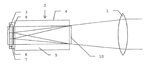
In order to improve target illumination, a light source (2) of an emitter,
which
has a laser diode (3) configured as an edge emitter with a wavelength of
1550nm, has
beam-forming optics (4) mounted downstream in relation thereto, which comprise
a
cylindrical lens (7) and a first deflection element (8) with three fields
having different
diffraction structures. Said deflection element deflects partial beams,
exiting from
successive segments of the emission edge, to three fields of a second
deflection
element (10) which are adjacent to each other and perpendicular to said
emission edge
and which also have different diffraction structures. Said second deflection
element
directs the partial beams to the aperture of a collimator (1), such that the
partial beams
substantially fill said aperture. The first deflection element (8) and a mount
(6) for the
cylindrical lens (7) are integral and, like the second deflection element
(10), are made
of plastic. Both parts are stuck on opposite faces of a block (5) made of
glass.


French Abstract

Afin d'améliorer l'éclairage d'une cible, une source lumineuse (2) d'un émetteur, comportant une diode laser (3) conçue sous la forme d'un émetteur par la tranche d'une longueur d'onde de 1 550 nm, présente un dispositif optique de mise en forme de faisceau (4), placé en aval et qui comprend une lentille cylindrique (7) ainsi qu'un premier élément de déviation (8), pourvu de trois champs présentant des structures de diffraction différentes. Cet élément de déviation diffracte des faisceaux partiels, émanant de sections successives de la tranche d'émission, sur trois champs d'un second élément de déviation (10) juxtaposés, perpendiculaires à cette tranche d'émission et présentant également des structures de diffraction différentes, lequel second élément de déviation oriente ces faisceaux partiels sur l'ouverture d'un collimateur (1), de sorte que ces faisceaux remplissent sensiblement ladite ouverture. Le premier élément de déviation (8) et un support (6) pour la lentille cylindrique (7) sont formés d'un seul tenant et fabriqués à partir d'une matière plastique, tout comme le second élément de déviation (10). Ces deux pièces sont collées sur des faces opposées d'un bloc (5) en verre.

Claims

Note: Claims are shown in the official language in which they were submitted.


7


1. Optical telemeter with at least one light source (2) for target
illumination and with a
collimator (1) collimating radiation emitted by the telemeter prior to target

illumination, the light source being arranged in front of the collimator (1)
and fitted with a
laser diode (3) formed as edge emitter, as well as with a receiver and a
control and
evaluating unit, characterized in that the light source (2) has beam forming
optics (4)
mounted downstream of the laser diode (3) and at least approximately
illuminating the
collimator (1), so designed that it offsets partial beams emitted from
successive segments
of the emission edge of laser diode (3) parallel to each other in such a way
that their
projections onto a plane overlap at least to a large extent, the plane being
rotated with
respect to the plane formed by the emission edge and a beam direction, the
beam forming
optics (4) comprising a first deflection element (8) based on diffraction or
refraction of
light, and a second deflection element (10) based on diffraction or refraction
of light,
each having an essentially plane surface with structuring, the structuring
being divided into
at least two fields (9a, 9b, 9c, 11a, 11b, 11c).


2. Optical telemeter according to claim 1, characterized in that laser diode
(3) emits
with a wavelength between 850 nm and 980 nm.


3. Optical telemeter according to claim 1, characterized in that laser diode
(3) emits
with a wavelength of approximately 1,550 nm.


4. Optical telemeter according to one of claims 1 to 3, characterized in that
the beam
forming optics (4) comprises a cylindrical lens (7) immediately following
after the laser
diode (3), the axis of this lens being parallel to the emission edge of the
laser diode (3).


5. Optical telemeter according to claim 4, characterized in that the diameter
of the
cylindrical lens (7) is at most 65 µm.


8


6. Optical telemeter according to claim 4 or 5, characterized in that the
distance
between the emission edge and the cylindrical lens (7) is at most 15 µm.


7. Optical telemeter according to one of claims 1 to 6, characterized in that
the first
deflection element (8) so deflects the partial beams in different ways in a
direction
transverse to the emission edge and also in a direction parallel to it that
they strike the
second deflection element (10) essentially side by side and the second
deflection element
(10) orients the partial beams in such a way as if they all issued from a line
in the focal
plane of collimator (1).


8. Optical telemeter according to claim 7, characterized in that the fields
(9a, 9b, 9c)
of the first deflection element (8) are oriented parallel to the emission edge
and contain
different diffraction structures, and that the number of fields (11a, 11b,
11c) of the second
deflection element (10) corresponds to the number of fields (9a, 9b, 9c) of
the first
deflection element (8), the fields (11a, 11b, 11c) of the second deflection
element (10)
containing different diffraction structures.


9. Optical telemeter according to one of claims 7 and 8, characterized in that
the first
deflection element (8) and the second deflection element (10) consist of
plastic.


10. Optical telemeter according to one of claims 7 to 9, characterized in that
the beam
forming optics (4) comprises a block (5) of transparent material with a first
front face to
which the first deflection element (8) is fastened and an opposite second
front face to
which the second deflection element (10) is fastened.


11. Optical telemeter according to claim 10, characterized in that the
cylindrical
lens (7) is tied to a mount (6) fastened to the first front face of block (5).


12. Optical telemeter according to claim 11, characterized in that the first
deflection
element (8) is integral with mount (6).


9
13. Optical telemeter according to claim 11 or 12, characterized in that the
laser
diode (3) is fastened by soldering to block (5).

14. Optical telemeter according to one of claims 4 to 10, characterized in
that the
cylindrical lens (7) is fastened to the laser diode (3) with cement.

15. Optical telemeter according to any one of claims 1 to 14, characterized in
that
the beam forming optics (4) is designed in such a way that the partial beams
are be
superimposed in the far field.

16. Optical telemeter according to any one of claims 1 to 15, characterized in
that the
beam forming optics (4) is designed in such a way that the partial beams in
the far field
are imaged onto a nearly square field.

Description

Note: Descriptions are shown in the official language in which they were submitted.


CA 02463679 2004-04-15

WO 03/033997 Al 1 PCT/EP01 12009
DESCRIPTION
OPTICAL TELEMETER

Technical field

The invention relates to an optical telemeter such as employed for instance in
the surveying
of plots of land and buildings.

Prior art

Optical telemeters of this kind have been known for some time already. The
laser diodes
used as light sources have the disadvantage, however, that the light beam
exiting at the
emission edge has a very long and narrow cross section. This leads to poor
target
illumination, since only part of the light beam strikes the target thus
detracting from the
range and from measuring accuracy. Moreover, reflection of parts of the beam
missing the
target at other objects, which for instance are more distant, may acutely
disturb the
measurements.

Description of the invention

The invention is based on the task to specify an optical telemeter of the
above kind
providing a better target illumination than known telemeters of this kind.

The advantages attained by the invention chiefly reside in a decisive
improvement of
range, i.e., the maximum distance that can be measured or, for a given range,
in an
increased measuring accuracy.

Brief description of the drawings
In the following, the invention is described in greater detail with the aid of
figures
representing merely one embodiment.


CA 02463679 2007-10-04

WO 03/033997 Al 2 PCT/EPO1 12009
Figure 1. schematically shows a lateral view of an emitter of a telemeter
according to the
invention,

Figure 2 schematically shows a top view of the emitter according to Figure 1
a,

Figure 3 shows a top view in beam direction of a first deflection element of
the emitter
according to Figures 1 a, b,

Figure 4 shows a top view counter to the beam direction of a second deflection
element of
the emitter according to Figures 1 a, b, and

Figure 5 shows the target illumination attained by the emitter according to
Figures 1 a, b.
Ways to practice the invention

An optical telemeter according to the invention comprises an emitter as well
as a receiver
that, in known manner, can for instance be built up with optics and avalanche
photodiodes,
and further comprises an electronic control and evaluating unit also of known
design
controlling the emission of light pulses by the emitter and evaluating the
output signal of
the receiver. The distance can be measured by transit-time determination or by
the phase-
matching technique.

The emitter has a collimator 1 and a light source 2 put in front of it which
is composed of a
laser diode 3 and beam forming optics 4. The laser diode 3 is an edge emitter
emitting
electromagnetic waves in the infrared, preferably at a wavelength between 850
nm and 980
nm or a wavelength k = 1,550 nm. The emission edge has a length between 30 m
and 800
m while its width is between 1 m and 3 m. The emission edge may be
interrupted in its
longitudinal direction. For instance, instead of one laser diode 3 a linear
array of laser
diodes having edge lengths of for instance 50 m and distances between
successive edges
of 100 m could be provided. The numerical aperture corresponding to the sine
of half the
angular aperture has a value of 0.1 parallel to the emission edge and of 0.6
to 0.7 transverse


CA 02463679 2004-04-15
WO 03/033997 Al 3 PCT/EP01 12009
to this edge. The product of these two quantities, known as space bandwith
product (SBP),
in a direction transverse to the emission edge approximately corresponds to
the wave-
length, and thus is practically monomodal (transverse mode of 0), i.e., it is
close to a
fundamental limiting value that cannot be exceeded, while parallell:o the
emission edge it
is larger than this limiting value by a factor of 10 to 100. Even in this
direction the SBP
cannot be altered by conventional refracting elements such as lenses, but with
the aid of
elements based on diffraction or refraction of light,. it can be lowered very
close to the
emission edge by rearrangement in a direction parallel to the emission edge
but instead be
enhanced in a direction transverse to this edge, and thus the light beam can
be more
strongly collimated.

This is the purpose of the beam forming optics 4 comprising a parallelepipedal
block 5
consisting of a transparent material, preferably glass, with a first front
face turned toward
the laser diode 3 and an opposite second front face turned toward the
collimator 1. The first
front face supports a mount 6 of plastic holding a cylindrical lens 7 at its
terminal zones.
The cylindrical lens 7 has a circular cross section, its diameter is about 60
m. It is oriented
parallel to the emission edge of laser diode 3 and spaced apart from 1:his
diode by about 10
m. The beam exiting from the emission edge which for laser diodes of the kind
employed
has a large transverse radiation angle of about 80 is made parallel by it.
The diameter of
the cylindrical lens and its distance from the emission edge may also be much
larger than
the given values, but for small values, particularly for values of at most 65
m and at most
15 m, respectively, the overlap of the fractions coherently radiated from
successive
regions of the edge is very small so that the losses caused by this overlap
are also kept low.

Downstream of the cylindrical lens 7 a first deflection element 8 is arranged
which is
integral with the mount 6 and has a structured surface that is essentially
plane and parallel
to the first front face of block 5. Parallel to the emission edge it is
divided into three
successive fields 9a, b, c having different stepped diffraction structures.
The second,
opposite front face of block 5 supports a second deflection element 10
consisting of plastic
and comprising a structured surface essentially plane and parallel to the
second front face
that is divided into three successive fields 11 a, b, c transverse to the
emission edge also
having different stepped diffraction structures.


CA 02463679 2004-04-15
WO 031033997 Al 4 PCT/EP01 12009
The upper field 9a of the first deflection element 8 has a structure such that
it deflects the
partial beam exiting from an upper segment of the emission edge anci striking
it to the left-
hand field 11 a (looking in beam direction) of the second deflection element
10 where the
beam is insignificantly deflected so that it will strike the collimator 1 and
approximately
fill the left-hand third of the collimator's aperture. In exactly
corresponding manner, the
lower field 9c of the first deflection element 8 deflects the partial beam
exiting from a
lower segment of the emission edge and striking it, to the right-hand field 1
lc (looking in
beam direction) of the second deflection element 10, where this beam, too, is
deflected
precisely in the corresponding way and then fills approximately the i-ight-
hand third of the
aperture of collimator 1. The central third of the collimator is filled by the
partial beam
exiting from a slightly shorter central segment of the emission edge and
passing without
deflection through the unstructured central fields 9b and 11b of the first
deflection element
8 and second deflection element 10, respectively.
Thus, the three partial beams are so deflected in different ways by the first
deflection
element 8 that they strike the second deflection element 10 side by side (when
looking in a
direction transverse to the emission edge), hence their projections onto a
plane formed,
purely as an example here, by the directions of the emission edge and of the
beam
essentially coincide. However, a deflection can also occur in such a way that
the projection
occurs onto a plane which for instance is rotated relative to the plane formed
by the
directions of the emission edge and of the beam. The essential point is that
of avoiding a
crossing of the partial beams. A deflection according to the invention can be
functionally
integrated into the deflection element 8 by suitable design of this element or
by additional
elements, which may where appropriate even be applied to the deflection
element.

In the second deflection element 10 the partial beams are then so deflected in
different
ways that they strike the collimator 1 as if they all came from a line
parallel to, or rotated
relative to, the emission edge in the focal plane of collimator 1 or, stated
differently, in
such a way that their back extrapolation will lead to such a line, and that
each partial beam
fills approximately one third of the aperture of collimator 1. The three
successive segments
of the emission edge are imaged onto a nearly square field, and indeed in such
a way that


CA 02463679 2004-04-15
WO 03/033997 Al 5 PCT/EP01 12009
they are superimposed in the far field (Figure 5). This secures an excellent
target
illumination.

At wavelengths between 850 nm and 950 nm the beam can be collimated very
strongly,
allowing a range scan with high lateral resolution. Wavelengths around 1,550
nm are also
very advantageous, since then the upper limit of the admissible single-pulse
energy which
is defined in terms of safety to the eyes has a value of about 8 mJ and thus
is higher by a
factor of about 16,000 than at wavelengths between 630 and 980 nm. By
employing this
factor at least in part, which becomes possible because of better beam
concentration
according to the invention, one can very substantially increase the range or,
for a given
range, raise the sensitivity.

The mount 6 and the first deflection element 8 that is integral with it., as
well as the second
deflection element 10, each are produced by one of the replication techniques
as described
in M. T. Gale, `Replication', in H. P. Herzig (editor), `Micro-Optics', Taylor
& Francis
1997, pp. 153-177, for instance by etching of a cylinder or piston of quartz
and by hot
embossing, injection molding, or casting followed by UV curing, and are then
bonded to
block 5. The definition of the diffraction structures can be performed with
known computer
programs. The replication technique allows large numbers of parts to be
fabricated at
favorable cost. Since the mount 6 is also made by this technique, a very
precise positioning
of cylindrical lens 7 is possible. The tolerated variation of distance between
the lens and
the first deflection element 8 is a few micrometers. Using soldering and
active adjustment
as described in DE-A-197 51 352, the laser diode 3 can then be bonded in such
a way to
the beam forming optics 4 that the tolerated variation of mounting between it
and the
cylindrical lens 7 is about 0.5 m.

Various modifications of the embodiment described are possible. Thus, the
cylindrical lens
may be fastened with cement directly to the laser diode. The first de;flection
element and
the second deflection element may also consist of glass, and for instance be
made by an
etching process. They may also be etched directly into the block separating
them. The
number of fields in the deflection elements may be two, four or more, instead
of three. The
beam forming optics may also consist of refracting elements, for instance
prisms and


CA 02463679 2004-04-15
WO 03/033997 Al 6 PCT/EPO1 12009
plates. Finally, laser diodes having wavelengths particularly between 600 nm
and 1,000
nm, and more particularly between 630 nm and 980 nm which are outside the
regions
indicated above can be employed.

List of reference symbols
1 Collimator
2 Light source
3 Laser diode
4 Beam forming optics
5 Block
6 Mount
7 Cylindrical lens
8 first deflection element
9a,b,c Fields
10 second deflection element
11 a,b,c Fields

Representative Drawing
A single figure which represents the drawing illustrating the invention.
Administrative Status

For a clearer understanding of the status of the application/patent presented on this page, the site Disclaimer , as well as the definitions for Patent , Administrative Status , Maintenance Fee  and Payment History  should be consulted.

Administrative Status

Title Date
Forecasted Issue Date 2009-08-04
(86) PCT Filing Date 2001-10-17
(87) PCT Publication Date 2003-04-24
(85) National Entry 2004-04-15
Examination Requested 2006-09-13
(45) Issued 2009-08-04
Expired 2021-10-18

Abandonment History

There is no abandonment history.

Payment History

Fee Type Anniversary Year Due Date Amount Paid Paid Date
Registration of a document - section 124 $100.00 2004-04-15
Application Fee $400.00 2004-04-15
Maintenance Fee - Application - New Act 2 2003-10-17 $100.00 2004-04-15
Maintenance Fee - Application - New Act 3 2004-10-18 $100.00 2004-10-12
Maintenance Fee - Application - New Act 4 2005-10-17 $100.00 2005-09-23
Request for Examination $800.00 2006-09-13
Maintenance Fee - Application - New Act 5 2006-10-17 $200.00 2006-09-20
Maintenance Fee - Application - New Act 6 2007-10-17 $200.00 2007-09-24
Maintenance Fee - Application - New Act 7 2008-10-17 $200.00 2008-09-23
Final Fee $300.00 2009-05-21
Maintenance Fee - Patent - New Act 8 2009-10-19 $200.00 2009-10-02
Maintenance Fee - Patent - New Act 9 2010-10-18 $200.00 2010-09-23
Maintenance Fee - Patent - New Act 10 2011-10-17 $250.00 2011-10-06
Maintenance Fee - Patent - New Act 11 2012-10-17 $250.00 2012-10-04
Maintenance Fee - Patent - New Act 12 2013-10-17 $250.00 2013-10-07
Maintenance Fee - Patent - New Act 13 2014-10-17 $250.00 2014-10-06
Maintenance Fee - Patent - New Act 14 2015-10-19 $250.00 2015-10-05
Maintenance Fee - Patent - New Act 15 2016-10-17 $450.00 2016-10-03
Maintenance Fee - Patent - New Act 16 2017-10-17 $450.00 2017-10-09
Maintenance Fee - Patent - New Act 17 2018-10-17 $450.00 2018-10-08
Maintenance Fee - Patent - New Act 18 2019-10-17 $450.00 2019-10-07
Maintenance Fee - Patent - New Act 19 2020-10-19 $450.00 2020-10-05
Owners on Record

Note: Records showing the ownership history in alphabetical order.

Current Owners on Record
LEICA GEOSYSTEMS AG
Past Owners on Record
GAECHTER, BERNHARD
SCHILLING, ANDREAS
STAUFFER, LAURENT
VOKINGER, URS
Past Owners that do not appear in the "Owners on Record" listing will appear in other documentation within the application.
Documents

To view selected files, please enter reCAPTCHA code :


To view images, click a link in the Document Description column. To download the documents, select one or more checkboxes in the first column and then click the "Download Selected in PDF format (Zip Archive)" or the "Download Selected as Single PDF" button.

List of published and non-published patent-specific documents on the CPD .

If you have any difficulty accessing content, you can call the Client Service Centre at 1-866-997-1936 or send them an e-mail at CIPO Client Service Centre.


Document
Description 
Date
(yyyy-mm-dd) 
Number of pages   Size of Image (KB) 
Cover Page 2009-07-09 1 44
Abstract 2004-04-15 1 26
Claims 2004-04-15 3 112
Drawings 2004-04-15 1 28
Description 2004-04-15 6 286
Representative Drawing 2004-04-15 1 6
Cover Page 2004-06-14 1 43
Representative Drawing 2009-07-09 1 6
Description 2007-10-04 6 285
Claims 2007-10-04 3 110
Drawings 2007-10-04 1 25
Claims 2008-10-21 3 109
Abstract 2004-04-15 1 26
Assignment 2004-07-28 4 119
PCT 2004-04-15 14 666
Assignment 2004-04-15 3 88
PCT 2004-04-15 10 439
Correspondence 2004-06-09 1 25
Prosecution-Amendment 2006-09-13 1 40
Fees 2004-10-12 1 32
Prosecution-Amendment 2007-05-22 3 90
Prosecution-Amendment 2007-03-20 1 35
Prosecution-Amendment 2007-10-04 7 249
Prosecution-Amendment 2008-05-06 1 33
Prosecution-Amendment 2008-10-21 4 116
Correspondence 2009-05-21 2 50