Note: Descriptions are shown in the official language in which they were submitted.
CA 02463768 2004-04-14
WO 03/040671 PCT/US02/33585
1
ACCURACY CALIBRATION OF BIREFRINGENCE MEASUREMENT
SYSTEMS
This application claims the benefit of the filing date of US Provisional
Patent
Application No. 60/329,680, hereby incorporated by reference.
Technical Field
This application generally relates to systems that precisely measure
birefringence properties of optical elements, and particularly to the use of a
Soleil-
Babinet compensator for calibrating such systems.
Background
Many important optical materials exhibit birefringence. Birefringence means
that different linear polarizations of light travel at different speeds
through the
material. These different polarizations are most often considered as two
components
of the polarized light, one being orthogonal to the other.
Birefringence is an intrinsic property of many optical materials, and may be
induced by external forces. Retardation or retardance represents the
integrated effect
of birefringence acting along the path of a light beam traversing the sample.
If the
incident light beam is linearly polarized, two orthogonal components of the
polarized
light will exit the sample with a phase difference, called the retardance. The
fundamental unit of retardance is length, such as nanometers (nm). It is
frequently
convenient, however, to express retardance in units of phase angle (waves,
radians, or
degrees), which is proportional to the retardance (nm) divided by the
wavelength of
the light (nm). An "average" birefringence for a sample is sometimes computed
by
dividing the measured retardation magnitude by the thickness of the sample.
Oftentimes, the term "birefringence" is interchangeably used with and carries
the same meaning as the term "retardance." Thus, unless stated otherwise,
those
terms are also interchangeably used below.
The two orthogonal polarization components described above are parallel to
two orthogonal axes, which are determined by the sample and are respectively
called
the "fast axis" and the "slow axis." The fast axis is the axis of the material
that aligns
with the faster moving component of the polarized light through the sample.
Therefore, a complete description of the retardance of a sample along a given
optical
CA 02463768 2004-04-14
WO 03/040671 PCT/US02/33585
path requires specifying both the magnitude of the retardance and its relative
angular
orientation of the fast (or slow) axis of the sample.
The need for precise measurement of birefringence properties has become
increasingly important in a number of technical applications. For instance, it
is
impoutant to specify linear birefringence (hence, the attendant induced
retardance) in
optical elements that are used in high-precision instruments employed in
semiconductor and other industries.
Moreover, the optical lithography industry is transitioning to the use of very
short exposure wavelengths for the purpose of further reducing line weights
(conductors, etc.) in integrated circuits, thereby to enhance performance of
those
circuits. In this regard, the next generation of optical lithography tools
will use laser
light having a wavelength of about 157 nanometers, which wavelength is often
referred to as deep ultraviolet or DUV.
It is important to precisely determine the retardance properties of optical
elements or components that are used in systems, such as lithography tools,
that
employ DUV. Such a component may be, for example, a calcium fluoride (CaF2)
lens
of a scanner or stepper. Since the retardance of such a component is a
characteristic
of both the component material as well as the wavelength of light penetrating
the
material, a system for measuring retardance properties must operate with a DUV
light
source and associated components for detecting and processing the associated
light
signals.
The magnitude of the measured retardance of an optical element is a function
of the thickness of the element, the thickness being measured in the direction
that the
light propagates through the sample. For example, a CaF2 optical element will
have
an intrinsic birefringence of about 11 nm for every centimeter (cm) of
thickness.
Consequently, for example, a 10 cm-thiclc CaF2 element will have a relatively
high
birefringence level of about 110 nanometers, which is about three-quarters of
a 157
nm DUV wavelength.
Systems for measuring birefringence of a sample have been developed and use
an optical setup (arrangement of light source, optical elements, detectors
etc.) that
includes polarization modulators. An example of such a system is described in
US
CA 02463768 2004-04-14
WO 03/040671 PCT/US02/33585
3
Patent No. 6,473,179 and includes a photoelastic modulator (PEM) for
modulating
polarized light that is then directed through a sample. The beam propagating
from the
sample is separated into two parts. These separate beam parts are then
analyzed at
different polarization directions, detected, and processed as distinct
channels. The
detection mechanisms associated with each channel detect the light intensity
corresponding to each of the two parts of the beam. This information is
employed in
an algorithm for calculating a precise, unambiguous measure of the.retardance
induced by the sample as well as the angular orientation of birefringence
relative to
the fast axis of the sample.
Birefringence measurement systems such as the exemplary one just mentioned
may be constructed to be self-calibrating. However, such a system requires
extremely
accurate settings to report accurate results. It is therefore useful to have a
reliable way
of calibrating such systems by using an external optical element.
Summary of the Invention
The present invention is directed to the use of a Soleil-Babinet compensator
as
an external optical element for calibrating birefringence measurement systems.
A
Soleil-Babinet compensator is an instrument that includes movable optical
elements
for inducing a lcnown, selected retardance to a light beam that propagates
through it.
Highly precise and repeatable calibration is accomplished by the method
described
here because, among other things, the inventive method accounts for variations
of
retardance across the surface of the Soleil-Babinet compensator.
The calibration technique described here may be employed in birefringence
measurement systems that have a variety of optical setups for measuring a
range of
retardation levels and at various frequencies of light sources. For example,
the
present invention is adaptable to systems that precisely measure birefringence
properties of optical elements such as those elements that are used in DUV
applications as mentioned above.
The approach to calibration in accordance with the present invention can be
selectively varied somewhat in complexity to allow for the use of versions of
the
CA 02463768 2004-04-14
WO 03/040671 PCT/US02/33585
4
method to match the desired accuracy of the system with which the calibration
method is employed. .
Other advantages and features of the present invention will become clear upon
study of the following portion of this specification and drawings.
Brief Description of Drawings
Fig. 1 is a diagram of a birefringence measurement system to which one
embodiment of the present invention may be adapted.
Fig. 2 is a block diagram of the signal processing components of the system of
Fig. 1.
Fig. 3 is a perspective view of detection and beam-splitting components of the
system of Fig. 1.
Fig. 4 is a cross-sectional view of one of the detector assemblies of the
system
of Fig. 1.
Fig. 5 is a perspective view of the primary components of a photoelastic
modulator that is incorporated in the system of Fig. 1.
Fig. 6 is a drawing depicting a graphical display provided by the system of
Fig. 1.
Fig. 7 is a diagram of another birefringence measurement system to which one
embodiment of the present invention may be adapted.
Fig. 8 is a block diagram of the signal processing components of the system
depicted in Fig. 7.
Fig. 9 is a diagram of another birefringence measurement system to which one
embodiment of the present invention may be adapted.
Fig. 10 is a blocle diagram of the signal processing components of the system
depicted in Fig. 9.
Best Modes for Carrying Out the Invention
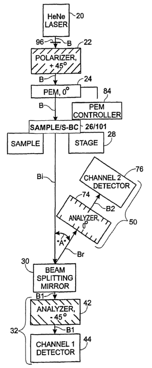
The diagram of Fig. 1 depicts the primary optical components of a system that
can be calibrated in accordance with the present invention. The components
include a
HeNe laser as a light source 20 that has a wavelength of 632.8 nanometers
(nm). The
CA 02463768 2004-04-14
WO 03/040671 PCT/US02/33585
S
beam "B" emanates from the source along an optical path and has a cross
sectional
area or "spot size" of approximately 1 millimeter (rnm).
The source light beam "B" is directed to be incident on a polarizes 22 that is
oriented with its polarization direction at +45° relative to a baseline
axis. A high-
s extinction polarizes, such as a Glan-Thompson calcite polarizes, is
preferred. It is also
preferred that the polarizes 22 be secured in a precision, graduated rotator.
The polarized light from the polarizes 22 is incident on the optical element
25
of a photoelastic modulator 24 (Figs. 1 and 5). In a preferred embodiment, the
photoelastic modulator (hereafter referred to as a "PEM") is one manufactured
by
Hinds Instruments, Inc., of Hillsboro, Oregon, as a low birefringence version
of
Model PEM-90 I/FS50. It is noteworthy here that although a PEM is preferred,
one
could substitute other mechanisms for modulating the polarization of the
source light.
The PEM has its birefringent axis oriented at 0° and is controlled
by a
controller 84 that impacts an oscillating birefringence to the optical element
25,
preferably at a nominal frequency of 50 lcliz. In this regard, the controller
84 drives
two quartz transducers 29 between which the optical element 25 is bonded with
an
adhesive.
The oscillating birefringence of the PEM introduces a time-varying phase
difference between the orthogonal components of the polarized light that
propagates
through the PEM. At any instant in time, the phase difference is the
retardation
introduced by the PEM. The retardation is measurable in units of length, such
as
nanometers. The PEM is adjustable to allow one to vary the amplitude of the
retardation introduced by the PEM. In the case at hand, the retardation
amplitude is
selected to be 0.383 waves (242.4 nm).
The beam of light propagating from the PEM is directed through the
transparent sample 26. The sample is supported in the path of the beam by a
sample
stage 28 that is controllable for moving the sample in a translational sense
along
orthogonal (X and Y) axes. The stage may be any one of a number of
conventional
designs such as manufactured by THK Co. Ltd., of Tokyo, Japan as model KR2602
A-250. As will become clear, the motion controllers of the sample stage 28 are
driven
CA 02463768 2004-04-14
WO 03/040671 PCT/US02/33585
6
to enable scanning the sample 26 with the beam to arrive at a plurality of
retardance
and orientation measurements across the area of the sample.
The sample 26 will induce retardance into the beam that passes through it.
The system depicted Figs. 1 and 2 determines this retardance value, as
explained more
below. The system is especially adapted to determine low levels of retardance.
Low
retardance levels are determined with a sensitivity of less than ~ 0.01 nm.
In order to obtain an unambiguous measure of the sample-induced retardance,
the beam "Bi" that passes out of the sample is separated into two parts having
different polarization directions and thereby defining two channels of
information for
subsequent processing.
A beam-splitting mirror 30 for separating the beam "Bi" is located in the path
of that beam (hereafter referred to as the incidence path). Part "B 1" of the
beam "Bi"
passes completely through the beam-splitting mirror 30 and enters a detector
assembly 32 for detection.
Fig. 3 depicts a mechanism for supporting the beam-splitting mirror 30. In
particular, the mirror 30 is seated in the central aperture of a housing 31
that is rigidly
supported by an arm 33 to a stationary veutical post 36. The post 36 is
employed for
supporting all of the optical components of the system so that the paths of
the light are
generally vertical.
The diameter of the mirror 30 is slightly less than the diameter of the
housing
aperture. The aperture is threaded except for an annular shoulder that
projects into the
lowermost end of the aperture to support the periphery of the flat, round
mirror 30. A
retainer ring 40 is threaded into the aperture to keep the mirror in place in
the housing
31 against the shoulder.
The mirror 30 is selected and mounted so that substantially no stress-induced
birefringence is introduced into the mirror. In this regard, the mirror is
preferably
made of Schott Glass type SF-57 glass. This glass has an extremely low (near
zero)
stress-optic coefficient. The retainer ring 40 is carefully placed to secure
the mirror
without stressing the glass. Alternatively, flexible adhesive may be employed
to
fasten the mirror. No setscrews or other stress-inducing mechanisms are
employed in
CA 02463768 2004-04-14
WO 03/040671 PCT/US02/33585
7
mounting the mirror. Other mechanisms (such as a flipper mirror arrangement)
for
separating the beam "Bi" into two parts can be used.
The part of the beam "B 1" that passes through the mirror 30 enters the
detector assembly 32 (Fig. 1), which includes a compact, Glan-Taylor type
analyzer
42 that is arranged such that its polarization direction is at -45°
from the baseline axis.
From the analyzer 42, the beam "B1" enters a detector 44, the particulars of
which are
described more below.
The reflective surface 35 of the beam-splitting mirror 30 (Fig. 3) faces
upwardly, toward the sample 26. The mirror is mounted so that the incidence
path
(that is, the optical path of the beam "Bi" propagating from the sample 26) is
nearly
normal to the reflective surface 35. This orientation substantially eliminates
retardance that would otherwise be introduced by an optical component that is
called
on to redirect the path of the beam by more than a few degrees.
Fig. 1 shows as "A" the angle made between the beam "Bi" traveling along
the incidence path and the beam part "Br" that is reflected from the mirror
30. Angle
"A" is shown greatly enlarged for illustrative purposes. This angle is
generally about
5°.
The reflected part of the light beam "Br" is incident upon another detector
assembly 50. That assembly 50 is mounted to the post 36 (Fig. 3) and
configured in a
way that permits the assembly to be adjacent to the incident beam "Bi" and
located to
receive the reflected beam "Br." More particularly, the assembly 50 includes a
base
plate 52 that is held to the post 36 by an arm 54. As seen best in Fig. 4, the
base plate
includes an inner ring 57 that is rotatably mounted to the base plate and has
a large
central aperture 56 that is countersunk to define in the bottom of the plate
52 an
annular shoulder 58.
The detector components are compactly integrated and contained in a housing
60 that has a flat front side 62. The remainder of the side of the housing is
curved to
conform to the curvature of the central aperture 56 of the base plate 52.
Moreover,
this portion of the housing 60 includes a stepped part 64 that permits the
curved side
of the housing to fit against the base plate 52 and be immovably fastened
thereto.
CA 02463768 2004-04-14
WO 03/040671 PCT/US02/33585
g
A sub-housing 70 is fastened inside of the detector components housing 60
against the flat side 62. The sub-housing 70 is a generally cylindrical member
having
an aperture 72 formed in the bottom. Just above the aperture 72 resides a
compact,
Glan-Taylor type analyzer 74 that is arranged so that its polarization
direction is 0°,
parallel with that of the PEM 24.
Staclced above the analyzer 74 is a narrow-band interference filter 77 that
permits passage of the polarized laser light but blocks unwanted room light
from
reaching a detector 76. The detector is preferably a photodiode that is
stacked above
the filter. The photodiode detector 76 is the preferred detection mechanism
and
produces as output a current signal representative of the time varying
intensity of the
received laser light. With respect to this assembly 50, the laser light is
that of the
beam "B2," which is the reflected part "Br" of the beam that propagated
through the
sample 26.
The photodiode output is delivered to a preamplifier carried on an associated
printed circuit board 78 that is mounted in the housing 60. The preamplifier
75 (Fig.
2) provides output to a phase sensitive device (preferably a lock-in amplifier
80) in
the form of a low-impedance intensity signal VAC, and a IBC intensity signal
VDC,
which represents the time average of the detector signal.
The other detector assembly 32 (Fig. 3) to which is directed the non-reflected
part "B 1" of the beam "Bi" is, except in two respects, the same construction
as the
just described assembly 50. As shown in Fig. 3, the detector assembly 32 is
mounted
to the post 36 in an orientation that is generally inverted relative to that
of the other
detector assembly 50. Moreover, the analyzer 42 of that assembly 32 is
arranged so
that its polarization direction is oblique to the polarization direction of
the analyzer 74
in the other detector assembly 50. Specifically, the analyzer 42 is positioned
with its
polarization direction at -45°. The preferred analyzer position is
established by
rotating the detector assembly via the inner ring 57 discussed above.
The photodiode of detector assembly 32 produces as output a current signal
representative of the time varying intensity of the received laser light. With
respect to
this assembly 32, the laser light is that of the beam "B1," which is the non-
reflected
part of the beam "Bi" that propagated through the sample 26.
CA 02463768 2004-04-14
WO 03/040671 PCT/US02/33585
9
The photodiode output of the detector assembly 32 is delivered to a
preamplifier 79, which provides its output to the lock-in amplifier 80 (Fig.
2) in the
form of a low-impedance intensity signal VAC, and a DC intensity signal VDC,
which represents the time average of the detector signal.
In summary, the lock-in amplifier 80 is provided with two channels of input:
channel 1 corresponding to the output of detector assembly 32, and channel 2
corresponding to the output of detector assembly 50. The intensity information
received by the lock-in amplifier on channel 1-because of the arrangement of
the -
45° analyzer 42- relates to the 0° or 90° component of
the retardance induced by the
sample 26. The intensity information received on channel 2 of the lock-in
amplifier
80 -as a result of the arrangement of the 0° analyzer 74- relates to
the 45° or -45°
component of the retardance induced by the sample. As explained below, this
information is combined in an algorithm that yields an unambiguous
determination of
the magnitude of the overall retardance induced in the sample (or a location
on the
sample) as well as the orientation of the fast axis of the sample (or a
location on the
sample).
The Ioclc-in amplifier 80 may be one such as manufactured by EG&G Tnc., of
Wellesley, Massachusetts, as model number 7265. The lock-in amplifier takes as
its
reference signal 82 the oscillation frequency applied by the PEM controller 84
to the
transducers 29 that drive the optical element 25 of the PEM 24. The loclc-in
amplifier
80 communicates with a digital computer 90 via an RS232 serial interface.
For a particular retardance measurement, such as one taken during the
scanning of several locations on a sample, the computer 90 obtains the values
of
channel 1. The computer next obtains the values of channel 2. The intensity
signals
on the detectors in channels 1 and 2 are derived as follows:
I~,n =1+cos(4p)sin2 ~ cos0-cos' ~ cosh+cos(2p)sin~sin~
eqn. (1)
I~~t2 =1 + sin(4p) sine ~ cos0 + sin(2p) sin~sin0
CA 02463768 2004-04-14
WO 03/040671 PCT/US02/33585
where 0 is the PEM's time varying phase retardation; 8 is the magnitude of the
sample's retardance; and p is the azimuth of the fast axis of the sample's
retardance.
The Mueller matrix for a linearly birefringent sample (b, p) used in the
derivation has
the following form:
1 a a a
s~ s~ . . s~
I cos (~'P~'s~n - + GoS - s~ (4'P~'s~i - - stn (~'P)'s~ (~ ~
sip (4'P~'sin ~ - cos (4'P~'s~i ~ + cos ~ cos (~'P~'sin (& ~
sin (2'P) 'sin (& ) - (~o~ (~'P~'s~ (& ) ~ ros (~ ~
5
In equations (1), sin0 (4= DOsinc~t, where cu is the PEM's modulating
frequency; ~0 is the maximum peak retardance of the PEM) can be expanded with
the
Bessel functions of the first bind:
sin ~ = sin(~o sin(~t)) = ~ 2J2k+~ (do ) sin((2k + 1)cot) eqn. (2)
2k+t
10 where k is either "0" or a positive integer; and J2k+1 is the (2k+I)th
order of the
Bessel function. Similarly, cosh can be expanded with the even harmonics of
the
Bessel functions:
cosh = cos(Do sin(ecx-)) = J~ (Do ) +~2J2k (Do ) cos(~k)~cx~) eqn. (3)
2k
where Jo is the Oa' order of the Bessel function, and J2k is the (21c)th order
of
the Bessel function.
CA 02463768 2004-04-14
WO 03/040671 PCT/US02/33585
11
As seen from eqns. 1-3, it is preferable to determine the magnitude and
angular orientation of retardance using the signal at the PEM's first
harmonic. The
useful signal for measuring linear birefringence at the PEM's 2nd harmonic is
modified by sin2.(8/2), a value that is much smaller than sin8. The 1F
electronic
signal on the detectors can be expressed in equation (4):
1 cFzl,lF = sin ~ cos( 2 p)2J1 (~ o ) sin( wt)
I ch 2 ,1 F = sin ~ sin( 2 p ) 2 J 1 ( 0 0 ) sin( ~t ) eqn. (4)
As noted, the 1F signal is determined using the lock-in amplifier 80 that is
referenced at the PEM's first harmonic. The lock-in amplifier will exclude the
contributions from all harmonics other than 1F. The output from the loclc-in
amplifier
80 for the two channels is:
I~hl(1F)= sin ~cos( 2p)2J1(~o)~
I (1 F ) = sin ~ sin( 2 p ) 2 J 1 ( 0 0 ) ~ eqn. (5)
~n a
The value ~2 results from the fact that the lock-in amplifier measures the
r.m.s. of the signal, instead of the amplitude.
All terms appearing at a frequency other than the PEM's first harmonic are
neglected in obtaining equations (5). The validity of equations (5) for
obtaining the
1F VAC signal is further ensured from the approximation that sin'(~/2) ~ 0
when b is
small. This applies for low-level retardance of, for example, less than 20 nm.
In order to eliminate the effect for intensity fluctuation of the light
source, or
variations in transmission due to absorption, reflection losses, or
scattering, the ratio
of the 1F VAC signal to the VDC signal is used. (Alternatively, similar
techniques can
be employed, such as dynamically normalizing the DC signal to unity.)
Exclusion of
the cos0 terms in equation (1) can severely affect the VDC signal in channel 1
even
though it has a minimal effect on the determination of the 1F VAC signal using
a high
quality lock-in amplifier. The term cos2(8/2)cos0 in equation (1) is
approximately
equal to cosh for small b. As seen from equation (3), cos0 depends on Jo(Do),
which
is a "DC" term. Consequently, this DC term should be corrected as in equations
(6):
CA 02463768 2004-04-14
WO 03/040671 PCT/US02/33585
12
I~n~ClF) 1- Jo(Do) I = R~n~ = sin Scos( 2p)
I~C . 2J1(L~o) .
I (1 F ~ 1 1 eqn. (6)
~~' z = R = sin ~ sin( 2 p )
1~~ . 2J1(~o) ~ ~ ~nz
where R~jtl and R~~12 are experimentally determined quantities from the two
channels.
To correct the "DC" term caused by the cos0 term in channel 1, one properly
sets the PEM retardation so that Jo(~o) = 0 (when Do = 2.405 radians, or 0.383
waves).
At this PEM setting, the efficiency of the PEM for generating the 1F signal is
about
90°70 of its maximum.
Finally, the magnitude and angular orientation of the linear birefringence is
expressed in equations (7):
p =1 tari 1 R~hz oY p =1 ctg i R~hi
~ R~hi ~ R~ha eqn. (7)
_ 2
= Slll 1 (Rch1 )2 + (Rch2 )
The retardation b is represented in radians. It can be converted to degrees,
number of waves and nanometers "nm" at the wavelength of measurement (e.g.,
632.8
nm as used here). Thus, the above retardation is converted to nanometers "nm"
by
multiplying that amount by the wavelength (in nm) divided by 2~.
These equations (7) are compiled in a program running on the computer 90
and used to determine the magnitude and orientation of the retardance at any
selected
point on the sample.
The birefringence measurement system described here employs a PEM 24
(Fig. 5) that is specially configured to eliminate residual birefringence that
may result
from supporting the optical element 25 of the PEM in the housing 27 (shown in
dashed lines of Fig. 5). The bar-shaped optical element is bonded at each end
to a
transducer 29. Each transducer 29 is mounted to the PEM housing 27, as by
supports
23, so that the optical element is essentially suspended, thus free from any
residual
CA 02463768 2004-04-14
WO 03/040671 PCT/US02/33585
13
birefringence that may be attributable to directly mounting the oscillating
optical
element 25 to the PEM housing 27.
The results of equations 8 are corrected to account for any remaining residual
birefringence in the system, which residual may be referred to as the system
offset. In
practice, residual birefringence in the optical element of the photoelastic
modulator
and in the beam-splitting mirror substrate can induce errors in the resulting
measurements. Any such errors can be measured by first operating the system
with
no sample in place. A correction for the errors is made by subtracting the
error values
for each channel.
The system offset is obtained by mal~ing a measurement without a sample in
place. The results from both channels 1 and 2 are the system offsets at
0° and 45°
respectively:
0
o. I~m(1F ) _ sin ~S°(p = 0)
~n i = o
2 J 1 ( 0 0 ) I ~rm eqn. (8)
0
R h' 2 J ~(~(1)1~ - sin & ° (p = 4 )
i o d~ z
where the superscript "0" indicates the absence of a sample. The equation
bearing the term p = 0 corresponds to channel 1 (the -45° analyzer 42).
The equation
bearing the temp p = ~/4 corresponds to channel 2 (the 0° analyzer 74).
The system
offsets are corrected for both channels when a sample is measured. The system
offsets for channels 1 and 2 are constants (within the measurement error) at a
fixed
instrumental configuration. Barring any changes in the components of the
system, or
in ambient pressure or temperature, the system's offsets should remain the
same.
In principle, this system is self-calibrating with ideal settings for all
components in the system. It is, however, prudent to compare the system
measurement of a sample with the measurement obtained using other methods as
explained next.
In accordance with the present invention a conventional Soleil-Babinet
compensator is used as an external optical element in one method for
calibrating the
accuracy of a birefringence measurement system such as the one just described
with
CA 02463768 2004-04-14
WO 03/040671 PCT/US02/33585
14
respect to Figs. 1 - 5. During the calibration process, the Soleil-Babinet
compensator
101 (Fig. 1) is substituted for the sample 26, as explained more below.
A suitable Soleil-Babinet compensator 101 may be one as manufactured by
Special Optics, of Wharton, New Jersey. It is composed of three single-crystal
quartz
(or magnesium fluoride for use with the DUV birefringence measurement systems
described below) optical elements: one fixed wedge, one translational wedge,
and one
rectangular prism. The two quartz (or magnesium fluoride) wedges have their
principal optical axes parallel to each other while the quartz (or magnesium
fluoride)
prism has its principal optical axis perpendicular to that of the wedge
assembly. The
mechanical translation of one of the quartz (or magnesium fluoride) wedges is
by a
micrometer, thereby providing the selectable variation of retardation induced
by the
compensator. Such compensators are generically known as mechanically variable
retarders.
The Soleil-Babinet compensator is mounted on a ball bearing indexing head
which has a fixed outer circumference graduated 0°, 180°,
+45°, +90°, +135°, -45°, -
90° and -135°. The inner circumference carries the optical
elements and is rotatable
through 360° and has indicator marks at one-degree increments. A
knurled locking
screw in the outer circumference is used to fix the rotational position.
Precise and repeatable calibration is accomplished by the method described
hereafter because, among other things, the method accounts for variations of
retardance that may occur across the surface of the Soleil-Babinet
compensator.
In accordance with one approach to the present invention, the birefringence
measurement system accuracy calibration method begins by locating the Soleil-
Babinet compensator 101 in the position normally assumed by the sample 26. The
compensator 101 is then oriented at exactly 0° ("0°" is defined
by the PEM's optical
axis in the birefringence measurement system). This orientation is
accomplished by
minimizing the PEM's first harmonic signal at the channel 2 detector 76 while
rotating the Soleil-Babinet compensator. As previously described, the 1F
signal at
channel 2 of the birefringence system is nulled when the sample is oriented at
"0°"
Preferably, a fairly large retardation level should be selected on the Soleil-
Babinet compensator during this orientation or aligning step so that one
obtains an
CA 02463768 2004-04-14
WO 03/040671 PCT/US02/33585
Z$
angular accuracy of about 0.05 degrees. In this embodiment, for example, a
retardation level of about 100 nm should be set at the Soleil-Babinet
compensator.
Put another way, at such a retardation level a change in the 1F signal at
channel 2 of
about 0.1 mV is easily observable, and corresponds to a less than 5 miliarc
angle
change of the Soleil-Babinet compensator. The maximum 1F signal when the
Soleil-
Babinet compensator is oriented at 45° is usually about 400 mV.
The modulation of the light beam is then halted, preferably by removing the
PEM 24 from the path of the beam "B." This approach eliminates concerns about
any
residual birefringence in the PEM affecting the accuracy of the calibration
process.
As an acceptable alternative, however, the PEM 24 may merely be turned off and
remain in the path of the beam. This alternative is acceptable when, as here,
the PEM
has a residual birefringence of less than 0.2 nm. Also, depending on the
configuration
of the optical setup, this alternative may make it easier to maintain the
position of the
beam on a single location of the Soleil-Babinet compensator aperture surface,
which
is required for greatest accuracy.
The beam-splitting mirror 30 is removed from the optical path of the beam B.
It will be appreciated that, as respects channel 1, the resulting setup thus
places the
Soleil-Babinet compensator 101 between the +45° polarizer 22 and the -
45° analyzer
42, which comprise what is known in the art as "crossed polarizers."
The Soleil-Babinet compensator itself 101 is then calibrated using the crossed
polarizers. This is done by recording the DC signals at the channel 1 detector
44
while the micrometer of the Soleil-Babinet compensator 101 is moved (not the
Soleil-
Babinet compensator itself) to select several retardation levels in the
vicinity of the
compensator settings for both the zero retardation and full-wave (in this
embodiment,
632.8 nm) retardation. The recorded DC signal information is processed to
determine
the minimum DC value in the vicinity of the zero and full-wave signals. The
micrometer settings associated with these minimums are noted and used to
interpolate
the relationship between the micrometer settings and the retardation values
induced
(that is, to calibrate the Soleil-Babinet compensatory.
After this calibration of the Soleil-Babinet compensator, the PEM 24 operation
in the optical path is restored and the beam splitting mirror 30 is replaced
in order to
CA 02463768 2004-04-14
WO 03/040671 PCT/US02/33585
16
allow use of the birefringence measurement system for measuring retardation
levels
of the Soleil-Babinet compensator 101 for later comparison with the same-
micrometer-setting values of retardation obtained via the cross polarizes
approach just
described.
It is noteworthy here that in the course of reconfiguring the optical setup to
move between calibrating and measuring the retardation levels of the Soleil-
Babinet
compensator 101 (that is, in this embodiment, restoring the PEM 24 operation
and
replacing the beam-spitting mirror 30) the location of the beam relative the
aperture
surface of the Soleil-Babinet compensator should remain the same in order to
ensure
that the system calibration accuracy does not suffer as a result of variations
in the
levels of retardation that may occur across that aperture surface. To this
end, the
setup can be supplemented with a relatively small-aperture member (only
slightly
larger than the beam spot size) that is mounted to or immediately adjacent to
the
aperture of the Soleil-Babinet compensator 101 and in the optical path so that
the
same position of the beam relative to the compensator's aperture surface can
be
maintained irrespective of the optical setup configuration changes just
mentioned.
The birefringence measurement system is then operated as explained above for
measuring retardation levels of the Soleil-Babinet compensator 101 in order to
determine the relationship between these measurements and the retardation
levels
predicted by the Soleil-Babinet compensator settings as calibrated above. In
instances
where there is a meaningful deviation between these levels (i.e., systematic,
relative
errors), a correction factor is developed and applied to the foregoing
equations (6 and
7) for determining the measured birefringence of subsequently measure samples.
Once such systematic errors are corrected, it has been found that any
remaining, random errors (in the present embodiment) fall within the range of
+/-
0.2% for measured levels between 20 nm and 125 nm.
In accordance with the present invention, there is also provided a simple,
alternative approach to accuracy calibration of birefringence measurement
systems, as
described next.
This simplified approach is carried out with the Soleil-Babinet compensator
101 locating in the optical path as shown in Figure 1. For developing
CA 02463768 2004-04-14
WO 03/040671 PCT/US02/33585
17
calibration/conection information for channel 1 in this approach, the Soleil-
Babinet
compensator I01 is oriented at exactly 0° in the manner as described
above, and
retardation levels are measured as described below. For channel 2, the
compensator is
oriented at +45° (that is, the orientation relating to the minimum 1F
signal on the
channel 1 detector 44).
Then, for each of channels 1 and 2, the birefringence measurement system is
used to measure various levels of retardation with the compensator's
micrometer
positioned to select such levels of retardation within the first quadrant of
the source
wavelength (that is between 0.0 rim and 158.2 rim of retardance).
Similar measurements of various retardation levels are also made with the
compensator's micrometer positioned to select such levels of retardation
within the
second quadrant of the predetermined wavelength, which is continuous with the
first
quadrant (that is, between 158.2 rim and 316.4 rim of retardation).
The data relating to the measured retardation levels in the first quadrant is
fitted to a line using conventional linear-curve fitting techniques. The line
is in terms
of measured retardation ("y" ordinate) versus micrometer settings of the
Soleil-
Babinet compensator ("x" ordinate).
The data relating to the measured retardation levels in the second quadrant is
similarly fitted to a line.
In one embodiment, and by way of example, the channel I, first-quadrant
measured data is represented by the curve-fit line as:
y = 47.27x -120.45 (first quadrant data)
The channel 1, second-quadrant measure data is represented by the curve-fit
line as:
y = 46.442x + 435.5 (second quadrant data)
The intersection of these two lines is calculated by equating the first- and
second-quadrant lines, solving for "x," and using one of the foregoing line
equations
CA 02463768 2004-04-14
WO 03/040671 PCT/US02/33585
18
to establish the data-interpolated retardation value of the Soleil-Babinet
compensator
when its micrometer is set to select the one-quarter wavelength retardation
level.
This interpolated retardation level (in this example, 157.03 nm) is compared
to
the corresponding fraction of the source wavelength (that is one-quarter of
632.8 nm
or 158.2 nm) and the difference (here -0.74%) is considered as the error.
As noted, the data collection, curve fitting, and error determination just
described in connection with channel 1 is also carried out for channel 2.
Assuming, for example that the foregoing ei~ors are large and different in
both
channels, two constants, C1 and C2, are used to make the birefringence
measurement
system report accurate results. The two constants are determined in the
following
equation:
C; =1 ~ 1- sin 90 1 + E
100 0180
where E; is the error percentage of channel i; i = 1 or 2 for the two
channels;
the sign in "1~" corresponds to negative and positive errors, respectively.
For example, if channel 2 has a -0.91% error (E2 = -0.91),
Cz =1 + 1- sin 90 1 + E' ~ =1.0001
100 ~180~
Once C1 and C2 are determined, the two constants are used in the algorithm to
correct the ratios of AC/DC. Thus corrected portions of equations 6 and 7 will
respectively appear as:
I~hi~lF~ 1- Jo(Do) . 1
= C ~ R ~~1 ~ = sin 8 cos( 2 p )
I~~ ~ 2J1(Ao)
I ch 2 (1 F ) 1 1 eqn. (6c)
I do ~ 2 J ~ ( Q o ) ~ ~ C 2 R ~h ' = sin 8 sin( 2 p )
CA 02463768 2004-04-14
WO 03/040671 PCT/US02/33585
19
~O = 1 tall 1 CZRcla2 oy. p = 1 Ctg' 1 ~lRclal
2 C1R~,~ ~ CaRcl~
eqn. (7c)
l ( z
= S111 1 (ClRcTz1 l2 + \C2Rch2 )
It is worthwhile to point out that the simplified method does not necessarily
need the calibration of the Soleil-Babinet compensator as described above
using
crossed polarizer setup. To obtain the data for the curve-fitting, one only
needs the
retardation values measured on the birefringence system and the micrometer
readings
on the Soleil-Babinet compensator when the measurements were taken. Therefore,
it
eliminates the procedure of removing certain components for calibrating the
Soleil-
Babinet compensator, and later replacing those components.
In the foregoing, it was mentioned that the birefringence measurement system
is used to measure various levels of retardation within the first and second
quadrants
of the source wavelength. It is noteworthy, however, that as few as two such
measurements in each quadrant will suffice. Moreover, it is also contemplated
that a
single such measurement per quadrant will also suffice if the data for the
curve-fitting
is supplemented with the settings of the Soleil-Babinet compensator's
micrometer as
positioned for retardation levels corresponding to zero and one-half of the
predetermined wavelength, since this data will provide a second point for the
lines in
the respective first and second quadrants.
If the components of the present system are correctly set up, the magnitude of
the measured, sample-induced retardance will be independent of the sample's
angular
orientation. This angular independence may be lost if: (1) the polarization
directions
of the polarizer 22 and analyzers 42, 74 are not precisely established, and
(2) the
maximum peals retardance of the PEM is not precisely calibrated. What follows
is a
description of correction techniques for eliminating the just mentioned two
sources of
possible "angular dependence" errors.
CA 02463768 2004-04-14
WO 03/040671 PCT/US02/33585
As respects the precise establishment of the polarization directions of the
polarizes 22 and analyzers 42, 74, the correction technique applied to the
polarizes 22
involves the following steps:
1. With the PEM operating, approximately orient the polarizes 22 and the
5 channel 1 analyzer/detector assembly 32 at 45° and -45°,
respectively.
2. Rotate the polarizes 22 in fine increments while monitoring the 2F (100
kHz) lock-in amplifier signal from channel 1. When the 2F signal reaches "0"
(practically, the noise level at the highest lock-in amplifier sensitivity
possible), read precisely the angle on the polarizes rotator.
10 3. Rotate the polarizes 22 by precisely 45°, which is the correct
position for
the polarizes.
4. Once the position of the polarizes 22 is correctly established, turn off
the
PEM and rotate analyzer/detector assembly 32 while monitoring the lock-in
amplifier's VDT signal from channel 1. When the minimum VDT signal is
15 achieved, the position of analyzer/detector assembly 32 is set correctly.
5. Once the position of the polarizes 22 is correctly established, rotate
analyzer/detector assembly 50 while monitoring the lock-in amplifier's 2F
(100 kHz) signal from channel 2. When this 2F signal reaches "0"
(practically, the noise level at the highest lock-in amplifier sensitivity
20 possible), the position of analyzer/detector assembly 50 is set correctly.
As respects the calibration of the PEM, the following two techniques may be
employed:
Technique 1
1. Set the channel 1 analyzer/detector assembly 32 at -45° when the
polarizes
22 is at +45°.
2. Record the VDT signals with a precision voltmeter while the PEM
retardance is changed in the vicinity of, for example, ~10°Io of the
selected
peak retardance of the PEM.
3. Set the channel 1 analyzer/detector assembly 32 at +45°.
CA 02463768 2004-04-14
WO 03/040671 PCT/US02/33585
21
4. Record VDT signals with a precision voltmeter while the PEM retardance is
changed in the selected vicinity.
5. Plot the two VDT curves against PEM retardation around the selected peals
retardance. The intersection of the two curves is the retardance for Jo=0.
6. Set the PEM retardance value at the intersection value of step 5.
Technique 2
1. place a second PEM with a different frequency (for example, 55
T_~H?) onto the sample stage of the system as described in Figure 1.
2. orient the second PEM (55KHz) to exactly 45°
3. set the second PEM (55I~Hz) at peals retardation of x,14 (quarter-
wave)
4. connect the 1F reference signal of the second PEM to the lock-in
amplifier
5. place a sample with fairly high retardation 0100 nm) with its fast
axis set at 0°
6. vary the main PEM's driving voltage until the 1F signal at channel 2
reaches "0"
7. record the PEM's cli-iving voltage.
The principle of technique 2 is described later in the dual PEM setups of the
DUV birefringence measurement systems.
As mentioned above, the motion controllers of the sample stage 28 are
controlled in a conventional manner to incrementally move the sample 26 about
orthogonal (X, Y) axes, thereby to facilitate a plurality of measurements
across the
area of a sample. The spatial resolution of these measurements can be
established as
desired (e.g., 3.0 mm), provided that the sought-after resolution is not finer
than the
cross section of the beam that strilces the sample. In this regard, the cross
sectional
area or "spot size" of the laser beam may be minimized, if necessary, by the
precise
placement of a convex lens with an appropriate focal length, such as shown as
line 96
in Fig. 1, between the light source 20 and the polarizer 22. The lens could
be, for
CA 02463768 2004-04-14
WO 03/040671 PCT/US02/33585
22
example, removably mounted to the top of the polarizer 22. The lens 96 would
be in
place in instances where a very small spot size of, for example, 0.1 mm (and
corresponding spatial resolution) is desired for a particular sample.
In some instances it may be desirable to enlarge the spot size provided by the
laser source. To this end a lens or lens system such as provided by a
conventional
beam expander may be introduced into the system between the laser 20 and the
polarizer 22.
The measured retardance values can be handled in a number of ways. In a
preferred embodiment the data collected from the multiple scans of a sample
are
stored in a data file and displayed as a plot on a computer display 92. One
such plot
100 is shown in Fig. 6. Each cell I02 in a grid of cells in the plot indicates
a discrete
location on the sample. The magnitude of the retardance is depicted by color-
coding.
Here different shadings in the cells represent different colors. In Fig. 6,
only a few
different colors and cells are displayed for clarity. It will be appreciated,
however,
that a multitude of cells can be displayed. The legend 104 on the display
correlates
the colors (the color shading is omitted from the legend) to a selectable
range of
retardance values within which the particular measurement associated with a
cell 102
falls. A line 106 located in each cell 102 extends across the center of each
cell and
presents an unambiguous visual indication of the full physical range (-
90° to +90°) of
the orientation of the fast axis of the sample at each sampled location. Thus,
the
orientation of the fast axis and the retardance magnitude measurements are
simultaneously, graphically displayed for each location. With such a complete,
graphical display, an inexperienced operator user is less likely to malce
errors in
analyzing the data that are presented.
In a preferred embodiment, the just described retardance measurements are
displayed for each cell as soon as that cell's information is computed. As a
result of
this instantaneous display approach, the operator observes the retardance
value of
each cell, without the need to wait until the retardance values of all of the
cells in the
sample have been calculated. This is advantageous for maximizing throughput in
instances where, for example, an operator is charged with rejecting a sample
if the
birefringence value of any part of the sample exceeds an established
threshold.
CA 02463768 2004-04-14
WO 03/040671 PCT/US02/33585
23
Also illustrated in Fig. 6 is a contour line placed there as an example of a
contour line that follows a common measured range of retardation magnitude.
For
simplicity, only a single one of several contour lines is shown for the low-
resolution
plot of Fig. 6.
It will be appreciated that any of a number of variations for displaying the
measured data will suffice. It will also be apparent from Fig. 6 that the
means for
setting parameters of how the sample is scanned (scan boundaries, grid spacing
sample thickness, etc.) and the resulting data are conveniently, interactively
displayed.
Another approach to graphically displaying the retardance magnitude and
orientation information provided by the present system is to depict the
retardance
magnitude for a plurality of locations in a sample via corresponding areas on
a three-
dimensional contour map. The associated orientations are simultaneously shown
as
lines or colors in corresponding cells in a planar projection of the three
dimensional
map.
It will be appreciated by one of ordinary skill in the art that modifications
may
be made without departing from the teachings and spirit of the foregoing. For
example a second lock-in amplifier may be employed (one for each channel) for
increasing the speed with which data is provided to the computer.
Also, one of ordinary dull will appreciate that sequential measurement using a
single detector may be employed for measuring the intensity signal in two
different
polarization directions and thereby defining two channels of information for
subsequent processing. For example, a single detector assembly could be
employed.
This dispenses with the second detector assembly and the beam-sputter mirror.
Such
a set-up, however, would require either rotating the analyzer or switching
between
two polarizers of different orientations to ensure unambiguous retardance
measurements and to ascertain the orientation of the fast axis. Alternatively,
the
sample and the analyzer may be rotated by 45°.
The preferred embodiment of the present invention uses a HeNe laser for a
stable, pure, monochromatic light source. The HeNe laser produces a beam
having a
632.8 nm wavelength. In some instances, retardance magnitude measurements
using
light sources having other frequencies are desired.
CA 02463768 2004-04-14
WO 03/040671 PCT/US02/33585
24
As noted in the background section above, considerations such as the nature of
the light source required.for retardance measurement at deep ultraviolet
wavelengths
(DUV) introduce the need for a somewhat different approach to birefringence
measurement in the DUV environment. Such birefringence measurement systems
(hereafter referred to as DUV birefringence measurement systems) can include
two
photoelastic modulators (PEMs) located on opposite sides of the sample. Each
PEM
is operable for modulating the polarity of a light beam that passes though the
sample.
The system also includes a polarizes associated with one PEM, an analyzer
associated
with the other PEM, and a detector for measuring the intensity of the light
after it
passes through the PEMs, the polarizes, and the analyzer.
The calibration methods of the present invention are adaptable for use with
such birefringence measurement systems, as explained below.
One such DUV birefringence measurement system uses a dual PEM setup to
measure low-level linear birefringence in optical elements. This system
determines
birefringence properties (both magnitude and angular orientation) that are the
most
important ones for CaF2 and fused silica suppliers to the semiconductor
industry.
This system has specifically designed signal processing, a data collection
scheme, and
an algorithm for measuring low-level linear birefringence at very high
sensitivity.
As shown in Figure 7, the dual-PEM setup 200 of this embodiment contains .
three modules. The top module comprises a light source 220, a polarizes 240
oriented at 45 degrees, and a PEM 260 oriented at 0 degrees.
The bottom module includes a second PEM 280 that is set to a modulation
frequency that is different from the modulation frequency of the first PEM
200. The
second PEM 280 is oriented at 45 degrees. The bottom module also includes an
analyzer 300 at 0 degrees and a detector 320.
The middle module is a sample holder 340 that can be mounted on a
computer-controlled X-Y stage to allow the scan of an optical element or
sample 360.
This system (Figs. 7 and 8) employs as a light source 220 a polarized He-Ne
laser at 632.8 nm. And, while the wavelength of this source is not DUV, the
following is useful for explaining the general operation and analysis
underlying the
CA 02463768 2004-04-14
WO 03/040671 PCT/US02/33585
other dual-PEM embodiments explained below in connection with the DUV light
sources that they employ.
With continued reference to Fig. 7, the polarizes 240 and analyzer 300 are
each a Glan-Thompson-type polarizes. A Si-photodiode detector 320 is used in
this
5 embodiment. Both PEMs 260, 280 are bar-shaped, fused silica models having
two
transducers. The transducers are attached to the fused silica optical element
with soft
bonding material. To minimize birefringence induced in the optical element,
only the
transducers are mounted to the PEM housing. The two PEMs 260, 280 have nominal
resonant frequencies of 50 and 55 KHz, respectively.
10 With reference to Fig. 8, the electronic signals generated at the detector
320
contain both "AC" and "DC" signals and are processed differently. The AC
signals
are applied to two lock-in amplifiers 400, 420. Each lock-in amplifier,
referenced at a
PEM's fundamental modulation frequency (IF), demodulates the 1F signal
provided
by the detector 320. In a preferued embodiment, the lock-in amplifier is an
EG&G
15 Mode17265.
The DC signal is recorded after the detector 320 signal passes through an
analog-to-digital converter 440 and a low-pass electronic filter 460. The DC
signal
represents the average light intensity reaching the detector 320. As discussed
next,
the DC and AC signals need to be recorded at different PEM retardation
settings.
20 The theoretical analysis underlying the measurement of the birefringence
properties of the sample 360 in this embodiment is based on a Mueller matrix
analysis, and is discussed next for this dual PEM-single detector embodiment
of Figs
7 and 8.
For clarity, the Mueller matrices for three of the optical components in Fig.
7
25 are shown below. The sample 360 in the optical arrangement, with a
magnitude of 8
and an angle of the fast axis at p, has the following form:
CA 02463768 2004-04-14
WO 03/040671 PCT/US02/33585
26
1 , ~~ t7t 0
..,, _
11 ~.r~s~.~,~3~iu';~, ,~ ~+r~;.~'~ si~~~ 4~)~;in 'i . . , 'si~~f ~~~~si~~ ~.~
''
fir '~ ~ ~ ~~ ,~i
..~f'~1-~.? l..ir5' ~ a~?s~-1~~ ,~;i~~ y 2 +cc~s ,~ ~:o:~~?;~ ~siu
. :r.~..~..w ~~' , ~ ~ . r .
f:~ ~i~x ~~~,~ )stt~ ' - e~~s~ ~.' J~ ~rj~ ~.~ ~;c-~s
The Mueller matrices of the two PEMs, with the retardation axes oriented at p
= 0° and 45° are, respectively:
1 0 0 0 1 0 0 0
0 1 0 0 0 cos(~) 0 -sin(S2)
0 0 cos~81) sin~81) 0 0 1 0
0 0 -sin(81) cas~81) 0 sin(S2) 0 cos(82)
where 81 and 82 are the time varying phase retardation of the first PEM 260
and second PEM 280 (81 = 81°sinc~lt and 82 = 82°sincn2t; where
col and cot are the
PEMs' modulating frequencies; 81° and 82° are the retardation
amplitudes of the two
PEMs).
Using the Mueller matrices of the optical components in the set-up shown in
Fig. 7, the light intensity reaching the detector 320 is obtained as follows:
~'~" ; 1 + c;~.~s~c~ lf~c.~t~;~~i ~~~siix (~,r_~sct~ ' '.+ ~ir~ ~y~t~~it~ ~~~~
~,~~r~s
+~~-~s~~~'~;~sin~r~ ~;.~t~'.~~;is~t~ +s~x~~~~~~:os2)~in(~~~~;~t
eqn. (9)
where Io is the light intensity after the polarizes 240 and I~ is a constant
that
represents the transmission efficiency of the optical system after the
polarizes.
The functions of sin81 and cos81 in equation 9 can be expanded with the
Bessel functions of the first kind:
sin 81= sin(81o sin(cvlt)) _ ~ 2,T2~.~1 (~lo ) sin((2k +1)~lt) eqn. (10)
zx+1
CA 02463768 2004-04-14
WO 03/040671 PCT/US02/33585
27
where lc is either "0" or a positive integer, and J~,k+i is the (21c+1)th
order of the
Bessel function; and
cos 81= cos(81o sin(wlt)) = Jo(81o) + ~ 2JZk (810) cos((2k)wlt) eqn. (11)
~x
where Jo is the ptn order of the Bessel function, and J2k is the (2k)th order
of the
Bessel function.
Similar expansions can be made for sin82 and cos~2.
Substituting the expansions of sinsl, cos8l, sin82 and cos82 into equation (9)
and taking only up to the second order of the Bessel functions, we obtain the
following terms:
1+~k,~"~c~(~,~+'~'k,~'~(~'~lr,;~c~.'~~~~~',~3~~~~~~~,~u(~~~'~?'+.~<~~('c'i~r~.~
~.,~~s(~L~~~~',~~s~~n~~;)~in' -
term (1)
term (2)
~Jo (~10 ) + 2J2 (c~lo ) cos(2evlt)~~ ~2J1 (~20 ) sin(~2t)~cos(2p) sin ~5
= Jo (~lo ) ~ 2J1 (c~2o ) sin(ev2t) cos(2p) sin ~ term (3)
+ 2J2 (~10 ) cos(2cr~lt) ~ 2J1 (820 ) sin(~2t) cos(2p) sin ~
~Jo (~20 ) + 2J2 (c~2o ) cos(2w2t)~ ~ ~2J1 (~lo ) sin(wlt)'sin(2p) sin 8
= Jo (SZo ) ' L~J~ (S1o ) sin(wlt)~sin(2p) sin ~ term (4)
+ 2J2 (~20 ) cos(2w2t) ~ ~2J1 (~10 ) sin(~lt)~sin(2p) sin ~
The terms (3) and (4) can be used for determining linear retardance at low
levels (below ~t/2 or a quarter-wave). Term (2) is useful for determining
linear
CA 02463768 2004-04-14
WO 03/040671 PCT/US02/33585
28
retardance at higher levels (up to ~t or a half wave). Term (1) contains DC
terms that
relate to the average light intensity.
The 1F AC signals on the detector 320 can be determined using the locle-in
amplifiers 400, 420 referenced at the PEMs' first harmonic (1F) frequencies.
The
lock-in amplifier will effectively exclude the contributions from all other
harmonics.
The 1F signals measured by the loclc-in amplifiers 400, 420 for the two PEMs
260,
280 are:
' Vi,IF = K2 ° J0 (&l0 ) ' 2J1 (820 ) cos(2p) sin 8
V2.1F = K2° Jo (S2o ) ' 2J1 (8101 ) sin(2p) sin ~
eqn. (12)
where ~2 results from the fact that the output of a lock-in amplifier measures
the root-mean-square, not the signal amplitude. It is seen from eqn (12) that
the
maximum values of Jo(81o)2J1((~20) and Jo(82o)2J1((~l0) will lead to optimal
results
fox the output of the lock-in amplifiers. When the AC signals are collected,
the
retardation amplitudes of both PEMs are set to be 1.43 radians to optimize the
AC
signals.
The DC signal can be derived from term (1) to be:
Vo~. = K~ ° 1 + J0 (~lo ) ~ J° (820 ) ~ sin(4p) sin 2 ~ ~~
eqn. (13)
where any term that varies as a function of the PEMs' modulation frequencies
is omitted because they have no net contribution to the DC signal. The low-
pass
electronic filter 460 is used to eliminate such oscillations.
Within small angle approximation (sinX = X and sin2X = 0 when X is small),
VDT is independent of the sample's retardation and thus represents the average
light
intensity reaching the detector. However, when a sample with retardation above
300
nm is measured, the VDT as shown in equation (13) will generally be affected
by the
magnitude and angle of the retardance. Thus, the measured DC signal will not
be a
true representation of the average light intensity. In this case, the most
CA 02463768 2004-04-14
WO 03/040671 PCT/US02/33585
29
straightforward method is to set both Jo(81o) and Jn(82o) equal to "0". The DC
signal
then becomes:
_ ~Io eqn. (14)
YDC 2
In this embodiment, the PEMs' retardation amplitude was selected as
810 = 820 = 2.405 radians (0.3828 waves) for recording the DC signal. At such
PEM
settings, Jo(bln) = Jo(~2o) = 0. Therefore, the DC signal, independent of p or
~, truly
indicates the average light intensity reaching the detector.
As seen, this method requires recording AC and DC signals at different PEM
settings and thus has a slower measurement speed (about 2 seconds per data
point).
This method affords high accuracy measurement of linear retardance above 30
nm.
When speed is critical, an alternative method can be used. If the DC signal is
collected at 810 = 820 = 01.43 radians, where the AC signals are recorded, the
measured retardance of a sample, using the ratio of AC to DC, will depend on
the
sample's angular orientation. However, the DC term is well defined in equation
(13).
It is, therefore, possible to reduce the angular dependence of retardance by
iteration of
calculation for both retardation magnitude and angle.
It is also possible to use the second halves of terms 3 and 4 to determine
birefringence. In this case, the birefringence signal is carried on the
frequencies of
2c~1+c~2 (2x50KHz + 55KIiz = 155 IKHz) and 2~2+c~l (2x55KH? + 50KH? _
160KHz). Therefore, an electronic "mixer" will be needed to create the
reference
frequencies for the loclc-in amplifiers. The primary advantage of this method
is that
the AC and DC can be collected at the same PEM driving voltage (810 = 820 =
2.405
radians (0.3828 waves)) for faster measurement speed.
In order to eliminate the effect of light intensity variations due to light
source
fluctuations and the absorption, reflection and scattering from the sample and
other
optical components, the ratio of the 1F AC signal to the DC signal are used.
The
ratios of AC signals to the DC signal for both PEMs are represented in
equation (15):
CA 02463768 2004-04-14
WO 03/040671 PCT/US02/33585
' yl'IF = J° (tSln ) . 2J1 (tS2 ° ) sin U cos(2p)
vDC eqn. (15)
~' Vz,'F = J° (~2° ) . 2J1 (~1° ) sin 8 sin(2p)
vDC
Defining R1 and R2 as corrected ratios for both PEMs yields:
~' yi,iF = Rl = sin 8 cos(2p)
J° (81° ) . 2J, (~2° ) . VDC eqn. (16)
V z,~F - Rz - sin 8 sin(2p)
J° (~2° ) . 2J1 (81° ) . VDc
Finally, the magnitude and angular orientation of the birefringence are
5 expressed as:
R
p = 1 tan-1 Rz of~ p = 1 ctg -1 i
2 R, 2 Rz eqri.(17)
2
8 = arcsinC (Rl )z + (Rz )
where 8, represented in radians, is a scalar. When measured at a specific
wavelength (i.e., 632.8 nm), it can be converted to retardation in nanometers:
dnm =
drad(632.8/(2~c)).
10 It should be emphasized that equations (17) are specifically developed for
small linear birefringence due to the use of arcsine function in determining
linear
birefringence. Therefore, this method described here has a theoretical upper
limit of
~t/2 or 158.2 nm when using 632.8 nm laser as the light source.
The signals at both PEMs' modulation frequencies depend on the orientation
15 of the fast axis of the sample (see equation (14)), and the final
retardation magnitudes
are independent of the fast axis angles (see equation (17)). To achieve this
angular
independence of retardation magnitude, it is important to accurately orient
all optical
components in the system (as well as those of the embodiments described
below).
In this embodiment, the first PEM's optical axis is used as the reference
angle
20 ("0°"). All other optical components in the system are accurately
aligned directly or
indirectly with this reference angle. With the first PEM 260 being fixed, the
CA 02463768 2004-04-14
WO 03/040671 PCT/US02/33585
31
following procedures ensure the accurate alignment of all other optical
components in
the system:
1. With the second PEM 280 (50KHz) being turned off and the first PEM 260
(55KHz) operating at quarter-wave peak retardation, the polarizes 240
and analyzer 300 are approximately oriented at +45 degrees and --45
degrees, respectively.
2. Rotate the polarizes 240 in fine increments while monitoring the 2F (110
lcHz) signal from loclc-in amplifier 400. When the 2F signal reaches its
minimum (usually <0.05 mV with a lock-in sensitivity of 1 mV), read
precisely the angle on the rotation stage of the polarizes 240.
3. Rotate the polarizes 240 by precisely 45°, which is the correct
position for
the polarizes.
4. Once the orientation of the polarizes 240 is correctly established, rotate
the
analyzer 300 in front of the detector 320 until the 2F (110 kHz) signal
from lock-in amplifier 400 reaches its minimum.
5. With the first PEM 260 (55KHz) being turned off and the second PEM 280
(50I~Iz) operating at quarter-wave peak retardation, rotate the second
PEM until the second 42 lock-in amplifier's 2F (100 l~Iz) signal
reaches its minimum.
When the optical components are misaligned, retardation magnitude shows
specific patterns of angular dependence.
The birefringence measurement of the present embodiment is specifically
designed for accurately measuring low-level linear birefringence. In order to
accurately measure such low levels of retardation, it is critical to correct
for the
existing residual linear birefringence of the instrument itself (instrument
offset) even
when high quality optical components are used.
The instrument offset is primarily due to the small residual linear
birefringence in the PEMs (on the order of 0.1 nm). To correct the system
offset, an
average of several measurements without any sample is first obtained. The
instrument offsets are corrected in the software when a sample is measured.
Notice
that such corrections should only be done when the ratios are calculated using
CA 02463768 2004-04-14
WO 03/040671 PCT/US02/33585
32
equations (16), not on the final results of 8 and p, eqn. (17). The instrument
offsets
should be constants (within the instrumental noise level) unless there is a
change in
either the alignment of optical components or laboratory conditions such as
temperature. Tt is prudent to checlc the instrument offsets with some
regularity.
This offset coiTection worl~s within the limit of small retardance when the
Mueller matrices of retardance commute. In practice, this is the only case
where an
offset correction is needed. Since the residual retardation in the PEMs is so
small (on
the order of 0.1 nm), offset correction will not be necessary when measuring
retardation higher than 50 nm.
The foregoing embodiment was specifically designed for measuring low-level
retardance (up to a quarter-wave of the light source's wavelength, i.e. 158 nm
for a
633 nm He-Ne laser; 39 nm for the 157 nm light).
As noted earlier, the calibration methods of the present invention are
adaptable
for use with DLTV birefringence measurement systems such as depicted in Figs.
7 and
8. In this regard, the calibration of the setup of Fig. 7 includes the
substitution of a
Soleil-Babinet compensator for the sample 360 depicted in Fig. 7, and the
calibration
procedure proceeds as described above in connection with the simplified, curve-
fitting
technique for determining errors and, as necessary, applying correction
factors.
It is also contemplated that calibration methods discussed above can be
applied to DLJV birefringence measurement systems that use a dual-wavelength
light
source for measuring relatively high levels of such birefringence.
With reference to Fig. 9, the optical setup 120 for such a dual wavelength
DUV birefringence measurement systems is in many respects the same as that
described in connection with the embodiment of Figure 7, including a polarizes
124
oriented at 45° and a PEM 126 at 0°. The system also includes a
second PEM 128
that is set to a different modulation frequency (than the first PEM) and is
oriented at
45 degrees, an analyzer 130 that is oriented at 0° and a detector 132.
A sample holder
134 is mounted on a computer-controlled X-Y stage to allow the scan of a
sample
360. Some differences in the structure and operation of these components, as
compared with those of the earlier described embodiment, are described more
fully
below.
CA 02463768 2004-04-14
WO 03/040671 PCT/US02/33585
33
Figure 10 shows the electronic signal processing block diagram of the present
embodiment.
Unlike the prior embodiment, the embodiment of Fig. 9 incorporates a light
source 122 that is capable of generating beams of different wavelengths in the
DUV
region. These beams are collimated 123, and separately directed through the
sample
136 and processed.
In this system (Figs. 9 and 10) the light source 122 comprises a deuterium
lamp combined with a monochromator. The lamp irradiates a wide range of
wavelengths. The monochromator selects the wavelength that is desired for the
particular birefringence measurement application (such as 157 nm +/- 10 nm).
It is
contemplated that other lamps such as mercury lamps and xenon lamps can be
used
for birefringence measurements in different spectral regions.
While the present invention has been described in terms of preferred
embodiments, it will be appreciated by one of ordinary shill in the art that
modifications may be made without departing from the teachings and spirit of
the
foregoing.