Note: Descriptions are shown in the official language in which they were submitted.
CA 02464082 2005-12-06
1
A FERROELECTRIC OR ELECTRET MEMORY CIRCUIT
The present invention concerns a ferroelectric or electret memory circuit,
particularly a ferroelectric or electret memory circuit with improved fatigue
resistance, comprising a memory cell with a ferroelectric or electret memory
material exhibiting hysteresis and capable of being polarized to a positive or
negative polarization state with a given polarization value, wherein the
ferroelectric or electret memory material is a polymer or oligomer material,
or
blends or composites comprising materials of this kind, and with first and
second
electrodes provided directly or indirectly contacting the memory material in
an
arrangement such that by applying appropriate voltages to the electrodes, a
potential difference can be generated over the memory material for polarizing
an
unpolarized memory cell, or inducing a switching between a polarization state
of
the memory cell and the opposite polarization state, or inducing a temporary
change in the polarization state or value thereof in the memory cell.
During recent years, non-volatile data storage devices have been demonstrated
where each bit of information is stored as a polarization state in a localized
volume element of an electrically polarizable material. A material of this
kind is
called an electret or ferroelectric material. Formally ferroelectric materials
are a
subclass of electret materials and capable of being spontaneously polarized to
either a positive or negative permanent polarization state. By applying an
electric field of appropriate polarity, it is moreover possible to induce a
switching
between the polarization states. Non-volatility is achieved since the material
can
retain its polarization even in the absence of externally imposed electrical
fields.
The polarizable materials have hitherto typically been ferroelectric ceramics,
and
the writing, reading and erasing of data has entailed the application of
electrical
fields to the ferroelectric material in localized cells in the memory devices,
causing the material in a given cell to switch or not switch its direction of
polarization, depending on its prior electrical history. During normal
operation of
CA 02464082 2005-12-06
2
the device in question, the ferroelectric material may be subjected to
electrical
field stress of a prolonged or repeated nature and/or numerous polarization
reversals. This may cause the ferroelectric material to suffer fatigue, i.e.
deterioration of the electrical response characteristics required for normal
operation of the device. Fatigue is characterized by a reduction of the
remanent
polarization, which in turn results in a reduced switching current signal upon
induced polarization reversal. Also, the fatigue process is sometimes
accompanied by an increased coercive field, which makes the device harder to
switch from one polarization state to another and hence slows down the
switching process. Another undesirable aging phenomenon is the development
of imprint, i.e. if a ferroelectric memory cell is left in a given
polarization state for
a period of time, it may become increasingly difficult to reverse the
polarization
direction, and an asymmetry develops in the fields required to switch the
polarization in either direction.
Resolution of the problems related to fatigue and imprint is essential for
successful commercialisation of devices based on ferroelectric or electret
materials as discussed here. Much of the effort that has been spent on these
issues pertains to devices employing inorganic ferroelectric materials. The
latter
are essentially based on two families of oxide ferroelectrics, i.e. lead
zirconate
titanate (PZT) and layered compounds such as strontium bismuth tantalite
(SBT) and lanthanum-modified bismuth titanate (BLT). Among these, SBT and
BLT exhibit good fatigue-resistance in simple capacitor-like memory cell
structures with metal electrodes such as platinum (Pt). However, the switching
polarization, and some ferroelectric characteristics of SBT and BLT capacitors
are inferior as compared to PZT. Also, these cells require higher
manufacturing
temperatures. On the other hand, initial attempts to use PZT in conjunction
with
metal electrodes have proved unsuccessful for most memory applications due to
rapid deterioration of switchable polarization with increasing number of read
cycles. As a result of intensive research efforts, it was shown that the
redistribution of charge defects (e.g. oxygen vacancies) result in charge
CA 02464082 2005-12-06
3
accumulation at the interfaces, whereby pinning sites are created that inhibit
domain switching and bring on fatigue in the devices. A strategy which has
proven successful in countering this phenomenon is to employ conductive oxide
electrodes, preferably with a lattice structure similar to that of the bulk
ferroelectric material, which neutralize the oxygen vacancies that arrive at
the
electrode/ferroelectric interface. Examples of candidates for electrode
materials
in the case of oxide ferroelectrics such as PZT are Ru02, SrRuOg, indium tin
oxide (ITO), LaNi03, lanthanum strontium cobaltate (LSCO) and yttrium barium
copper oxide (YBCO). An alternative to the above-referred strategy of
providing
a supply of critical atomic species in the electrodes, is to insert sinks for
vacancies in the bulk ferroelectric via doping and/or adjustment of
stoichiometries. This approach has been used on PZT by introducing donor
dopants such as Nb which substitute into Zr or Ti sites and neutralize the
oxygen vacancies.
Further refinements and adaptations to different inorganic ferroelectric
compositions have emerged, constituting a large body of prior art relating to
inorganic, and in particular ceramic ferroelectric films. For further
background
information on prior art, the reader is referred to, e.g.: S.B.Desu,
"Minimization of
Fatigue in Ferroelectric Films", Phys.Stat.Sol. (a) 151, 467-480 (1995); K.-S.
Liu
and T.-F. Tseng "Improvement of (Pb1_xLax)(ZryTi1-y)1-x/403 ferroelectric thin
films by use of SrRu03/Ru/Pt/Ti bottom electrodes", Appl. Phys.Lett. 72 1182-
1184 (1998), and S.Aggarwal et al.: "Switching properties of Pb(Nb,Zr,Ti)03
capacitors using SrRuOg electrodes", AppI.Phys.Lett. 75 1787-1789 (1999). As
shall be expounded below, however, the present inventors are not aware of any
relevant prior art in the present context of fatigue reduction in devices
employing
organic or polymeric electrets or ferroelectrics.
As described in patent applications filed by the present applicant, e.g.
International published application W099/12170, organic-based and in
particular
polymeric ferroelectric materials provide considerable advantages for use in
CA 02464082 2005-12-06
4
memory and/or processing devices as compared to their inorganic counterparts.
However, fatigue and imprint problems do occur in organic-based ferroelectric
capacitors, which if not solved will cause serious obstacles for
commercialisation. Unfortunately, the remedies that have been developed for
counteracting fatigue in inorganic ferroelectrics systems cannot be applied in
this case, due to fundamental differences in both the chemistry and in the
basic
ferroelectric properties (e.g. displacive vs. permanent dipoles). Hence, the
present applicant in International published application W002/43071 has
proposed a ferroelectric memory circuit wherein in at least one of the
electrodes
comprises a conducting polymer contacting a memory material of ferroelectric
polymer. Optionally, the conducting polymer layer may also be provided as an
interlayer between a conventional metal electrode and the memory material.
This arrangement provided improved control of the charge injection properties
of
the electrode with added benefit of maintaining an adequate fatigue resistance
beyond 106 polarization switching cycles. It is however, regarded as desirable
that ferroelectric or for the sake of that electret memories should be
impervious
to fatigue well beyond 109 polarization-switching cycles. Recently it has also
transpired that transport phenomena, i.e. the exchange of for instance ionic
species between the electrodes and the memory material, not only may be
detrimental to both, but in addition also may have adverse effects on the
fatigue
resistance of the memory material.
Thus, there exists a pressing need for strategies and remedies that minimize
fatigue processes in memory and/or processing devices based on organic and in
particular polymeric electrets or ferroelectrics.
In accordance with the above, a major object of the present invention is to
provide basic strategies for reducing and/or avoiding the effect of fatigue
caused
by electrical field stress in memory circuits with organic electret or
ferroelectric
materials employed and as applied in devices for data storage and/or
processing.
CA 02464082 2005-12-06
It is a further object of the present invention to provide explicit
descriptions of
memory circuit structures where certain basic fatigue mechanisms are
prevented or delayed from becoming operative.
It is yet an object of the present invention to enumerate particular classes
of
materials for incorporation in fatigue-resistant memory circuits and list a
number
of preferred embodiments of particular relevance.
The above objects and further features and advantages are achieved according
to the present invention with a ferroelectric or electret memory circuit,
particularly a ferroelectric or electret memory circuit with improved fatigue
resistance, comprising a memory cell with a ferroelectric or electret memory
material exhibiting hysteresis and capable of being polarized to a positive or
negative polarization state with a given polarization value, wherein the
ferroelectric or electret memory material is a polymer or oligomer material,
or
blends or composites comprising materials of this kind, and with first and
second
electrodes provided directly or indirectly contacting the memory material in
an
arrangement such that by applying appropriate voltages to the electrodes, a
potential difference can be generated over the memory material for polarizing
an
unpolarized memory cell, or inducing a switching between a polarization state
of
the memory cell and the opposite polarization state, or inducing a temporary
change in the polarization state or value thereof in the memory cell,
characterized in that at least one of the electrodes comprises at least one
functional material selected among one or more of the following, viz. a
diamond-
like nanocomposite thin-film material, a conducting carbide material, a
conducting oxide material, a conducting boride material, a conducting nitride
material, a conducting silicide material, a conducting carbon-based material,
or a
conducting polymer or copolymer material, said at least one functional
material
being capable of physical and/or chemical bulk incorporation of atomic or
molecular species contained in either the electrode material or the memory
material of the memory cell and displaying a propensity for migrating in the
form
CA 02464082 2005-12-06
6
of mobile charged and/or neutral particles from an electrode material into the
memory material or from the latter into the former, whereby an adverse effect
on
the functional properties of either the electrode material or the memory
material
of the memory cell can be offset.
Preferably, in the present invention, it is considered advantageous that said
at
least one functional material either separately or in conjunction respectively
has
electrical and/or chemical properties compatible with those of the electrode
material; a relative permittivity about equal to or greater than that of the
memory
material; a relative permittivity that remains substantially unchanged upon
incorporation of said atomic or molecular species; and a conductivity that
remains substantially unchanged upon incorporation of said atomic or molecular
species.
In a first preferred embodiment according to the present invention, said at
least
one functional material is provided evenly distributed in the electrode
material. In
a variant of this preferred embodiment said at least one functional material
is
provided in a portion of the electrode material extending to a surface of said
at
least one electrode and contacting the memory material. In case of two or more
functional materials are used, these can then be provided in respective
separate
strata of said portion of the electrode material.
In a second preferred embodiment of the memory circuit according to the
invention, said at least one functional material is provided in one or more
surface
layers of said at least one electrode, said one or more surface layers being
provided as one or more interlayers between said at least one electrode and
the
memory material, and in case two or more functional materials are used, these
can then be provided in respective two or more interlayers.
Preferably, in that connection, a conducting carbide material can be one or
more
of the following, viz. tantalum carbide, titanium carbide, zirconium carbide,
or
hafnium carbide; a conducting oxide material one or more of the following,
viz.
CA 02464082 2005-12-06
7
binary oxides, ternary oxides, doped or undoped binary oxides, or doped or
undoped ternary oxides; a conducting boride material one or more of the
following, viz. hafnium boride, zirconium boride, or chromium boride; a
conducting nitride material one or more of the following, viz. titanium
nitride,
zirconium nitride, hafnium nitride, tantalum nitride, vanadium nitride,
niobium
nitride or chromium nitride; a conducting silicide material can be titanium
silicide;
or a conducting carbon-based material one or more of the following, viz.
graphitic carbon, fullerenes or substances with cyano (CN) entities.
Preferably and advantageously, the conducting polymer or copolymer material
can be selected as one or more of the following, viz. doped polypyrrole (PPy),
doped derivatives of polypyrrole (PPy), doped polyaniline, doped derivatives
of
polyaniline, doped polythiophenes, and doped derivatives of polythiophenes.
Preferably and advantageously, a ferroelectric or electret polymer memory
material can be selected as one or more of the following, viz. polyvinylidene
fluoride (PVDF), polyvinylidene with any of its copolymers, ter-polymers based
on either copolymers or PVDF-trifluoroethylene (PVDF-TrFE), odd-numbered
nylons, odd-numbered nylons with any of their copolymers, cyanopolymers, and
cyanopolymers with any of their copolymers.
Preferably and advantageously, the electrode material can be selected as one
of
the following, viz. aluminium, platinum, gold, titanium, copper, or alloys or
composites thereof.
Preferably and advantageously, the memory material is provided in the memory
circuit by means of physical or chemical vapour deposition, or by means of
spin-
or dip-coating processes, the electrode material being provided in the memory
circuit by means of physical or chemical vapour deposition, and said at least
one
functional material being provided in the memory circuit by means of physical
or
chemical vapour deposition or a solution-based process. Preferably the memory
material, the first and the second electrode and if appropriate, said at least
one
CA 02464082 2005-12-06
interlayer are then all provided as thin films in the memory circuit, thus
realizing
the latter as a substantially thin-film device.
Preferably and advantageously, a plurality of ferroelectric or electret memory
circuits according to the invention forms the memory circuits in a matrix-
addressable array, the memory cells of the memory circuits form distinct
portions in a global layer of a ferroelectric or electret thin-film memory
material,
the first and second electrodes form portions of first and second electrode
means respectively, each electrode means comprising a plurality of parallel
strip-like electrodes with the electrodes of the second electrode means being
oriented at an angle, preferably orthogonally, to the electrodes of the first
electrode means, and the ferroelectric or electret thin-film global layer is
sandwiched therebetween, such that the memory cells of the memory circuits
are defined in the thin-film global layer at the crossings of respectively the
electrodes of the first electrode means and the electrodes of the second
electrode means, whereby the array of memory circuits formed by the electrode
means and the global layer of the memory material with the memory cells
realizes an integrated passive matrix-addressable ferroelectric or electret
memory device wherein the addressing of respective memory cells for write and
read operations take place via the electrodes of the electrode means in
suitable
connection with external circuitry for driving, control and detection.
The invention shall now be described in more detail, with reference to
preferred
embodiments and in conjunction with the appended drawing figures, of which
fig. 1 shows a generic memory circuit of relevance to the present invention,
representing e.g, an elementary memory cell in a data storage device as
disclosed in prior art,
fig. 2 a memory circuit according to a first preferred embodiment of the
present
invention,
CA 02464082 2005-12-06
9
fig. 3 a memory circuit according to a second preferred embodiment of the
present invention,
fig. 4 a memory circuit according to a variant of the second preferred
embodiment of the present invention,
figs. 5a-c generically certain different modes of ion incorporation in a
functional
material,
fig. 6a a plan view of a matrix-addressable memory device comprising memory
circuits according to present invention,
fig. 6b a cross section of the device in fig. 6a taken along the line x-x,
fig. 6c detail of a memory circuit of the device in fig. 7a and corresponding
to the
embodiment in fig. 3, and
fig. 7 schematically the structure of a functional material in the form of a
diamond-like nanocomposite (DNL) film as used in the present invention.
The present invention is generally based on introducing into the memory
circuit,
which is a generic capacitor-like structure, at least one functional material
such
that it interfaces the electret or ferroelectric memory material on the one
hand
and the electrodes of the capacitor-like structure on the other hand. Hence
the
at least one functional material could be a constituent of the electrodes. The
functional material is electrically conducting and therefore may be viewed as
an
additional electrode material in the capacitor-like structure. An important
attribute of a functional material in addition to being electrically
conducting is that
it is able to capture and incorporate into its structure certain ionic or
neutral
species that migrate from the electret or ferroelectric material under the
influence of the electric field being imposed on the capacitor-like structure
via
the electrodes or under the influence of concentration gradients. As shall
become apparent from the more detailed description to follow, such capture and
CA 02464082 2005-12-06
incorporation of ions or neutral species take place either interstitially, or
by
substitution of atomic or molecular constituents of the functional material,
or by
filling of vacancies therein. Chemical binding to reactive species purposely
built
into the electrode structure is also possible. In all cases the functional
material
shall remain electrically conducting.
In conjunction with the present invention one has undertaken extensive
investigations into the causes of fatigue and imprint in polymeric memory
materials employed in capacitor-like memory circuits for data storage and
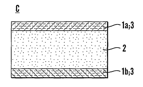
processing applications, as shown in fig. 1. The memory circuit C comprises
first
10 and second electrodes 1 a;1 b interfacing a memory material 2, in this case
a
ferroelectric polymer sandwiched between two electrodes in a parallel-plate
capacitor-like structure. By applying a voltage signal between the electrodes,
the
ferroelectric polymer is subjected to electrical fields that may affect or
interrogate
its polarization state. Although claimed to be generally applicable for
organic and
polymeric electrets and ferroelectrics, the subsequent discussion shall
primarily
treat polymeric ferroelectrics, with emphasis on PVDF and its co- and/or ter-
polymers with TrFE and/or TFE. This in order to provide focus and concreteness
to the presentation and to encompass classes of materials that appear of
particular relevance for future devices of interest.
Based on experimental and theoretical evidence, the inventors have found that
a
generally recurring, ubiquitous and dominant mechanism for fatigue and imprint
is redistribution of charged impurity species in the bulk of the ferroelectric
polymer and near the electrode regions, under the influence of electrical and
chemical potentials. Upon arriving at the ferroelectric/electrode interface,
such
impurities may be captured by deep traps at the ferroelectric/electrode
interface
or react chemically with the electrode material. The impurities may create
reaction products, which form insulating barrier layers at the electrodes and
traps for ionic species that subsequently arrive at the electrodes. Depending
on
the depth of the traps, localized charges may build up at the electrode
surfaces
CA 02464082 2005-12-06
11
and damage the function of the cell by creating depolarization fields and thus
pinning of ferroelectric domains. Chemical reactions between ionic or neutral
species and electrodes may also destroy the physical integrity of the
electrodes
and render them non-functional by reducing their conductivity to unacceptably
low levels.
Thus, ferroelectric activity is lost by secondary effects associated with the
accumulation of defects at the electrodes or at the internal interfaces in the
bulk
of the ferroelectric memory material (i.e. domain boundaries, or boundaries
between amorphous and crystalline regions, or grain boundaries). These
defects, (e.g. ionic species) may either be present a priori as foreign
impurities
in the ferroelectric material from the synthesis or film manufacturing
process, or
be derived from the degradation of the ferroelectric due to various forms of
stress occurring during the manufacturing of the memory cells or subsequent
electrical or mechanical stresses relating to the operation of the devices.
The remedies found to be efficacious against the above deleterious phenomena
and which constitute the present invention to be described and exemplified
below, differ fundamentally from those developed for the above referred
inorganic ferroelectric memory films where volatile constituents, e.g. oxygen
in
PZT, are lost during the switching of the ferroelectric. In those cases,
remedies
are focused on filling vacancies by replacing lost species such as oxygen, and
by suppressing vacancy generation by doping or stoichiometric modification of
the bulk ferroelectric.
According to an embodiment of the present invention, the electrodes contacting
the ferroelectric are prepared so as to capture e.g. ions arriving at the
electrode/ferroelectric memory material interface, and to incorporate said
ions
into the electrode structure without loss of electrical conductivity in the
electrode
material. This is achieved by judicious selection of electrode materials,
where
each electrode may be a single monolithic sheet or film, or where each
electrode
CA 02464082 2005-12-06
12
is created as a sandwich structure containing two or more functional layers.
Desired functionalities of the overall electrode structure are as listed
below, viz.
i. Electrical conductivity.
ii. Trapping/incorporation of deleterious ionic species.
iii. Barrier activity against penetration of electrodes by impurities
migrating
towards the electrodes from the ferroelectric.
iv. Barrier activity against migration of charged or neutral species into the
ferroelectric from the electrodes.
Here, electrical conductivity ensures that ionic species arriving at the
electrodes
from the bulk ferroelectric memory material are neutralized. Thus charge is
not
allowed to accumulate, which could create strong local domain pinning fields
or
significant depolarizing fields in the bulk ferroelectric. Incorporation of
ions in the
electrode structure ensures that neutralized ions do not accumulate at the
electrode/ferroelectric interface, which otherwise could create a non-
conducting
barrier layer and even cause structural damage. Finally, good barrier
properties
provide protection against penetration of chemically aggressive impurities
from
the bulk ferroelectric that might chemically attack the backing electrode
material
or other constituents of the memory device, or less aggressive impurities that
could still cause damage by structural dislocation of parts of the device
(e.g.
pressure being exerted by evolved gas).
Fig. 2 shows a first preferred embodiment of a memory circuit according to the
invention, where a single electrode material provides all the most important
functionalities of the electrodes 1a, 1b. In this case the functional material
can
be considered distributed evenly in the electrode material. Alternatively the
functional material 3 can be provided in a portion of the electrode material
in an
electrode 1 a;1 b. This portion must then extend to the surface of the
electrode
1 a;1 b contacting the ferroelectric memory material 2 of the memory cell in
order
to have the intended effect. In this case two or more functional material can
be
provided in respective strata of this portion, i.e. provided in a stratified
CA 02464082 2005-12-06
13
arrangement in the electrode material. From the above it will be seen that in
the
first embodiment the incorporation of the functional material in the electrode
material proper eliminates the need for using separate and distinct
interlayers of
functional material, as is the case of the second embodiment as respectively
shown in figs. 3 and 4. The actual provision of electrodes 1 a,1 b
incorporating
the functional material 3 in the first embodiment may entail more difficult
processing problems than is the case of a second embodiment described in the
following. The process requirements for providing the various materials and
layers in the memory circuit according to the invention shall, however,
briefly be
discussed further below. Clearly, this first embodiment requires electrode
material of exceptional qualities, but as shall be exemplified below, such
materials exist.
Fig. 3 shows a memory circuit according to a second preferred embodiment of
the invention. It has a capacitor-like structure where the different desired
functionalities of the electrodes 1 a, 1 b are taken care of by two separate
interlayers 3a;3b of functional material 3. These interlayers 3a;3b are
sandwiched between the electrodes 1 a;1 b and the memory material 2. The
interlayers 3a;3b comprise functional material 3 which is electrically
conducting
and which can incorporate into its structure without loss of electrical
conductivity
ionic species that migrate to the electrodes 1a;1b from the ferroelectric
memory
material 2 of the memory cell C. A highly conducting electrode material forms
the electrodes 1 a;1 b and provides good electrical connectivity to external
driving
and sensing circuits. The electrodes 1 a;1 b are coated with a conducting ion
trapping functional material 3 forming the interlayers 3a;3b on the side
facing the
ferroelectric memory material 2. The ion trapping layers 3a;3b exhibit good
barrier properties against the ionic species such that penetration and
chemical
attack on the backing electrode material and possibly other constituents of
the
memory circuit C are prevented. This separation of functionalities in
different
interlayers may be extended to structures containing more layers still, thus
widening the range of electrode materials that may be used and improve
CA 02464082 2005-12-06
14
performance and/or manufacturability. For instance may the interlayers 3a;3b
be
constituted by a number of sublayers respectively, each comprising a specific
functional material and hence tailored to a specific function such as one of
those
listed under ii) - iv) in page 9.
A variant of the second preferred embodiment of a memory circuit according to
the invention is shown in fig. 4, depicting the use of two separate
interlayers
3a;4a and 3b; 4b on either side of the memory cell C. The interlayers 3a,3b
facing the ferroelectric memory material 2 are electrically conducting and
have
the ability to absorb impurities from the ferroelectric memory material 2. The
interlayers 4a,4b likewise comprise a functional material 3 which is
conducting
and has good barrier properties, preventing the transfer of impurities through
to
the electrode layers 1 a,1 b, which are highly conducting material, e.g. a
metal
providing connection to other parts of the circuitry in the device. The latter
could
advantageously be the conductor material used in other parts of the same
device, to simplify the manufacturing process.
The operating principle of a functional material shall now be described in
some
detail. Ionic and neutral impurity species can be incorporated into the
electrode
structure in several ways, as illustrated schematically in figs. 5a, 5b and
5c.
Substitution, as shown in fig. 5a (i) and fig. 5a (ii) implies that the
impurity
dislodges a native constituent of the functional material and takes its place.
The
freed native constituent in its turn may migrate to another site where it is
bound
anew, e.g. by any of the mechanisms depicted in either these figures or the
following figs. 5b, 5d. Fig. 5b(i) and fig. 5b(ii) show incorporation by the
filling of
a vacancy, and fig. 5c(i) and fig. 5c(ii) interstitial placement. In all of
these cases,
it should be noted that a certain mobility exists for atoms and vacancies in
the
functional material. Thus, even a dense material with good barrier properties
may accommodate impurities in depth, i.e. beyond its first monolayer at the
interface against the ferroelectric memory material 2, through atomic and
molecular rearrangement.
CA 02464082 2005-12-06
The strategies described above implicitly restrict the range of acceptable
manufacturing processes providing the memory cell of ferroelectric memory
material 2 either with electrodes 1 a,1 b including a functional material 3 or
alternatively with interlayers 3a,3b of the functional material 3, as well as
the
materials and processes that may be chosen for creating the device as such.
Thus, harsh cleaning and coating procedures that create high incidence of
impurities or chemical and physical defects at the various layer or material
interfaces must be avoided.
Clearly, there must be a limit to the amount of impurities that can be
10 incorporated into the electrode structure before it starts to lose its
desirable
properties. However, it is worth noting that extension of device life, not
necessarily infinite time to failure, is what is sought for in most cases.
Also, in
many instances the main problem may be due to an initial population of
impurities originating from the materials synthesis or device manufacturing
process. When swept up and accommodated either in the electrode, or in a
separate interlayer this population ceases to be a problem, permitting stable
operation of the device for an extended period thereafter.
Advantageously the functional material or materials should have electrical
and/or chemical properties compatible with those of the electrode material and
this applies irrespective of whether the functional material is provided
distributed
in the electrode material or as a surface layer thereof. The implication is
particularly that the functional material shall be chemically compatible with
,
regard both to the electrode material and a ferroelectric or electret memory
material. This also means that the functional material after incorporation of
migrating atomic or molecular species from either the electrode material
proper
or the memory material still should retain its original electrical and
chemical
properties and particularly appear as compatible in either sense with both the
electrode material and the memory material. It will also commonly be required
that the functional material or the the functional materials as used, whether
CA 02464082 2005-12-06
16
distributed in the electrode material and particularly when provided as
surface
layers thereof, or provided as interlayers between the electrode and the
memory
material, should have a high-frequency relative permittivity that is about
equal to
or longer than that of the memory material so as to avoid the electrical
attenuation between a memory material and an electrode material. Although
conducting, the relative permittivity of a functional material could be
appreciably
less than that of the electrode material, but preferably higher than the
ferroelectric memory material and this property should remain unchanged when
migrating atomic or molecular species are incorporated. Neither should the
conductivity of the functional material change upon an incorporation of this
kind.
The memory circuit according to the present invention could be employed as
memory circuits in a matrix-addressable array of such memory circuits. In
other
words they would constitute a passive matrix-addressable memory device as
shown in plan view in fig. 6a and in cross section taken along line X-X in
fig. 6b.
The memory device is termed a passive matrix device since there are no
switching transistors connected to a memory circuit for switching a memory
cell
C on and off in an addressing operation. This would imply that the memory
material of the memory cell C in its unaddressed state has no contact with any
of the addressing electrodes of the matrix-addressable device. Basically a
memory device of this kind is formed with a first set of parallel strip-like
electrodes 1 b, which in fig. 6b is shown located on a substrate and covered
by
an interlayer 3b of functional material followed by a global layer of
ferroelectric
memory material, i.e. a ferroelectric polymer 2, which in its turn is covered
by a
global layer 3a of functional material over which are provided another
electrode
set comprising likewise parallel strip-like electrodes 1a, but oriented
orthogonally
to the electrodes 1 b, so as to form an orthogonal electrode matrix. The
electrodes 1a can e.g. be regarded as the word lines of a matrix-addressable
memory device, while the electrodes 1 b can be regarded as the bit lines
thereof.
At the crossings between the word lines 1 a and bit lines 1 b a memory cell is
defined in the matrix in the global layer of memory material 2. Thus the
memory
CA 02464082 2005-12-06
17
device will comprise a plurality of memory circuits C corresponding to the
number of electrode crossings in the matrix. The memory circuit C is shown in
more detail in cross section in fig. 6c and corresponds to the second
preferred
embodiment of the memory circuit according to the present invention. In other
words the functional material 3 is provided in respective interlayers 3a, 3b
which
interfaces respectively electrodes 1 a and 1 b with the memory material 2
sandwiched therebetween. It shall be understood that a memory device of the
kind shown in fig. 6a and 6b can be provided with an insulating layer over the
electrodes 1 a (or a so-called separation layer) and then a second similar
device
can be stacked on the top thereof and so on to form a stacked or volumetric
memory device as known in the prior art. It is to be understood that
electrodes
1 a, 1 b forming the respectively word and bit lines in the memory device in
fig 6a
all will be connected with suitable driving and control and sensing circuits
for
performing write/read operations to the memory cells of the matrix-addressable
memory device, although the peripheral external circuitry is not shown in the
drawing figures.
Providing a functional material in a matrix-addressable memory device of this
kind requires some attention to production detail. For instance the bit line
electrodes 1 b could be located on a substrate S and initially deposited as a
global layer covering the substrate whereafter the electrodes are patterned
e.g.
in a standard photolithographic process to form the strip-like bit line
electrodes
1 b. Alternatively parallel recesses with a cross section corresponding to an
electrode 1 b could be formed in the substrates and then filled with
appropriately
processed electrode material which if required could be planarized until the
electrode top surfaces become flush with that of the substrate. When the
functional material 3 is incorporated in the electrode material, a physical or
chemical vapour deposition can be employed to deposit both materials in order
to achieve a simultaneous or gradual incorporation of functional material in
the
electrode material. Alternatively, in following separate steps either a layer
3b or
functional material could be laid down as a global layer in the memory device
CA 02464082 2005-12-06
18
and then the global layer 2 of memory material is deposited before another
global layer 3a of functional material is provided covering the global layer
of
memory material 2. Finally word line electrodes 1 a are provided as shown in
fig.
6a and possibly covered by a planarization layer with insulating and
separating
function. The resulting structure is of course a memory device integrating a
plurality of memory circuits C according to the present invention in a passive
matrix-addressable memory array. When the functional material 3 is provided in
respective interlayers 3a, 3b both these layers as well as the memory material
2
are provided as global, i.e. unpatterned layers in the memory device, thus
allowing the integration of a single memory circuit into an array of such
memory
circuits the number of which can run into tens or hundred of millions or even
more with the capacity to store the same number of bits as a predetermined
polarization state or value of each separate memory circuit. Moreover, a
matrix-
addressable memory device of this kind can by suitable arrangement of the
external circuitry for write and read perform a write or read operation on a
hugely
massive parallel scale.
Various examples of functional materials which can be used in the memory
circuit according to the invention shall now be given, with explicit
descriptions of
functional material or interlayers thereof that are suited for use with
fluorine-
containing memory materials. This emphasis is based on the fact that certain
fluorine-containing polymeric ferroelectrics, in particular PVDF and
copolymers
of VDF and TrFE show particular promise as memory materials in future data
storage devices. It is also a fact that fluorine-containing memory materials
pose
exceptional challenges due to the mobility and chemical aggressiveness of
fluorine and hydrogen fluoride in neutral as well as ionic form.
Example 1: Electrodes with a diamond-like nanocomposite (DLN) film
During recent years, a new type of films have been developed where very good
corrosion resistance and barrier properties are combined with an electrical
conductivity which can be adjusted over 18 orders of magnitude by varying the
CA 02464082 2005-12-06
19
composition during film growth (cf., e.g. "Method for forming Diamond-Like
Nanocomposite or Doped-Diamond-Like Nanocomposite Films", US Patent No.
5,352,493 (1994); (Veniamin Dorfman and Boris Pypkin)). Termed Diamond-
Like Nanocomposite (DLN) carbon film, these films are somewhat similar to the
more well-known diamond-like carbon (DLC) films (cf., e.g. "Method of forming
Diamond-like Carbon Coating in Vacuum", International published application
W098/54376 (A.I. Maslov & al.), but consists of interpenetrating random
networks of predominantly diamond bonded carbon stabilized with hydrogen,
and glass-like silicon stabilized by oxygen. This C-Si self-stabilized
amorphous
structure forms the matrix for introduction of metals which form a third
interpenetrating network that can provide resistivities down to 10e-4 S2cm.
Depending on the desired properties, metals can be selected from a wide range
including Li, Ag, Cu, AI, Zn, Mg, Nb, Ta, Cr, Mo, W, Rh, Fe, Co, and Ni. These
films can be deposited at high rate on almost any substrate material,
subjecting
the latter to only mild temperature rise (room temperature deposition
temperature). Adhesion is good to virtually all materials of relevance in the
present context, i.e. inorganic as well as organic and polymeric materials for
use
as electrodes and ferroelectrics (e.g.: metals, oxides, ceramics, plastics).
Good
observed adhesion to Teflon is relevant in connection with the chemically
closely
related polymeric ferroelectrics such as PVDF and its copolymers with TrFE.
An important feature of DLN films is the possibility to tailor microstructural
as
well as chemical properties to each given application. As an example, consider
the problem of incorporation of aggressive species that migrate from the
ferroelectric towards an electrode surface consisting of DLN. As described in
the
above-referred literature, the DLN contains a web of interpenetrating sub-
networks. These sub-networks may be chosen so as to fulfil different
requirements of the electrode structure, i.e. structural integrity, barrier
properties, electrical conductivity and accommodation of impurities from the
ferroelectric memory material.
CA 02464082 2005-12-06
Consider, specifically the structure of DLN film as shown in fig. 7. One
network
consists of predominantly spa bonded carbon stabilized by hydrogen,
constituting a structural backbone. Another network consists of silicon
stabilized
by oxygen, intertwined with the C-H network and together with the latter
providing mechanical strength and barrier properties for the overall electrode
structure. Thirdly, there is a network of dopant elements or dopant compounds
with elements selected from groups 1-7b and 8 of the periodic system. These
dopants are accommodated in a network of nanopores formed in between the
other two networks and are in this case a metal at a density above the
10 percolation limit, providing electrical conductivity and adding to the
barrier
properties of the combined network structure. Other dopants may also be
incorporated in a controlled manner during the DLN manufacturing process; thus
dopant concentration gradients within the depth of the film may be created.
Assume now that the impurities to be dealt with are, e.g., F- ions and
hydrogen
fluoride, which would be of relevance in connection with PVDF and P(VDF-
TrFE) ferroelectrics. Upon arriving at the electrode interface represented by
the
DLN film, the impurities would enter the nanopore network and become
immobilized there. Trapping inside the network may take place by any of the
generic mechanisms illustrated in figs. 5a-c. As is apparent to persons
skilled in
20 physics and chemistry, the structure in fig. 7 offers an extraordinary
range of
opportunities for selecting preferred trapping mechanisms. Typically, deep
traps
are desired for permanent immobilization. One way of achieving this is to
provide sites inside the electrode material that exhibit strong chemical
reactivity
with the impurity species, e.g. fluorine, and where the reaction product
remains
locked into the structure with no deleterious effects on the functionality of
the
electrode. In the example here, one notes that not only dopants in the
nanopore
network, but also the oxygen-stabilized silicon network itself can serve as
sacrificial reactive species in the electrode structure. For example, HF acid
is
known to selectively etch the Si-O network in DLN (cf. V.Dorfman: "Diamond-
like
nanocomposites (DLN)", Thin Solid Films 212 267-273 (1992).
CA 02464082 2005-12-06
21
Example 2: Conducting carbide as functional material
The transition metal carbides have high melting points, show good wear
resistive properties and are chemically stable. Many of the transition metal
nitrides are also good conductors. Here, emphasis is made on tantalum carbide
(TaC), titanium carbide (TiC), zirconium carbide (ZrC) and hafnium carbide
(HfC). Especially TiC is of interest to combine with the present Ti
electrodes.
These compounds forms in the NaCI structure and have a complex combination
of metallic, covalent and smaller amounts of ionic bonds. The resistivity
depends
on the crystalline perfection and is typically 30 - 50~10-$ S2m.
Thin films of this material are typically formed using glow discharge
techniques
e.g. reactive magnetron sputtering. Methods to form good quality films are
well
developed and the materials are for instance, used as diffusion barriers, wear
resistive coatings, and optical coatings.
Example 3: Conducting oxide as functional material
This includes binary or ternary oxides, doped/undoped. Typical deposition
techniques are CVD/spin (Sn2O3:ln, Sn02:F, ZnO:AI) and sputtering (LSMO,
RuO, Ir02, ITO).
Example 4: Conducting boride as functional material
This includes HfB, ZrB, CrB.
Example 5: Conducting nitride as functional material
Nitride compounds have conductivities covering a wide range making the
materials metallic, semi-conducting or insulating. Especially the transition
metal
nitrides have attracted a large scientific interest. These materials have high
melting points, show good wear resistive properties and are chemically stable.
CA 02464082 2005-12-06
r
22
Many of the transition metal nitrides are also good conductors. Here, emphasis
is made on the group-4A nitrides; titanium nitride (TiN), zirconium nitride
(ZrN)
and hafnium nitride (HfN). Especially TiN is of interest to combine with Ti
electrodes. These compounds forms in the NaCI structure and have a complex
combination of metallic, covalent and ionic bonds. The resistivity depends on
the
crystalline perfection and is typically 20 - 30~10-$ S2m. Thin films of this
kind are
typically formed using glow discharge techniques, e.g. reactive magnetron
sputtering. Methods to form good quality films are well developed and the
materials are, for instance, used as diffusion barriers, wear resistive
coatings,
and optical coatings. In addition group-5A nitrides such as TaN, VN, NbN and
group-6A nitrides such as CrN may be used.
For relevant literature, see, e.g.: Transition metal carbide and nitrides by
Louis
E. Toth, Academic Press 1971; Papers by J.E. Greene, J.E. Sundgren, L.G.
Hultman, etc.
Example 6: Conducting polymer as functional material
The first highly conducting polymers were synthesized about 25 years ago with
the development (H. Shirakawa) of a silvery all-trans polyacetylene (PA) and
later doping (H. Shirakawa, E.J. Louis, A. G. MacDiarmid, C.K. Chiang and A.J.
Heeger; J. Chem. Soc. Chem. Comm. (1977) 579) of the same material using
e.g. 12. The conductivities in these films were found to be in the order of
103
(S2cm)-1. Soon it was also discovered that other conjugated polymers like
polyp-phenylene) (PPP), polypyrrole (PPy), polyp-phenylenevinylene) (PPV),
polythiophene (PT) and polyaniline (PANI) were possible to dope. However, a
drawback with these materials was that they were not processable.
In the middle of the 80's it was demonstrated that conjugated polymers could
be
processable (both soluble and meltable) when alkyl side chains were added to
polythiophene giving poly(3-alkylthiophene) (P3AT). Possibilities to dope
these
CA 02464082 2005-12-06
23
materials were also demonstrated (Sato, Tanaka, Kaeriyama; Synthetic Metals
18 (1987) 229), but the stability was poor (G. Gustafsson, O.Inganas,
J. O.Nilsson, B.Liedberg, Synthetic Metals 31 (1988) 297).
In the years to come the conducting polymers were further developed giving
material that were processable (e.g. polyaniline dodecylbenzenesulfonic acid,
PANI DBSA) and soluble (e.g. poly(ethylenedioxythiophene) with
polystyrenesulfonic acid, PEDOT-PSS) also in the doped state. Today
conducting polymers with conductivities ranging from 102(?) to 105 (S2cm)-1
are
commercialized for large number of applications.
Example 7: Conducting silicide as functional material
This includes TiSi2.
Example 8: Other types of functional materials
These include graphitic carbon, fullerenes such as C60 (buckminster fullerene)
and substances with a cyano entity (CN) as a functional group.
In the memory circuit according to the invention the memory material in the
memory cell is preferably a ferroelectric or electret memory material. This
material advantageously can be polyvinylidenedifluoride-trifluoroethylene
(PVDF-TrFE) which presently can be considered the most widespread and best
understood polymer memory material. The memory material shall be interfaced
between electrodes to form a complete memory circuit and these electrodes are
usually metallic, preferably made of aluminium, platinum, titanium, copper or
alloys of composites of these. The electrode material shall in any case
exhibit
good electrical conductivity. One problem in this connection that is well-
understood by persons skilled in the art and has been much discussed in the
literature is the need for providing the electrodes as a metallization
directly on
the polymer memory material which has inherently a much lower melting point
CA 02464082 2005-12-06
24
than the electrode material. Basically the same problem also appears when the
functional materials according to the invention of the various preferred types
discussed above shall be provided in the memory circuit of the invention. This
problem manifests itself somewhat differently depending on the actual further
embodiment to be realized. Generally the electrode material of a first
electrode,
say 1 a, is provided in the memory circuit, e.g. by being deposited on a not
shown substrate by means of physical or chemical vapour deposition. In the
first
embodiment shown in fig. 2 the functional material can then be included also
in
a similar vapour deposition process resulting in the formation of an electrode
1 a
comprising the functional material evenly distributed in the electrode
material. As
an alternative, unmixed electrode material in an initial stage of the process
deposited by physical or chemical vapour deposition as before, whereafter a
functional material is added in increasing amounts in following process
stages.
The deposition of more than one functional material can then take place in
different process stages resulting in a stratified or graded distribution of
these
materials in a portion of the electrode material adjacent to its surface where
a
subsequent deposition of the memory material can take place by spin- or dip-
coating processes. Since the memory material with its low melting point now is
deposited on a solidified layer of electrode material incorporating one or
more
functional materials, there usually will be' no problems in a subsequent
process
step with either thermal or chemical compatibility. However, when a second
electrode e.g. 1 b with one or more admixed functional materials shall be
deposited on the polymer memory material, special care should be taken to
avoid this further deposition process having detrimental influences on the
already provided polymer memory material. Thus physical or chemical vapour
deposition involving a low thermal input flux into the polymer material should
be
used when forming the initial film of either electrode or functional material
on the
surface of the polymer memory material. For instance, the input of thermal
energy to the polymer memory material in this stage could be kept well below a
certain value to avoid build-up of thermal energy in a volume element of the
memory material exceeding the heat of fusion thereof.
CA 02464082 2005-12-06
Once the memory material is coated by an initial thin film of either
functional
material or electrode material or an admixture therewith, the deposition
process
can continue with reliance on sufficient heat dissipation capacity in the
already
laid-down thin film such that the memory material is no longer detrimentally
influenced. It should be noted that the above processual considerations
generally apply irrespective of whether the functional material is provided
admixed in the electrode material or laid down in a separate process forming a
surface layer thereof or interlayers between the electrodes and the memory
material, as e.g. shown in fig. 3. It should also be noted that the functional
10 material can be deposited by means as briefly mentioned in conjunction with
example 2 or example 5 above.
When a conducting polymer is used as a functional material this cannot be
admixed with conventional, i.e. metallic, electrode material, but shall in any
case
be deposited at the surface thereof, thus forming an interlayer in the memory
circuit of the invention. As mentioned in the introduction of the application
and
according to the prior art, attempts have been made using conducting polymer
as the sole electrode material, i.e. thus avoiding metallic electrodes all
together.
Since, however, the conducting polymer will be chemically different from that
of
a polymer memory material, there may still be a possibility of a deterioration
of
20 either due to migration of mobile charged and/or neutral particles between
either, the prevention of which being a major objective of the present
invention.
Hence in the case of employing electrodes of conducting polymer material only,
the functional material advantageously can be incorporated in electrodes of
this
kind as dopants thereof, such that the electrodes now completely integrate the
required conduction and charge transfer functions with the desired effects of
a
functional material, viz. the incorporation of atomic or molecular species
contained in either the electrode material or the memory material and prone to
migration therebetween.
CA 02464082 2005-12-06
26
Finally it should be noted that it also may be possible to avoid complications
involved in a conventional metallization or deposition process for refractory
electrode material by providing the second electrode with a functional
material
either incorporated or with one or more surface layers thereof in the third
process step, involving the use of an additional not shown substrate or
backplane of e.g. a suitable electrically insulating material, whereafter the
second electrode layer and/or the functional material layers as applicable are
laminated to the memory material in a low-temperature process. This could be
particularly advantageous when also considering the fact that any diffusion of
a
functional material and/or electrode material into the memory material then
can
be largely eliminated.
As known to persons skilled in the art it should be understood that all layers
of
the memory circuit irrespective of whether they are electrode layers, a memory
material layer or interlayers of functional material, can be deposited as thin
films
by any of the deposition processes mentioned herein. This should be obvious to
persons skilled in the art and highly relevant, as e.g. ferroelectric memories
based on organic material such as ferroelectric polymers are today envisaged
as nothing but thin-film devices.