Note: Descriptions are shown in the official language in which they were submitted.
CA 02464604 2004-04-16
ORGANIC LUMINESCENT COMPOUNDS AND
METHODS OF MAKING AND USING SAME
FIELD OF THE INVENTION
The invention relates to organic compounds having luminescent properties, and
to
methods of synthesizing and using such compounds. The invention more
particularly relates to
compounds having photoluminescent and/or electroluminescent properties, and to
synthesis and
uses of same. The invention also relates to compounds having photo-receptor
properties due to
their ability to separate charges. The invention also relates to compounds
having photon
harvesting properties. The invention also relates to compounds that visibly
display detection of
metal ions or acid. The invention further relates to compounds that can
provide a molecular
switch.
BACKGROUND OF THE INVENTION
Production of devices based on electroluminescent display is a rapidly
growing, billion
dollar industry. Bright and efficient organic light-emitting diode (OLED)
devices and
electroluminescent (EL) devices have attracted considerable interest due to
their potential
application for flat panel displays (e.g., television and computer monitors).
OLED based displays
offer advantages over the traditional liquid crystal displays, such as: wide
viewing angle, fast
response, lower power consumption, and lower cost. However, several challenges
still must be
addressed before OLEDs become truly affordable and attractive replacements for
liquid crystal
based displays. To realize full color display applications, it is essential to
have the three
fundamental colors of red, green, and blue provided by emitters with
sufficient color purity and
sufficiently high emission efficiency.
In general, when a potential is applied across an OLED, holes are said to be
injected from
an anode into a hole transporting layer (HTL) while electrons are injected
from a cathode into an
electron transporting layer (ETL). The holes and electrons migrate to an
ETL/HTL interface.
Materials for these transporting layers are chosen so that holes are
preferentially transported by
the HTL, and electrons are preferentially transported by the ETL,. At th.e
ETL/HTL interface, the
holes and electrons recombine to give excited molecules which radiatively
relax, producing an
EL emission that can range from blue to near-infrared (Koene, 1998).
CA 02464604 2004-04-16
In providing one of the key color components for electroluminescent display
devices, blue
luminescent compounds are among the mast sought-after materials by industry
around the world.
Two alternative ways in which blue luminescence can be achieved are: (i)
providing a molecule
which emits blue color (emitter), and (ii) doping an emitter such that the
combination yields blue
luminescence. Conveniently, the emitter can be an inorganic metal ion such as,
for example,
lanthanide, which emits blue light via d to f or f to f electronic
transitions, or an organic molecule
which has conjugated ~t bonds and emits blue light via ~ to ~ or ~ to ra
electronic transitions.
A common problem with blue emitters is their lack of fang term stability in
OLEDs.
OLEDs generally suffer from a gradual intensity decrease of the blue hue,
which results in
gradual deterioration of the color purity of the display, and ultimately
failure of the device.
Television and computer monitors must perform consistently for at least five
years in order to be
commercially feasible. Even this modest expectation is a big challenge for
currently available
OLEDs.
There are several blue luminescent inorganic coordination compounds known
(U.S.
Patent No. 6,500,569, U.S. Patent No. 6,312,835, Yang, 2001, Jia et al.,
2003); however, in
some cases, due to a propensity for oxidation and/or hydrolysis reactions,
such complexes are not
very stable in solution. One family of known inorganic blue emitters,
lanthanide ions, have low
emission efficiency and require the use of a host (generally an inorganic
salt), which mazes it
difficult to process them into thin films.
Thus, blue luminescent materials that are organic in nature are desirable due
to their
increased stability, solubility and ability to form thin films. A number of
organic blue emitters
axe known to date (Shirota, 2000, Yang, 2001, Wu et al., 2001, and Liu et al.,
2000). Many of
these have poor luminescence efficiency and poor stability. Some are
luminescent polymers that
are difficult to apply in films using chemical vapor deposition (CVD) or
vacuum deposition,
processes known to produce superior films for electroluminescent displays.
Even the best blue
emitters currently available do not have the long term stability desired for
commercial devices.
The limitations discussed above could restrict the market for OLED products,
despite
their many superior aspects as compared with liquid crystal displays.
Therefore, in order for
OLEDs to become truly feasible, there is a need for stable, organic emitters.
BRIEF STATEMENT OF THE INVENTION
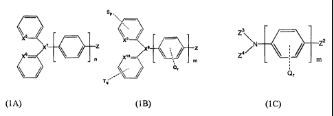
In a first aspect, the invention provides a compound having a general formula
(lA):
2
CA 02464604 2004-04-16
XB_ X, a i Z
n
(lA)
where X5, X6 and X' are each independently selected from the group consisting
of carbon and
nitrogen;
n is a number from 0-2;
Z is a substituted or unsubstituted aryl moiety selected from the group
consisting of
phenyl, biphenyl, naphthyl, anthryl, phenanthryl, pyrenyl, pyridyl, bipyridyl,
indyl, and
quinolinyl; and
wherein a said substituent is selected from the group consisting of an aryl
group, an
alkoxy group, a hydroxy group, a halo group, an amino group, a vitro group, a
nitrile group, -CF3
and an aliphatic group having 1-24 carbon atoms which may be straight,
branched or cyclic.
In some embodiments, X5, X6 and X' may be each independently selected from the
group
consisting of a substituted carbon, an unsubstituted carbon and an
unsubstituted nitrogen. In
some embodiments, at least one of X5, X6 and X' is nitrogen. In some
embodiments, X5, X6 and
X' are nitrogen.
In a second aspect, the invention provides a compound having a general formula
( 1 B):
SP
Z
n
Tq
(1B)
where Xg, X9 and X'° are each independently selected from the group
consisting of a
3
CA 02464604 2004-04-16
substituted or unsubstituted carbon, an unsubstituted nitrogen and a
substituted or unsubstituted
silicon;
m is a number from 0-10;
Q, S and T are the same or different and are selected from the group
consisting of an aryl
group, an alkoxy group, a hydroxy group, a halo group, an amino group, a nitro
group, a nitrite
group, -CF3 and an aliphatic group having 1-24 carbon atoms which may be
straight, branched or
cyclic;
p and q are the same or different and are a number between 0-~;
r is a number between 0-4;
Z is a substituted or unsubstituted aryl moiety selected from the group
consisting of
phenyl, biphenyl, naphthyl, anthryl, phenanthryl, pyrenyl, pyrid;yl,
bipyridyl, indyl, and
quinolinyl;
wherein a said substituent is selected from the group consisting of an aryl
group, an
alkoxy group, a hydroxy group, a halo group, an amino group, a vitro group, a
nitrite graup, -CF3
and an aliphatic group having 1-24 carbon atoms which may be straight,
branched or cyclic.
In some embodiments, Xg is selected from the group consisting of a substituted
or
unsubstituted carbon, an unsubstituted nitrogen and a substituted or
unsubstituted silicon; X9 and
X'° are each independently selected from the group consisting of a
substituted or unsubstituted
carbon and an unsubstituted nitrogen; and m is a number from 0 to 4. In some
embodiments, X$
is nitrogen; X9 and X'° are each independently selected from the group
consisting of a substituted
or unsubstituted carbon and an unsubstituted nitrogen; and m is a number from
1 to 4.
In a third aspect, the invention provides a compound having a general formula
( 1 C):
Z3
jN Z2
m
Q~
( 1 C)
where Z2, Z3 and Z4 are each independently a substituted or unsubstituted aryl
moiety selected
from the group consisting of phenyl, biphenyl, naphthyl, anthryl, phenanthryl,
pyrenyl, pyridyl,
bipyridyl, indyl, and quinolinyl;
m is a number from 0-10;
Q is selected from the group consisting of an aryl group, an alkoxy group, a
hydroxy
4
CA 02464604 2004-04-16
group, a halo group, an amino group, a nitro group, a nitrite group, -CF3 and
an aliphatic group
having 1-24 carbon atoms which may be straight, branched or cyclic;
r is a number between 0 and 4;
wherein a said substituent is selected from the group consisting of an aryl
group, an
alkoxy group, a hydroxy group, a halo group, an amino group, a nitro group, a
nitrite group, -CF3
and an aliphatic group having 1-24 carbon atoms which may be straight,
branched or cyclic.
In another aspect, the invention provides a photoluminescent or
electroluminescent
compound having a formula selected from the group consisting of 1-pyrenyl-2,2'-
dipyridylamine
(2), 4-(1-pyrenyl)phenyl-2,2'-dipyridylamine (3), 4-[4'-(1-pyrenyl)biphenyl]-
2,2'-dipyridylamine
(4), 4-(1-pyrenyl)biphenyl-2,2'-diphenylamine (5) and QNPB (6).
Compounds of the invention may be photoluminescent and/or electroluminescent.
Compounds of the invention may be hole transporters.
In further aspect, the invention provides a method of synthesizing a compound
of general
formula (lA), comprising a step selected from the group consisting of
1-bromopyrenyl + 2,2'-dipyridylamine + CuI + K3P04+ 1,2-
transdiaminocyclohexane + 1,4-dioxane
1-pyrenyl-2,2'-dipyridylamine (2);
Pd(PPh3)4 + 1-brornopyrene +p-(2,2'-dipyridylamino)phenyl boronic acid
4-( 1-pyrenyl)phenyl-2,2'-dipyridylamine(3 );
Pd(PPh3)4 + 1-bromopyrene + p-(2,2'-dipyridylamino)biphenylboronic acid
4-[4'-(1-pyrenyl)biphenyl]-2,2'-dipyridylamine(4);
4-iodo-4'-diphenylaminobiphenyl + B(OCH3)3 + N-BuLi
4-(1-pyrenyl)biphenyl-2,2'-diphenylamine (5); and
p-N-(1-naphthyl)-N-phenylamino-biphenyl-iodide + B(i-OPr)3 + N-BuLi
p-N-(1-naphthyl)-N-phenylamino-biphenyl-B(OH)2 + 5-bromo-8-
methoxyquinoline + Pd(OAc)2 + PPh3 + NazC03 ~ QNPB (6).
In further aspect, the inventian provides a method of synthesizing a compound
of general
___.___.. .~..~.. _~~ ..-~~.- ~..~-.~.~ ~ ..n _.~~...._-__-._._r___. __
CA 02464604 2004-04-16
formula (1B), comprising a step selected from the group consisting of
1-bromopyrenyl + 2,2'-dipyridylamine + CuI + K3P04+ 1,2-
transdiaminocyclohexane + 1,4-dioxane
1-pyrenyl-2,2'-dipyridylamine (2);
Pd(PPh3)4 + 1-bromopyrene +p-(2,2'-dipyridylamino)phenyl boronic acid
4-(1-pyrenyl)phenyl-2,2'-dipyridylamine(3);
Pd(PPh3)4 + 1-bromopyrene + p-(2,2'-dipyridylamino)biphenylboronic acid
3 4-[4'-(1-pyrenyl)biphenyl]-2,2'-dipyridylamine(4); and
4-iodo-4'-diphenylaminobiphenyl + B(OCH3)3 + N-Buhi
4-(1-pyrenyl)biphenyl-2,2'-diphenylamine (5).
In further aspect, the invention provides a method of synthesizing a compound
of general
formula (1C), comprising a step selected from the group consisting of
p-N-(1-naphthyl)-N-phenylamino-biphenyl-iodide + B(i-OPr)3 + N-BuLi
p N-(1-naphthyl)-N-phenylamino-biphenyl-B(OH)2 + 5-bromo-8-
methoxyquinoline + Pd(OAc)2 + PPh3 + Na2C03 -~ QNPB (6).
In further aspects, the invention provides compositions comprising a compound
of the
invention, an organic polymer and a solvent.
In still further aspects, the invention provides a photoluminescent product or
an
electroluminescent product comprising a compound of the invention. The product
may be a flat
panel display device. The product may be a luminescent probe.
In another aspect, the invention provides a method of producing
electroluminescence,
comprising the steps of providing an electroluminescent compound of the
invention and
applying a voltage across said compound so that said compound
electroluminesces.
In other aspects, the invention provides electroluminesce~nt devices for use
with an
applied voltage.
A first such device comprises: a first electrode, an emitter which is an
electroluminescent
6
CA 02464604 2004-04-16
compound of the invention, and a second, transparent electrode, wherein
voltage is applied to the
two electrodes to produce an electric field across the emitter so that the
emitter
electroluminesces.
A second such device comprises: a first electrode, a second, transparent
electrode, an
electron transport layer adjacent the first electrode, a hole transport layer
adjacent the second
electrode, and an emitter which is an electroluminescent compound of the
invention interposed
between the electron transport layer and the hole transport layer, wherein
voltage is applied to the
two electrodes to produce an electric field across the emitter so that the
emitter
electroluminesces.
A third such device comprises: a first electrode, a second, transparent
electrode, a layer
which is both an emitter and an electron transporter which is an
electroluminescent compound of
the invention and which is located adjacent the first electrode, and a hole
transport layer which is
interposed between the emitter and electron transport layer and the second
electrode, wherein
voltage is applied to the two electrodes to produce an electric field so that
the emitter
electroluminesces.
A fourth such device comprises: a first electrode, a secomd, transparent
electrode, a layer
which is all of an emitter, an electron transporter and a hole transporter
which is an
electroluminescent compound of the invention and which is interposed between
the first and the
second electrode, wherein voltage is applied to the two electrodes to produce
an electric field so
that the emitter electroluminesces.
A fifth such device comprises: a first electrode, a second, transparent
electrode, an
electron transport layer which is a compound of the invention and which is
located adjacent the
first electrode, a hole transport layer adjacent the second electrode, and an
emitter which is
interposed between the electron transport layer and the hole transport layer,
wherein voltage is
applied to the two electrodes to produce an electric field so that the emitter
electroluminesces.
A sixth such device comprises: a first electrode, a second, transparent
electrode, an
electron transport layer which is located adjacent the first electrode, a hole
transport layer which
is a compound of the invention and which is located adjacent the second
electrode, and an
emitter which is interposed between the electron transport layer and the hole
transport layer,
wherein voltage is applied to the two electrodes to produce an el,ectrie field
so that the emitter
electroluminesces.
A seventh such device comprises: a first electrode, a second, transparent
electrode, a layer
which is both an electron transporter and an emitter which is located adjacent
the first electrode,
and a hole transport layer which is a compound of the invention and which is
interposed between
7
_........__.._.___" "", s~.,rnaa,asw~ r.~~., ~s~aamawma, ~~aaxn~~~...._...
_~_~.__ ...,am,",A"~,., .._... .___._
CA 02464604 2004-04-16
the electron transport layer and the second electrode, wherein voltage is
applied to the two
electrodes to produce an electric field so that the emitter electroluminesces.
An eighth such device comprises: a first electrode, a second, transparent
electrode, an
electron transport layer which is located adjacent the first electrode, anal a
layer which is both an
emitter and a hole transporter which is a compound of the invention and which
is interposed
between the electron transport layer and the second electrode, wherein voltage
is applied to the
two electrodes to produce an electric field so that the emitter
electroluminesces.
In another aspect, the invention provides a method of detecting metal ions,
comprising the
steps of providing a photoluminescent compound of the invention, and detecting
photoluminescence of said compound, wherein contact with a metal ion quenches
said
photoluminescence of said compound. The metal ions may be selected from the
group consisting
of Zn2+, Cu2+, Ni2+y Cdz+, HgZ+ and Ag+.
In another aspect, the invention provides a method of detecting acid,
comprising the steps
of providing a photolutninescent compound of the invention, and detecting
photoluminescence
of said compound, wherein protonation of said compound changes the state of
said compound's
photoluminescence.
In another aspect, the invention provides a method of harvesting photons,
comprising the
steps of providing a compound of the invention, and providing light such that
photons strike
said compound and charge separation occurs in said compound. In some
embodiments, the
separated charges may recombine and photons be released. In some embodiments,
the separated
charges may migrate to respective electrodes to produce a potential
difference.
In another aspect, the invention provides a method of separating charges,
comprising the
steps of providing a compound of the invention, and providing light such that
photons strike
said compound and charge separation occurs in said compound. In some
embodiments, the
separated charges may recombine and photons be released. In some embodiments;
the separated
charges may migrate to respective electrodes to produce a potential
difference.
In other aspects, the invention provides a photocopier, a photovoltaic device,
a
photoreceptor, a solar cell and a semiconductor employing the afore-mentioned
methods of
harvesting photons and/or separating charges.
In another aspect, the invention provides a molecular switch comprising a
compound of
the invention that is capable of existing in more than one luminescent state,
wherein acid, base,
and/or incident light produces a change in the luminescent state of said
compound. The
invention further provides a circuit comprising such a molecular switch.
CA 02464604 2004-04-16
BRIEF DESCRIPTION OF THE DRAWINGS
For a better understanding of the present invention and to show more clearly
how it may
be carried into effect, reference will now be made by way of example to the
accompanying
drawings, which illustrate aspects and features according to preferred
embodiments of the present
invention, and in which:
Figure 1 shows a preferred embodiment of a three layer electroluminescent (EL)
display
device according to the invention.
Figure 2 shows the excitation (lower wavelength) and emission (higher
wavelength)
photoluminescence spectra of 1-pyrenyl-2,2'-dipyridylamine (2) as a solid.
Figure 3 shows the excitation (lower wavelength) and emission (higher
wavelength)
photoluminescence spectra of 1-pyrenyl-2,2'-dipyridylamine (2) in a CHZC12
solution at a
concentration of 2.55 x 10⁻⁶ M at 298K.
Figure 4 shows the excitation (lower wavelength) and emission (higher
wavelength)
photoluminescence spectra of 4-(1-pyrenyl)phenyl-2,2'-dipyridylamine (3) as a
solid.
Figure 5 shows the excitation (lower wavelength) and emission (higher
wavelength)
photoluminescence spectra of 4-(1-pyrenyl)phenyl-2,2'-dipyridylamine (3) in a
CHZC12 solution
at a concentration of 2.55 x 10⁶ M at 298K.
Figure 6 shows the excitation (lower wavelength) and emission (higher
wavelength)
photoluminescence spectra of 4-(4'(1-pyrenyl)biphenyl]-2,2'-dipyridylamine (4)
as a solid.
Figure 7 shows the excitation (lower wavelength) and emission (higher
wavelength)
photoluminescence spectra of 4-[4'-(1-pyrenyl)biphenyl]-2,2'-dipyridylamine
(4) in a CHzCl2
solution at a concentration of 2.55 x 10⁻⁶ M at 298K.
Figure 8 shows an electroluminescence spectrum produced by compound 4-(1-
pyrenyl)phenyl-2,2'-dipyridylamine (3) in a two layer EL device described in
Example 6.
Figure 9 shows the crystal structure of compound (2).
Figure 10 shows the crystal structure of compound (3).
Figure 11 shows the crystal structure of compound (4).
Figure 12 shows the (-) photoluminescence (PL) spectrum of compound (4) and
the
(- - -) electroluminescence (EL) spectrum of compound (4) produced by a solid-
state filin at
298K.
Figure 13 shows the dependence of Luminance (L) and Current Density (J) on
Voltage
(V) of a film of compound (4) in a two layer EL device of the following
configuration: TfO/NPB
(40 nm)/compound(4) (40 nm)/LiF (1 nm)/Al, where NPB is the hole transport
layer, compound
(4) is both the emitter and electron transport layer and LiF is added to
improve contact between
9
CA 02464604 2004-04-16
the electron transport layer and the cathode.
Figure 14 shows the excitation (lower wavelength) and the emission (higher
wavelength)
spectra of compound (5) as a solid-state film (-) at 298K and as a CHzCl2
solution (CI) at a
concentration of 10'S M at 298K.
Figure 15A is a cyclic voltametry diagram starting with the reduction of
compound (5) in
a mixture of CHZC12 and CH3CN. This figure provides information about the
Lowest Unoccupied
Molecular Orbital (LUMO) of the molecule and indicates promising electron
transport properties
of the molecule.
Figure 15B is a cyclic voltametry diagram starting with the oxidation of
compound (S) in
a mixture of CHZC12 and CH3CN. This figure provides information about the
Highest Occupied
Molecular Orbital (HOMO) of the molecule and indicates promising hole
transport properties of
the molecule.
Figure 16 shows the dependence of Luminance (L) and Current (I) on Voltage (V)
of a
single layer EL device of compound (4) prepared with the following
configuration:
ITO/compound (4) (60 nm)/LiF(0.5 nm)/Al(140nm), where compound (4) is the hole
transport
layer, emitter and electron transport layer and LiF is added to improve
contact between the film
and the cathode.
Figure 17A shows the dependence of Current Density (J) on Voltage (V) of a
film of
compound (6) in a single layer EL device of the following configuration:
ITO/compound (6) (90
nm)/LiF (0.5 nm)/Al, where compound (6) is all of electron transport layer,
emitter and hole
transport layer and LiF is added to improve contact between the film and the
cathode.
Figure 17B shows the dependence of Luminance (L) on Voltage (V) of a film of
compound (6) in a single layer EL device of the following configuration:
ITO/compound (6) (90
nm)/LiF (0.5 nm)/Al, where compound (6) is all of electron transport layer,
emitter and hole
transport layer and LiF is added to improve contact between the film and the
cathode.
Figure 18 shows the (-) photoluminescence spectrum of compound (6) and the (- -
-)
electroluminescence spectrum of compound (6) produced by a single layer EL
device of the
following configuration: ITO/compound (6) (90 nm)/LiF (0.5 nrn)/Al, where
compound (6) is all
of electron transport layer, emitter and hole transport layer and LiF is added
to improve contact
between the film and the cathode.
Figure 19A shows the dependence of Current Density (J) on Voltage ('~ of a
film of
compound (6) in a double layer EL device of the following configuration:
ITO/compound (6)
(30, 60, 90, 120 nm)/Alq3 (40 nm)/LiF (0.5 nm)/Al, where compound (6) is the
hole transport
layer and Alq3 is both emitter and electron transport layer and LiF is added
to improve contact
. ~..~.,. ~ . .. ~e..,~.,. . ~* ~ *.~~ fi .. . . ., m._. .....,.. . ___..-m_ .
. ..- _.~ . .u.~..m ._.__ _._..__.
."n.'~A4H d , . ~,.,R:r~.tR~'WC..34.n.n:y'e,.,Fi"X~a.e s~.~a~,urr'~~" vw.wemx
.R...a~.A..wrn.. ~ a..;..*myaww..n~
CA 02464604 2004-04-16
between the film and the cathode.
Figure 19B shows the dependence of Luminance (L) on Voltage (V) of a film of
compound (6) in a double layer EL device of the following configuration:
ITO/compound (6)
(30, 60, 90, 120 nm)/Alq3 (40 nm)lLiF (0.5 nm)/Al, where compound (6) is the
hole transport
layer and Alq3 is both emitter and electron transport layer and LiF is added
to improve contact
between the film and the cathode.
Figure 20 shows the crystal structure of (6).
Figure 21 is a cyclic voltammetry diagram starting with the oxidation of
compound (6) in
CHZCIz. This figure provides information about the Highest Occupied Molecular
Orbital
(HOMO) of the molecule and indicates promising hole transpou properties of the
molecule.
11
CA 02464604 2004-04-16
DETAILED DESCRIPTION OF THE INVENTION
In a first aspect of the invention, a stable organic compound of the general
formula (1A)
is provided:
x= ~
~" \ /
\ /
(lA)
where X5, X6 and X' are each independently selected from the soup consisting
of carbon and
nitrogen;
n is a number from 0-2;
Z is a substituted or unsubstituted aryl moiety selected from the group
consisting of
phenyl, biphenyl, naphthyl, anthryl, phenanthryl, pyrenyl, pyridyl, bipyridyl,
indyl, and quinolinyl
(preferred substituent examples la-lm are pictured below); and
wherein a said substituent is selected from the group consisting of an aryl
group, an
alkoxy group, a hydroxy group, a halo group, an amino group, a vitro group, a
nitrite group, -CF3
and an aliphatic group having 1-24 carbon atoms which may be straight,
branched or cyclic.
Preferably a compound of general formula (lA) exhibits intense luminescence,
which
may be photoluminescence and/or electroluminescence.
In preferred embodiments of compounds of the general formula (lA), X5, X6 and
X' are
each independently a substituted or unsubstituted carbon or an unsubstituted
nitrogen. In some
embodiments, one or two of X5, X6 and X' are nitrogen. In a preferred
embodiment, X5, X6 and
X' are all nitrogen. A synthetic scheme depicting the preparation of such
compounds is pictured
in Schemes 1 and 2; working examples of detailed synthetic procedures are
provided in
Examples 1 - 4.
12
CA 02464604 2004-04-16
/ \ ~ \
\ I / \ I /
1a 1-naphthyl 1b 2-naphthyl
1c 9-anthryl
1 d 9-phenanthryl
1e 1-pyrenyl ~t ~-pyrenyl ,g 4-pyrenyl
1 h biphenyl 1 i phenyl
13
CA 02464604 2004-04-16
/ ~ \
1j indyl 1k quinolinyl
~\N N~ ~ 1~ / N
1 L pyridyl 1 m 4, 4'-bipyridyl
14
_ ._. ._. ~ y_ F. . ._k.~ > _~> E,,.v7~ ~ ~..:">~g~~~a>~~.~ >.~ .n~.. _ _._..
.~x..~.m.>,.> , .~.mr_..._.._.___.~.a~ , ~~~.~.~.~~T. _.___ _~_.~.~~_x~
CA 02464604 2004-04-16
In another aspect of the invention, a stable organic compound of the general
formula (1B)
is provided:
s_
Z
n
Tq
(1B)
where Xg, X9 and X'° are each independently selected from the group
consisting of a
substituted or unsubstituted carbon, an unsubstituted nitrogen and a
substituted or unsubstituted
silicon;
m is a number from 0-10, preferably I-4, most preferably 2;
Q, S and T are the same or different and are selected from the group
consisting of an aryl
group, an alkoxy group, a hydroxy group, a halo group, an amino group, a vitro
group, a nitrite
group, -CF3 and an aliphatic group having I-24 carbon atoms which may be
straight, branched or
cyclic;
p and q are the same or different and are a number between 0-5;
r is a number between 0-4;
Z is a substituted or unsubstituted aryl moiety selected from the group
consisting of
phenyl, biphenyl, naphthyl, anthryl, phenanthryl, pyrenyl, pyridyl, bipyridyl,
indyl, and quinolinyl
(preferred substituent examples la-Im are pictured above); and
wherein a said substituent is selected from the group consisting of an aryl
group, an
alkoxy group, a hydroxy group, a halo group, an amino group, a vitro group, a
nitrite group, -CF3
and an aliphatic group having 1-24 carbon atoms which may be straight,
branched or cyclic.
Preferably a compound of general formula ( I B) exhibits intense luminescence,
which
may be photoluminescence and/or electroluminescence.
IS
CA 02464604 2004-04-16
A preferred embodiment of the invention, particularly for hole transporting
properties, is
described by the general formula (IB), where
X$ is nitrogen;
X9 and X'° are each independently selected from the group consisting of
a substituted or
unsubstituted carbon and an unsubstituted nitrogen; and
m is a number from 1-4.
Another preferred embodiment of the invention is described by the general
formula (1B),
where
X$ is selected from the group consisting of a substituted. or unsubstituted
carbon, an
unsubstituted nitrogen and a substituted or unsubstituted silicon;
X9 and X'° are each independently selected from the group consisting of
a substituted or
unsubstituted carbon and an unsubstituted nitrogen; and
m is a number from 0 to 4.
16
.._....._ _...__.__. . _., ,.,.~~r ,e_~,._~,~,,:~:~,~ ~,r~..,.~.~ _._._._
.._m....~~. ~._.._. ,.~.....: ...___..__ ._______.~.~.~,~..~
CA 02464604 2004-04-16
In another aspect of the invention, a stable organic compound of the general
formula (1C)
is provided:
Z3
N. a Z2
o ;~
~r
(1C)
where
m is a number from 0-10, preferably 1-4, most preferably 2;
Q is selected from the group consisting of aryl group, an alkoxy group, a
hydroxy group, a
halo group, an amino group, a nitro group, a nitrite group, -CF3 and an
aliphatic group having 1-
24 carbon atoms which may be straight, branched or cyclic;
r is a number between 0-4;
Z2, Z3 and Z4 may be the same or different substituted or unsubstituted aryl
moiety
selected from the group consisting of phenyl, biphenyl, naphthyl, anthryl,
phenanthryl, pyrenyl,
pyridyl, bipyridyl, indyl, and quinolinyl (preferred substituent examples la-
lm are pictured
above); and
wherein a said substituent is selected from the group consisting of an aryl
group, an
alkoxy group, a hydroxy group, a halo group, an amino group, a nitro group, a
nitrite group, -CF3
and an aliphatic group having 1-24 carbon atoms which may be straight,
branched or cyclic.
Preferably a compound of general formula (1C) exhibits intense luminescence,
which
may be photoluminescence and/or electroluminescence.
In a preferred embodiment of compounds of the general formula (1 C), Z3 is
phenyl, Z4 is
napthyl, m is 2 and ZZ is substituted quinolyl. A synthetic scheme depicting
the preparation of
such compound is pictured in Scheme 3; a working example of detailed synthetic
procedures is
provided in Example 5.
17
. . _ __ _ ....... , . ~.. ~u.,.. ~,"~~~ . ~._. a ~.~,,~. ...r~ ~ ...... _.
_.. _ .. __ _ ~....~.... . _.
CA 02464604 2004-04-16
As used herein "aliphatic" includes alkyl, alkenyl and alkynyl. An aliphatic
group may be
substituted or unsubstituted. It may be straight chain, branched chain or
cyclic.
As used herein "aryl" includes heteroaryl and may be substituted or
unsubstituted.
Preferred aryl groups for Q, S, and T are Z.
As used herein "unsubstituted" refers to any open valence of an atom being
occupied by
hydrogen.
As used herein "substituted" refers to the structure having one or more
substituents.
18
CA 02464604 2004-04-16
Scheme 1. Preparation of example compounds of the general formula (lA).
aPA, Cul, K3P04,
'~ N
N
Br H2N NH2 % ~S
Pd(PPh3)4, NaOH
N ~ B(OH)2
1 or 2
19
CA 02464604 2004-04-16
Scheme 2. Preparation of a further example compound of the general formula
(lA).
BULi, B~OMB)g ~-mvnwNycmc
..,...._< ~. , . __., ;, nw ~ ~ ..w. m." ~,. 2fiLWNe. ._,..;r-mnx,TJns ~z-r. ,
_ _,::n,urtit%
.wn..az~:~Fp'F%cn~rtwms:.d:~u4..,.:~.r.,w....a~v..__.___..«,.......m._.A.....~o
-..mn,a.....,.,.»..._,_,".,m._.".~.,..~.~u..",.."...sww.vr~,.mm~rcm~w~.,......-
.---,.___.. _.e. .w..~....>,:...».,9meur
CA 02464604 2004-04-16
Scheme 3. Preparation of an example compound of the general formula 1 C.
/ \ / ~ ~~ /
LiBu
N \ / \ ~~ ~ N \ / \ /
B(i-OPr)3
\ ~ \ /
Br
Pd(Otac)2
PPh3
NazCO 3 N
OMe
/
I \ / /_\ OMe
\ l \ iN
(6)
21
._.._ _ __ _ _._.._. ~~.~~. ~,...~,~: ~.~,~m _n___ __
CA 02464604 2004-04-16
Thus, the invention provides, for example, compounds 1-pyrerryl-2,2'-
dipyridylamine (2), 4-(1-
pyrenyl)phenyl-2,2'-dipyridylamine (3), 4-[4'-(1-pyrenyl)biphenyl)-2,2'-
dipyridylamine (4), 4-
(1-pyrenyl)biphenyl-2,2'-diphenylamine (5), and QNPB (6) which have the
following structures:
22
_ _ _._ ..~~..~~w . .._t~-~,. #._--_ __-~-
CA 02464604 2004-04-16
1-pyrenyl-2,2'-dipyridylamine (2)
/ \
N
N-_
(2)
23
CA 02464604 2004-04-16
4-(1-pyrenyl)phenyl-2,2'-dipyridylamine (3)
/ \
/ \ ~
N
N \ N
(3)
24
CA 02464604 2004-04-16
4-[4'-(1-pyrenyl)biphenyl]-2,2'-dipyridylamine (4)
(4)
CA 02464604 2004-04-16
4-(1-pyrenyl)biphenyl-2,2'-diphenylamine (5)
(5)
26
CA 02464604 2004-04-16
4-(1-naphthylphenylamino)-4'-(5-(8-methoxyquinolinyl))biphenyl (~NPB) (6)
'_ N ~ / ~ ~ ,_\ OMe
~ /N
(6)
27
CA 02464604 2004-04-16
(Note that this same substituent, 2,2'-dipyridylamine (dpa), is called
deprotonated di-2-
pyridylamine in U.S. Patents No. 6,500,569 and No. 6,312,835 by Borne of the
present inventors.)
The invention provides compounds that are photoluminescent and, in at least
some
embodiments of the invention, electroluminescent; they can produce intense
light.
The invention also provides a method of producing photoluminescence comprising
the
steps of providing a photoluminescent compound of the invention having a
formula as set out
above; and irradiating said photoluminescent compound with radiation of a
wavelength suitable
for exciting the compound to photoluminescence.
The invention further provides a method of producing electroluminescence
comprising
the steps of providing an electroluminescent compound of the invention having
a fomrmla as set
out above; and applying a voltage across said electroluminescent compound.
The invention further provides an electroluminescent device for use with an
applied
voltage, comprising: a first electrode, an emitter (e.g., phosphor) which is
an electroluminescent
compound of the invention, and a second, transparent electrode, wherein a
voltage is applied
between the two electrodes to produce an electric field across the emitter.
'The emitter
consequently eleetroluminesces. In some embodiments of the invention, the
device includes one
or more charge transport layers interposed between the emitter and one or both
of the electrodes.
For example, spacing of a preferred embodiment of the device, called for the
purposes of the
present specification a "three layer EL device", is: first electrode, first
charge transport layer,
emitter, second charge transport layer, and second, transparent electrode.
In certain embodiments of the invention, the device includes one or more
compounds of
the invention acting as one or more charge transport layers and~'or emitters)
interposed 'between
the electrodes.
In one embodiment of the invention, called for the purposes of the present
specification a
"two layer EL device", the spacing is: first electrode, charge transport
layer, emitter/second
charge transport layer, and second electrode. A working example of a two layer
EL device is
described in Example 6, refernng to Figure 8. Here, compound. 4-(1-
pyrenyl)phenyl-2,2'-
dipyridylamine (3) acted as both an emitter and a charge (electron) transport
layer.
In another embodiment of the invention, called for the purposes of the present
specification a "one layer EL device", the spacing is: first electrode, first
charge transport
layer/emitter/second charge transport layer, second electrode. A working
example of a one layer
EL device is described in Example 7, and luminance and current produced are
shown graphically
28
..,,.r .., . y" 5, n x.. ...... r.u.r..y_.,~ ' r~IR,rT,aF'z;:c . ,..,. ..,o..
rx:zwm. e........ . _.....~,...... ~ . . .....
. ~ki~ r'~~4GAP6~r~~"~W ~ASSeer.~.~" c.. ~ ~7....-~..~,».,-
.,.,.~......»..".a.,..":,....w,r... ...r...r....,.~._...-..-_ _ , .
_..__.._.....r..,w~.n..~~.w...~,.,..
CA 02464604 2004-04-16
in Figure 16. Similarly, the luminance and current density for a single layer
EL device of
compound (6) are shown graphically in Figures 17A and 17B.
An advantage of preferred compounds of the invention is that they are highly
soluble in
common organic solvents such as toluene, diethyl ether, tetrahydrofuran (THF),
and
dichloromethane. This permits the compounds to be blended easily and
conveniently with
organic polymers. The role of the organic polymer in such a mixture is at
least two-fold: First, a
polymer can provide protection for the compound from air degradation. Second,
a polymer host
matrix permits the use of a spin-coating or dip-coating process as an
alternative way to make
films. Although spin-coating and dip-coating processes may not produce as high
quality films as
those produced by chemical vapor deposition or vacuum deposition, they are
often much faster
and more economical.
Accordingly, the invention further provides methods of applying compounds as
described
above to a surface. These methods include solvent cast from solution,
electrochemical
deposition, vacuum vapor deposition, chemical vapor deposition, spin coating
and dip coating.
The compounds may be applied alone or with a carrier. In some embodiments of
the invention,
they are applied in a composition including an organic polymer. Such
compositions are also
encompassed by the invention.
As an example of this application, compounds of the invention are expected to
form a
clear transparent solution with the weakly luminescent polymer poly(N
vinylcarbazole) (PVK) in
CHZC12/C6HSC1. This can be converted to a transparent film by evaporating the
toluene solvent
via either a dip-coating or spin-coating process. Films obtained. in this way
are stable. (Jertain
polymers such as, for example, PVK, are expected to further enhance the
luminescence of an
emitter in the film.
The invention provides a method of producing electroluminescence comprising
the steps
of providing an electroluminescent compound of the invention having the
general formula (lA),
(1B) or (1C) as set out above; and applying a voltage across said
electroluminescent compound
so that the compound electroluminesces.
According to the invention, electroluminescent devices for use with an applied
voltage
are provided. In general, such a device has a first electrode, an emitter
which is an
electroluminescent compound of the invention, and a second, transparent
electrode, wherein a
voltage is applied between the two electrodes to produce an electric field
across the emitter of
sufficient strength to cause the emitter to electroluminesce. Preferably, the
first electrode is of a
metal, such as, for example, aluminum, which reflects light emitted by the
compound; whereas
the second, transparent electrode permits passage of emitted light
therethrough. The transparent
29
CA 02464604 2004-04-16
electrode is preferably of indium tin oxide (ITO) glass or an equivalent known
in the art. Here,
the first electrode is the cathode and the second electrode is the anode.
Referring to Figure 1, a preferred embodiment of an electroluminescent device
of the
invention is shown. The emitter is interposed between an electron transport
layer (e.g., tris-(8-
hydroxyquinoline)aluminum (Alq3) or 2-(biphenyl-4-yl)-5-(4-tent-butyl phenyl)-
1,3,4-oxadiazole
(PBD)) adjacent the first metal electrode and a hole transport layer (e.g.,
N,N'-di-1-naphthyl-
N,N'-diphenylbenzidiine (NPB)) adjacent the second, transparent electrode. The
choice; of the
materials employed as charge transport layers will depend uporA the specific
properties of the
particular emitter employed. The hole transport layer or the electron
transport layer may also
function as a supporting layer. The device is connected to a voltage source
such that an electric
field of sufficient strength is applied across the emitter. Light, :preferably
blue light,
consequently emitted from the compound of the invention passes through the
transparent
electrode. Some emitters may additionally function as an electron transport
material and/or as a
hole transport material in the device. Although some of the compounds of the
invention may act
in all three capacities, the best efficiency may be obtained by limiting the
compound's role to one
or two. Furthermore, a compound of the invention may act as a charge transport
layer fir another
emitter which may or may not also be a compound of the invention.
In some embodiments of the invention, the device includes one or more charge
transport
layers interposed between the emitter and one or both of the electrodes. Such
charge transport
layers) are employed in prior art systems with inorganic salt emitters to
reduce the voltage drop
across the emitter. In a first example of such a device, layers are arranged
in a sandwich in the
following order: first electrode, charge transport layer, emitter, second
charge transport layer,
and second, transparent electrode. In a preferred embodiment of this type, a
substrate of glass,
quartz or the like is employed. A reflective metal layer (corresponding to the
first electrode) is
deposited on one side of the substrate, and an insulating charge transport
layer is deposited on the
other side. The emitter layer which is a compound of the invention is
deposited on the charge
transport layer, preferably by vacuum vapor deposition, though other methods
may be equally
effective. A transparent conducting electrode (e.g., ITO) is then deposited on
the emitter layer.
An effective voltage is applied to produce electroluminescence of the emitter.
In a second example of an EL device of the invention, a second charge
transport layer is
employed, and the sandwich layers are arranged in the following order: first
electrode, first
charge transport layer, emitter, second charge transport layer and second,
transparent electrode.
Electroluminescent devices of the invention may include one or more of the
blue-emitting
compounds described herein. In some embodiments of the invention, an
electroluminescent
.___ . _ .w._ ~., _ _.,.,~~~,._ ,. ~. .~.. __..__ . . . , ,.,<
CA 02464604 2004-04-16
device such as a flat panel display device may include not only a blue-
emitting phosphor as
described herein, but may be a multiple-color display device including one or
more other
phosphors. The other phosphors may emit in other light ranges, e.g., red,
green, andlor be
"stacked" relative to each other. Convenient materials, structures and uses of
electroluminescent
display devices are described in Rack et al., 1996.
For photoluminescence, the compounds absorb energy from ultraviolet radiation
and emit
visible light near the ultraviolet end of the visible spectrum e.g., in the
blue region. For
electroluminescence, the absorbed energy is from an applied electric field. It
is expected that the
luminescence of compounds of the unvention can be readily quenched by the
addition of acid or
metal cations such as Zn2+, Cuz+, Ni~+ Cd2+, Hgz+, Ag+ and H+ (Pang et al.,
2001, Yang et al., 2001 ).
The invention further provides methods employing compounds of the invention to
harvest
photons, and corresponding devices for such use. Spectroscopic studies have
demonstrated that
compounds of the invention have high efficiency to harvest photons and produce
highly
polarized electronic transitions. In general, when such compounds are excited
by light, a charge
separation occurs within the molecule; a first portion of the molecule has a
negative charge and a
second portion has a positive charge. Thus the first portion acts as an
electron donor and the
second portion as an electron acceptor. If recombination of the charge
separation occurs, a
photon is produced and luminescence is observed. In photovoltaic devices,
recombination of the
charge separation does not occur; instead the charges move toward an anode and
a cathode to
produce a potential difference, from which current can be produced.
Molecules with the ability to separate charges upon light initiation are
useful for
applications such as photocopiers, photovoltaic devices and photoreceptors.
Organic
photoconductors provided by the present invention are expected to be useful in
such applications,
due to their stability and ability to be spread into thin films. Related
methods are encompassed
by the invention.
Organic semiconducting materials can be used in the manufacture of
photovoltaic cells
that harvest light by photoinduced charge separation. To realize an efficient
photovoltaic device,
a large interfacial area at which effective dissociation of excitons occurs
must be created; thus an
electron donor material is mixed with an electron acceptor material. (Here, an
exciton is a
mobile combination of an electron and a hole in an excited crystal, e.g., a
semiconductor.)
Organic luminescent compounds as semiconductors are advantageous due to their
long lifetime,
efficiency, low operating voltage and low cost.
Photocopiers use a light-initiated charge separation to attract positively-
charged
molecules of toner powder onto a drum that is negatively charged.
31
CA 02464604 2004-04-16
The invention further provides methods employing compounds of the invention to
detect
metal ions. The change in the luminescence upon coordination of metal ions may
be useful for
detection of gunpowder residue, bomb making activity, and/or environmental
contamination such
as heavy metal contamination of food or soil or water, as well as for
detection of sites of meteor
impact and even interplanetary exploration.
The invention further provides methods employing compounds of the invention to
detect
acid. This aspect of the invention is expected to be useful for a variety of
applications,
including, without limitation, pH sensors, as well as detection of
contamination, particularly
environmental contamination (e.g., acidity of lakes, soil, etc.).
The invention further provides molecular switches employing compounds as
described
above, and methods of use thereof.
Information processing systems of current computers are based on semiconductor
logic
gates or switches (Tang et al.,1987). By reducing the switching elements to a
molecular level,
the processing capability and memory density of computers could be increased
by several orders
of magnitude and the power input could be decreased significantly (Leung et
ad., 2000).
Candidates for this purpose are molecules that are capable of undergoing
reversible
transformations in response to chemical, electrical and/or optical
stimulation, and producing
readily detectable optical signals in the process. For example, t:he
respective neutral forms of
compounds of the invention (2), (3), (4), (5) and (6), when in solution, emit
blue luminescence.
The neutral forms can be easily converted to the non-luminescent protonated
forms by the
addition of acid. These can be switched back to the depronated forms by the
addition of a base.
Three-state molecular circuits based on (2), (3) and (4) with OH-, H+and
ultraviolet light as
inputs and visible light as outputs have been established.
Example 1 to Example 5 below provide detailed descriptions of the syntheses of
compounds (2), (3), (4), (5) and (6) respectively. As would be apparent to a
person of ordinary
skill in the art, other functionalities may be included in derivatives
according to the invention.
Alternatively, starting materials may be modified to include, but are not
limited to, funetionalities
such as ether, epoxide, ester, amide or the like. Such functionalities may in
some cases confer
desirable physical or chemical properties, such as increased stability or
luminescence.
WORKING EXAMPLES
All starting materials were purchased from Aldrich Chemical Company and used
without
further purification. Solvents were freshly distilled over appropriate drying
reagents. All
experiments were carried out under a dry nitrogen atmosphere using standard
Schlenk
32
CA 02464604 2004-04-16
Techniques unless otherwise stated. Thin Layer Chromatography was carried out
on SiO2 (silica
gel F2S4, Whatman). Flash chromatography was carried out on silica (siliica
gel 60, 70-230
mesh). 'H and'3C spectra were recorded on a Broker Avance 300 spectrometer
operating at 300
and 75.3 MHz respectively. Excitation and emission spectra mere recorded on a
Photon.
Technologies International QuantaMaster Model 2 spectrometer. Spin coating was
done on
Chemat Technology spin-coater KW-4A and vacuum deposition using a modified
Edwards
manual diffusion pump. The EL spectra for compound (3) (see Figure 8) were
taken using Ocean
Optics HR2000 and all data involving current, voltage and lumiinosity using a
Keithley 238 high
current source measure unit. The EL spectra for compound (4) (see Figure 12)
were taken using
a Photo Research - 6S0 Spectra Colorimeter. Data collection for the X-ray
crystal structural
determinations were performed on a Broker SMART CCD 1000 X-ray diffractometer
with
graphite-monochromated molybdenum Ka radiation (~. = 0.710'73 !~) at 298K and
the data were
processed on a Pentium PC using the Broker AXS Windows NT SHELXTL software
package
(version 5.10). Elemental analyses were performed by Canadian Microanalytical
Service Ltd.,
(Delta, British Columbia, Canada). Melting points were determined on a Fisher-
Johns melting
point apparatus. Syntheses of precursors p-{2,2'-dipyridylamino)phenylboronic
acid and p-(2,2'-
dipyridylamino)biphenylboronic acid were based on a modified literature method
(Jia et al.,
2003).
Example 1: 1-pyrenyl-2, 2 dipyridylamine (2). The mixture of 0.145 g, 1-
bromopyrene
(O.S mmol), 0.10 g 2,2 dipyridylamine (O.S8 mmol), 0.125 g Cu~I, 0.235 g
K3P04, 0.033 mL 1,2-
transdiaminocyclohexane and 1mL 1,4-dioxane was stirred at 110°C for 24
hours. After cooling
to room temperature, the mixture was extracted with dichloromethane (3 x 1
SmL). The solvent
was evaporated under reduced pressure. The residue was subjected to column
chromatography
on silica gel (CH3COOEt/Hexane, 2:1) to afford a white compound {2) in 39%
yield. The
molecular structure of (2) was confirmed by X-ray crystallography, the
structure is pictured in
Figure 9. 'H NMR in CDZC12 at 2S°C: 8 ppm = 8.31(d, J = 8.1, 1H),
8.27(m, 3H), 8.19 (m, 3H),
8.06(m, 3H), 7.95 (d, J = 8.1, 1H), 7.56 (m, 2H), 7.08(td, d = 8.~4, 0.9, 2H),
6.94(ddd, J == 7.2, 4.8,
1H). 13C NMR in CDZCIz at 2S°C, ~ ppm: 159.08, 148.72, 139.16, 137.94,
131.81, 131.62,
131.12, 129.65, 128.91, 128.71, 128.20, 127.83, 126.94, 126.71, 126.53,
126.11, 125.94, 125.33,
123.45, 118.27, 116.57. Elemental analysis calculated. for C26H,~N3 : C, 84.1,
H, 4.58, 11.32.
Found: C, 83.84, 4.72, 11.35. See Table 1 for ~.max values for the emission
and excitation of (2)
as well as its quantum efficiency. See Figure 2 for the photoluminescence
spectra of (2) as a
solid, and Figure 3 for the photoluminescence spectra of (2) as a solution.
(It is of interest that
33
CA 02464604 2004-04-16
intermolecular quenching does not appear to be a factor when tlhis compound is
in the solid state;
rather, it is still luminescent.)
Table 1. Excitation, emission and photoluminescent quantum efficiency of
compounds (2), (3),
(4), (5) and (6) in CHZCIz at ambient temperature.
Compound Excitation e~",~ Emission ~.max Quantum Efficiency
2 360 nm 415 mn 70%
3 350 nm 433 ntn 72%
4 350 nm 437 nm 76%
362 nm 454 nm >40%
6 354 nm 442 nm 31%
Example 2: Synthesis of 4-(1-pyrenyl)phenyl-2.2'-dipyridylarnine (3). A
mixture of l-
bromopyrene (0.5 g, 1.78 mmol), Pd(PPh3)4 (0.062 g , 0.054 mmol) and
toluene(40 mL) was
stirred for 10 minutes under NZ(g). A solution ofp-(2,2'-
dipyridylamino)phenylboronic acid
(0.57 g, 1.96 mmol) in 20 mL EtOH and a solution of NaOH (0.8 g) in 20 mL H20
were added.
The resulting mixture was heated and stirred at reflux for 24 hours and was
then allowed to cool
to room temperature. The water layer was separated and extracted with
methylene chloride
(CHzCl2) (3 x 15 mL). The combined organic layers were dried. over MgS04, and
evaporated
under reduced pressure. Purification of the crude product was performed by
column
chromatography (THF:Hexane, 3:2) and afforded (3) as a white solid in 83%
yield. The
molecular structure of (3) was confirmed by X-ray crystallography, the
structure is pictured in
Figure 10. 1H NMR in CD2C12 at 2~°C: 8 ppm = 8.40(ddd, J = 4.8, 1.8,
0.9, 2H), 8.36(d, J = 9.3,
1H), 8.27(m, 3H), 8.11(m, SH), 7.68(m, 4H), 7.40(d, J = 8.4, 2H), 7.19(d, J =
8.1, 2H), 7.05(ddd,
J = 7.2, 4.8, 0.9,2 H). 13C NMR in CDZC12 at 25C, 8 ppm: 158.91, 149.11,
145.16, 138.56,
138.17,137.80, 132.27, 132.18, 131.68, 131.27, 130.13, 129.09, 128.35, 128.12,
128.06, 127.58,
126.75, 125.88, 125.8, 125.63, 125.60, 125.42, 119.02, 118.63, 117.90.
Elemental analysis
calculated for C32H21N3~1~3H2O;C, 84.77, H, 4.78, N, 9.27. Found: C, 84.89,
4.76, 9.42. See
Table 1 for emission and excitation ~,m~ values and quantum efficiency of
compound (3). See
Figure 4 for the photoluminescence spectra of (3) as a solid, and Figure 5 for
the
photoluminescence spectra of (3) as a solution.
Example 3: Synthesis of 4-[4'-(1-pyrenyl)biphenyl]-2,2'-dipyridyYamine (4). 4-
[4'-(1-
34
CA 02464604 2004-04-16
pyrenyl)biphenyl]-2,2'-dipyridylamine was prepared by the same procedure as
that used to
prepare (4) above. From 1-bromopyrene (0.2983 g, 1.045 mmol), Pd(PPh3)4 (0.036
g , 0.031
mmol), p-(2,2'-dipyridylamino)biphenylboronic acid (0.4218 g, 1.149 mmol) and
NaOH(0.5 g)
was obtained (4) as a white solid in 71.4% yield. The molecular structure of
(4) was confirmed
by X-ray crystallography, the structure is pictured in Figure 11. 1H NMR in
CDZC12 at 2S°C: b
ppm = 8.36(ddd, J = 4.8, 1.8, 0.9, 2H), 8.32(d, J = 1.5, 1H), 8.26, (m,3H),
8.11(m, SH), 7.88(dd,
J = 1.8, 6.6, 2H), 7.78(m, 4H), 7.66(m, 2H), 7.33(dt, J = 9.0, 2.4, 2H),
7.14(d, J = 8.4, 2H),
7.02(ddd, J = 7.2, 4.8, 0.9, 2H). '3C NMR in CDzCl2 at 25°C, 8 ppm
158.79, 149.07, 146.40,
140.74, 140.03, 138.12, 138.00, 132.66, 132.53, 132.18, 131.74e, 131.67,
131.31, 130.04, 129.13,
128.71, 128.30, 128.17, 128.07, 127.54, 126.77, 125.87, 125.81, 125.2, 125.40,
118.97, 117.76,
116.22, 112.06. Elemental analysis calculated for C38Hz5N3: C, 87.19, H, 4.78,
N, 8.03. Found:
C, 87.56, H, 4.94, N, 8.28. See Table 1 for emission and excitation ~.max
values and quantum
efficiency of compound (4). See Fi~ure 6 for the luminescence spectra of (4)
as a solid, and
Figure 7 for the luminescence spectra of (4) as a solution. The
photoluminescence spectra is
overlaid with an electroluminescence spectrum in Figure 12. Luminance-voltage
and current
density-voltage diagrams of (4) in a 2-layer EL device are shown in Figure 13.
Figure 16 shows
the luminance-voltage and current-voltage diagrams of (4) in a single layer EL
device.
Example 4. Synthesis of 4-(1-pyrenyl)biphenyl-2,2'-diphenylamine (5): To a THF
(20m1)
of 4-Iodo-4'-diphenylaminobiphenyl (Koene et al. 1998) (O.Sg, 1.l2mmol) was
added a hexane
solution of n-BuLi (0.77m1, 1.23mmo1) at -78°C. After being stirred for
1 h at this temperature,
B(OMe)3 (0.2m1, 2.Smmol) was added. After the mixture was stirred for another
1 h at -~78°C, it
was warmed to ambient temperature and stirred overnight. The solution was
partitioned between
saturated aqueous NH4Cl (30 mL) and CHZC12 (30 mL). The adueous layer was
extracted further
with dichloromethane (2 X 30 mL) and the combined organic layers were dried
over MgS04.
The solvent was evaporated under vacuum to provide the boronic acid in 96%
yield. A mixture
of 1-bromopyrene (0.258, 0.89mmo1), Pd(PPh3)4 (0.0318 , 0.027 mmol) and
toluene (40 ml) was
stirred for 10 min. The above boronic acid (0.368, 0.98 mmol) in 15 ml EtOH
and NazC',03(0.48
g) in 15 ml H20 were subsequently added. The mixture was stirred and refluxed
for 24 h and
then allowed to cool to room temperature. The water layer was separated and
extracted with
CHZC12 (3 x 15 ml). The combined organic layers were dried over MgS04, and the
solvents were
evaporated under reduced pressure. Purification of the crude product by column
chromatography
(CHZCI2:Hexane, 1:3) afforded (5) as colorless solid in 88% yield. 'H NMR in
CD3Cl (8, ppm,
25°C): 8.29 (d, J = 6.9, 1H), 8.26(d, J = 5.7, 1H), 8.22 (t, J = 7.8,
2H), 8.02 - 8.13(m, SH), 7.80
CA 02464604 2004-04-16
(d, J = 8.1, 2H), 7.72 (d, J = 8.4, 2H), 7.63 (d, J = 8.4, 2H), 7.3 - 7.35(m,
4 H), 7.19 - 7.24 (m,
6H), 7.09 (t, J = 7.2, 2H). See Table 1 for emission and excitation ~,m~
values and quantum
efficiency of compound (5) and Figure 14 for the photoluminescence spectra of
(5) as a solid, and
as a solution. Figure 15A shows a cyclic voltametry diagram starting with the
reduction of (5) in
a mixture of CHZCIz and CH3CN. This figure provides information about the
Lowest Unoccupied
Molecular Orbital (LUMO) of the molecule and indicates promising electron
transport properties
of the molecule. Figure 15B shows a cyclic voltametry diagram starting with
the oxidation of (5)
in a mixture of CHZCIz and CH3CN. This figure provides information about the
Highest
Occupied Molecular Orbital (HOMO) of the molecule and indicates promising hole
transport
properties of the molecule.
Example 5. Synthesis of 4-(1-naphthylphenylamino)-4"-{5-(8-
methoxyquinolinyl))biphenyl (QNPB) (6): p-N-(1-naphthyl)-N-phenylamino-
biphenyl-iodide
(1.55 g, 3.12 mmol) was reacted with butyl lithium (2.14 mL of 1.0 M solution
in hexane, 3.43
mmol) at -78°C in 50 mL THF. Following an addition of B(i-UPr)3 (1.1
g), a boric acid
intermediate p-N-( 1-naphthyl)-N-phenylamino-biphenyl-B(OH;)Z was isolated. p-
N-( 1-
naphthyl)-N-phenylamino-biphenyl-B(OH)2 (1.0 g, 2.4 mmol) was reacted with 5-
bromo-8-
methoxyquinoline (0.48 g, 2.0 mmol) in a mixture of solvents: ethanol (20 mL),
toluene (35 mL)
and water (15 mL) in the presence of Pd(OAc)2 (0.026 g), PPh3 (0.063 g), and
Na2C03. Product
QNPB (see structure in Scheme 3) was produced in 85% yield. Elemental
analysis: calc for
C38HZgN2O, C 86.36; H, 5.30; N, 5.30. Found: C 86.40; H, 5.29; N, 5.49. The
molecular
structure of (6) was confirmed by X-ray crystallography; the structure is
pictured in Figure 20.
'H NMR for QNPB (ppm, CDCl3): 8.97 (d, 1H), 8.32 (d, 1H), 8.00 (d, 1H), 7.92
(d, 1H), 7:82
(d, 1H), 7.68 (d, 2H), 7.50 (m, 7H), 7.42 (m, 3H), 7.24 (d, 1H), 7.15 (m, SH),
7.00 (t, 1H), 4.17
(s, 3H). See Table 1 for emission and excitation ~,m~ values anal quantum
efficiency of
compound (6). A current density-voltage diagram and luminance-voltage diagram
for compound
(6) in a single layer EL device are shown in Figures 17A and 1 TB. The
photoluminescence
spectrum and the electroluminescence spectrum of compound (i5) in a single
layer EL device are
shown in Figure 18. A current density-voltage diagram and luminance-voltage
diagram of
compound (6) in a double layer EL device are shown in Figure 19A and 19B where
(6) is the
hole transport layer and Alq3 is the emitter and electron transport layer.
Example 6. Preparation of a two layer EL device. A two layer device was made
using
compound 4-(1-pyrenyl)phenyl-2,2'-dipyridylamine (3) as both a charge
(electron) transport layer
and an emitting layer. The configuration was: cathode, electron transport and
emitting layer of
compound (3) (50 nm), hole transport layer (50 nm) of NPB, anode. The emitting
layer was
36
CA 02464604 2004-04-16
fabricated on an ITO substrate, which was cleaned by an ultraviolet ozone
cleaner immediately
before use. Both the organic layers and a metal cathode of A1 were deposited
by conventional
vapor vacuum deposition. Prior to the deposition, all the organic materials
were purified via a
train sublimation method (Wagner et al., 1982).
Example 7. Preparation of a one layer EL device. A one layer device was made
using
compound (4) as an emitting Layer, an electron transport layer and a hole
transport layer. The
configuration was: cathode, film of compound (4) (SO nm), anode. The compound
(4) layer was
fabricated on an ITO substrate, which was cleaned by an ultraviiolet ozone
cleaner immediately
before use. Both the organic layer and a metal cathode of Al were deposited by
conventional
vapor vacuum deposition. Prior to the deposition, all the organic materials
were purified via a
train sublimation method (Wagner et ad., 1982). Figure 13 shows a plot of the
current vs. voltage
and luminance vs voltage for this single layer device containing a 60 nm thick
film of (4').
Example 8. Preparation of a two layer EL device. A tvvo layer device was made
using
compound QNPB (6) as a hole transport layer and Alq3 as both an electron
transport layer and an
emitting layer. The configuration was: cathode, electron transport and
emitting layer of Alq3,
hole transport layer of QNPB (6), anode. The emitting layer was fabricated on
an ITO substrate,
which was cleaned by an ultraviolet ozone cleaner immediately before use. Both
the organic
layers and a metal cathode of Al were deposited by conventional vapor vacuum
deposition. Prior
to the deposition, all the organic materials were purified via a train
sublimation method (Wagner
et al., 1982). Several such two layer EL devices were prepared with varying
thicknesses (30, 60,
90, 120 nm) of the QNPB (6) hole transport layer and constant thickness (40
nm) of the Alq3
electron transport and emitter layer. A plot of current density vs. voltage
for these devices is
shown in Figure 19A and a corresponding plot of luminance vs. voltage is shown
in Figure 19B.
A cyclic voltammetry diagram starting with the oxidation of (6) in CHZC12 is
shown in Figure 21.
This figure provides information about the Highest Occupied Molecular Orbital
(HOMO) of the
molecule and indicates promising hole transport properties of the molecule.
All scientific and patent publications cited herein are hereby incorporated in
their entirety
by reference.
Although this invention is described in detail with reference to preferred
embodiments
thereof, these embodiments are offered to illustrate but not to li~rnit the
invention. It is possible to
make other embodiments that employ the principles of the invention and that
fall within its spirit
and scope as defined by the claims appended hereto.
37
CA 02464604 2004-04-16
1ZEFERENCES
Ashenhurst, J.; Brancaleon, L; Hassan, A.; Liu, W.; Schmider, H.; and Wang, S.
"Blue
Luminescent Organoaluminum Compounds: Alz(CH3)4(7-azain)z, Alz(CH3)z(7-
azain)4,
AIz(CH3)(OCH(CF3)z)s{7-azam)z, Alz(~-OCH(CF3)z(CH3){7-azain)z((OCH(CF 3)2)2,
Al 0~.3-
O)(CH3)(7-azain)4(OCH(CF3)z)z, and A14(~,3-O)z(7-azain)6(OCH(CF3)z)z {7-azain
= Deprotonated
7-Azaindole)." Organometallics (1998) 17: 3186-3195.
Ashenhurst, J.; Brancaleon, L.; Gao, S.; Liu, W.; Schmider, H.; Wang, S.; Wu,
G.; and Wu, Q.
G. "Blue Luminescent Organoaluminum Compounds: Al(CH3)z{dpa), Alz(CH3)5(dpa)z,
Al4{O)z(CH3)6(dpa)z, and Al(pfap)3, dpa = Deprotonated Di-2-pyridylamine, pfap
= Deprotonated
2-Pentafluoroanilinopyridine." Organometallics (1998) 17: 5334-5341.
Ashenhurst, J.; Wu, G.; and Wang, S. "Syntheses, Structures, Solution, and
Solid-State z'Al
1VMR Studies of Blue Luminescent Mononuclear Aluminum Complexes: Al(7-azain)z(
7-azain-
H){CH3), Al(7-azain)3(7-azain-H), and Al{7-azain)(7-azain-H)(OCH(CF3)z)z (7-
azain-H = 7-
azaindole). " .I. Am. Chem. Soc. (2000)122: 2541-2547.
Gao, S.; Wu, Q.; Wu, G.; and Wang, S. "Highly Fluxional Blue Luminescent
Aluminum
Complexes: Al(CH3)(7-azain-2-Ph)z(7-azainH-2-Ph), A13(m3-O)(CH3)3(7-azain-2-
Ph)4, and
AI3((m3-O)(CH3)3(7-azain-2-CH3)4, 7-azain = 7-azaindole anion.."
Organometallics (1998)17:
4666-4674.
Hassan, A.; and Wang, S. "First blue luminescent diborate compound: B2(m-
O)Etz(7-azain)z (7-
azain = 7-azaindole anion)." Chem. Commun. (1998) 211-212.
Jia, W.-L.; Datong, S.; and Wang, S. "Blue Luminescent Three-Coordinate
Organoboron
Compounds with 2,2'-Dipyridylamino Functional Group." Journal of Organic
Chemistry (2003)
68: 701-705.
Koene, B.; Loy, D.; and Thompson, M. "Unsymmetrical Triaryldiamines as
Thermally Stable
Hole Transporting Layers for Organic Light-Emitting Devices." Chemistry
ofMaterials. (1998)
10(8): 2235-2250.
38
CA 02464604 2004-04-16
Leung, L.M.; Lo, W.Y.; So, S.K.; Lee, K.M.; and Choi, W.K. J. "A High-
Efficiency Blue
Emitter for Small Molecule-Based Organic Light-Emitting Diode. " J Am. Chem.
Soc. (2000)
122: 5640-5641.
Liu, S.; Wu, Q.; Schmider, H.L.; Aziz, H.; Hu, N.; Popovic, Z.; and Wang, S.
"Syntheses,
Structures, and Electroluminescence of New BIue/Green Luminescent Chelate
Compounds:
Zn(2-py-in)Z(THF), BPh2(2-py-in), Be(2-py-in)2, and BPh2(2-py-aza), 2-py-in =
2-(2-
pyridyl)indole, 2-py-aza = 2-(2-pyridyl)-7-azaindole." J. Am. Chem. Soc.
(2000)122: 3671-
3678.
Pang, J.; Marcotte, E. J.-P.; Seward, C.; Brown, R.S.; and Wang, S. "A blue
luminescent star-
shaped Znu complex that can detect benzene." Angew. Chem. Iot. Ed. (2001)40:
4021-4042.
Rack, P.D.; Naman, A.; Holloway, I'.H.; Sun, S.-S.; and Tuenge, R. T.
"Materials used in
electroluminescent displays." MRS Bulletin (1996) 21(3): 49-58.
Shirota, Y. "Organic materials for electronic and optoelectronic devices."
Journal of Materials
Chemistry. (2000) 10(1): 1-2S.
Tang, C.W.; and Van Slyke, S.A. "Organic electroluminescent diodes." Applied
Physic's Letters
(1987) 51(12): 913-915.
Van Slyke, S.A.; Chen, C.H.; and Tang, C.W. "Organic electroluminescent
devices with
improved stability." Applied Physics Letters (1996) 69(15): 21160-2162.
Wagner, H.J.; Loutfy, R.O.; and Hsiao, C.K. "Purification and characterization
of
phthalocyanines." Journal ofMaterials Science (1982) 17(10): 2781-2791.
Wang, S.; Liu, A.; and Hassan, A. "Luminescent Compounds and Methods of Making
and Using
Same." U.S. Patent, No. 6,312,835, issued on November 6, 2001.
Wang, S.; Liu, A.; and Hassan, A. "Luminescent Compounds and Methods of Making
and
Using Same." U.S. Patent, No. 6,5()0,569, issued December 31, 2002.
39
CA 02464604 2004-04-16
Wu, Q.; Lavigne, J.A.; Tao, Y.; D'Iorio, M.; and Wang, S. "Novel Blue
Luminescent/Electroluminescent 7-Azaindole Derivatives: 1,3-Di(N-7-
azaindolyl)benzene, 1-
Bromo-3,5-Di(N-7-azaindolyl)benzene, 1,3,5-Tri(N-7-azaindolyl)benzene, and
4,4'-Di(N-7-
azaindolyl)biphenyl. " Chemistry ofMaterials (2001) 13(1): 7:l-77.
Yamazaki, S. "Chromium(VI) oxide-catalyzed oxidation of are;nes with periodic
acid."
Tetrahedron Letters (2001) 42(19): 3355-3357.
Yang, W.; Chen, L.; and Wang, S. "Syntheses, Structures, and Luminescence of
Novel
Lanthanide Complexes of Tripyridylamine, N,N,N;N'-Tetra(2-pyridyl)-1,4-
phenylenediamine,
and N,N,N;N'-Tetra(2-pyridyl)-biphenyl-4,4'-diamine." Inorganic Chemistry
(2001) 40: 507-
515.
_., . ._. _,..,.".... ......_...» , ... ..,~ _.,..~", ,y",~., rv.,...
fi'T4~raw,=::vT"~i~-~.;wtrs,<c:.:;rr... ...wm. . ,.,_.,K~,,,~;",,yyF.~:~"R.~-;-
,...."~;.s:"womw:a...w.,a._.enwop,w~a~.a.».~.e..»,..-.,.~.- -___.._-_._.._