Note: Descriptions are shown in the official language in which they were submitted.
CA 02464771 2004-04-26
WO 03/046735 PCT/US02/38004
REAL-TIME DATA ACQUISITION AND STORAGE NETWORK
The present application claims the filing benefit of U.S. Provisional
Application
Serial No. 60/334,011, filed November 28, 2001, the disclosure of which is
hereby incorporated
herein by reference in its entirety.
Field of the Invention
The present invention relates generally to data acquisition systems for
acquiring
data from data sources and, more particularly, to a data acquisition and
storage system for
acquiring and storing data from one or more data sources during a data
recording session and
reconstructing the acquired data during a playback session.
Background of the Invention
Data acquisition and storage systems have been developed in the past for
acquiring data from a data source and storing the acquired data on a storage
device such as a
RAID or tape drive recording system. For example, in flight/test, intelligence
and other data-
critical applications, time division multiplexers /TDM's) have been developed
and used for high-
speed real-time data collection and storage wherein data from multiple data
input channels is fed
as a single output stream into a suitable tape or disc recorder. These known
time division
multiplexers have typically utilized a buffer-based, rigidly pre-programmed
time-division
multiplexed data bus with a single output port feeding the output stream to
the tape or disc
recorder. While these systems provide for flexible selection of and
configuration of plug-in input
interfaces, time-tagging and channel ID, acceptable channel latencies, and
aggregate data rates
as high as 30-60 Mbytes/s, they suffer from a drawback in that they require
precise knowledge
of all input data characteristics, including individual data rates and
signaling formats, to precisely
pre-program the multiplexer's "time-slicing" operation and select the
appropriate interface
modules. Once programmed, input channel characteristics were fixed and could
not deviate
from expected values without significant data loss.
Moreover, prior approaches, based on time division multiplexers (TDM's),
feeding
a single output stream into a suitable tape or disc recorder, cannot scale to
the massive
CA 02464771 2004-04-26
WO 03/046735 PCT/US02/38004
_2_
aggregate data rates now being contemplated in data-critical applications
which require
aggregate data rates of up to 1 Gbs or more. While existing Storage Area
Networks (SAN's)
offer high-speed file-based storage that can scale flexibly over both
aggregate data rates and
capacities, known SAN's do not address the special data and timing control
requirements present
in data acquisition and storage systems for both storage and accurate playback
of data.
Therefore, there is a need for a data acquisition and storage network which is
capable of supporting high speed aggregate data rates of the most demanding of
data-critical
applications. There is also a need for a data acquisition and storage network
which is easily
configurable for a wide variety of data acquisition requirements.
Summary of the Invention
The present invention overcomes the foregoing and other shortcomings and
drawbacks of the data acquisition systems and methods heretofore known. While
the invention
will be described in connection with certain embodiments, it will be
understood that the
invention is not limited to these embodiments. On the contrary, the invention
includes all
alternatives, modifications and equivalents as may be included within the
spirit and scope of the
present invention.
In accordance with the principles of the present invention, a real-time data
acquisition and storage network is provided for real-time acquisition and
storage of analog and
digital data from one or multiple network-connected data sources to one or
multiple
network-connected storage devices during a data recording session, and precise
reconstruction
of the acquired data from one or multiple of the network-connected storage
devices during a
playback session.
Each data source is connected to the network through one or more real-time
data
acquisition network ("R-T DAN") modules which provide numerous data
acquisition specific
functions, including high-resolution deterministic time tagging of the input
data from
Input/output ("I/O") User Interface cards, recording precision clock
measurement on input and
retrieving clock-generation data on playback, inputs for auxiliary IRIG time
code and voice track,
and synchronization of multiple inputs/outputs individually and across
multiple R-T DAN modules.
One or more storage devices, such as RAIDS, optical discs, tape recorders,
solid state memory
or any other conventional storage media, are connected to the real-time data
acquisition and
storage network for storing the data acquired from the data sources through
the R-T DAN
modules.
In accordance with the principles of the present invention, each R-T DAN
modules forms one or multiple network-connected data acquisition nodes and
each storage
device forms a network-connected storage node so that data acquired at any
data acquisition
node may be applied to the network and stored at any storage node during a
data recording
session. The stored data may be retrieved from the storage nodes through the
network and
routed to the data acquisition nodes for reconstruction of the data during a
playback session.
CA 02464771 2004-04-26
WO 03/046735 PCT/US02/38004
-3-
Each R-T DAN module may include an optional internal single board Operation,
Administration and Maintenance (OAM) controller which is connected to the real-
time data
acquisition and storage network. The internal OAM controller is operable to
configure,
provision, monitor and control the R-T DAN modules for a particular data
recording or playback
session. Alternatively, the R-T DAN module is capable of being configured
remotely through the
real-time data acquisition and storage network by one or multiple OAM
workstations.
The real-time data acquisition and storage network may comprise a fibre
channel
(FC) point-to-point network, a fibre channel (FC) arbitrated loop network or a
fibre channel (FC)
switched fabric network. The real-time data acquisition and storage network
may comprise
SCSI-3 over Fibre Channel Arbitrated Loop for serverless, file-based
multiplexing/de-multiplexing
or, alternatively, ATM over Fibre Channel (AA5) for full ATM cell-based space-
time division
multiplexing.
The real-time data acquisition and storage network of the present invention is
adapted to provide precise real-time data multiplexing of synchronous signals
and data using
separate files for each data channel stored on a storage device, i.e., file-
based real-time
multiplexing by space-time division multiplexing. The real-time data
acquisition and storage
network of the present invention is further adapted to provide precise real-
time data multiplexing
of synchronous signals and data using cell-based data packets stored and
retrieved across one or
multiple networks with transparently connected storage, i.e., network-based
real-time
multiplexing by space-time division multiplexing. The real-time data
acquisition network of the
present invention is capable of scaling over a wide range of individual and
aggregate data
bandwidths, number of data input channels, and total storage capacity, while
preserving precise
reconstruction, accurate channel-to-channel time coherency, and ease of
configuration,
monitoring and control.
Brief Description of the Drawings
The accompanying drawings, which are incorporated in and constitute a part of
this specification, illustrate embodiments of the invention and, together with
a general
description of the invention given above, and the detailed description of the
embodiments given
below, serve to explain the principles of the invention.
Figure 1 is a schematic block diagram of a real-time data acquisition and
storage
network in accordance with the principles of the present invention,
illustrating multiple real-time
data acquisition network ("R-T DAN") modules and storage devices connected to
a wide area
network;
Figure 2 is a schematic block diagram of an exemplary R-T DAN module in
accordance with the principles of the present invention;
Figure 3 is a schematic block diagram of an exemplary Time Code Conditioner
("TCC") card in accordance with the principles of the present invention;
CA 02464771 2004-04-26
WO 03/046735 PCT/US02/38004
-4-
Figure 4 is a schematic block diagram of an exemplary Packetizer-Depacketizer
Network Interface ("PAD/NI") card in accordance with the principles of the
present invention;
Figure 5 is a schematic block diagram of an exemplary Analog Interface
Input/output ("I/O") card in accordance with the principles of the present
invention;
Figure 6 is a schematic block diagram of an exemplary Digital Serial Interface
Input/output ("I/O"1 card in accordance with the principles of the present
invention;
Figure 7 is a schematic block diagram of an exemplary Digital Parallel
Interface
Input/output ("I/O") card in accordance with the principles of the present
invention;
Figure 8 is a schematic block diagram of an exemplary real-time data
acquisition
and storage network according to a first embodiment of the present invention,
illustrating
multiple R-T DAN modules and storage devices connected town arbitrated loop
network;
Figure 9 is a schematic block diagram of an exemplary real-time data
acquisition
and storage network according to a second embodiment of the present invention,
illustrating
multiple R-T DAN modules and storage devices connected to a single or dual
(redundant)
arbitrated loop network;
Figure 10 is a schematic block diagram of an exemplary real-time data
acquisition
and storage network according to a third embodiment of the present invention,
illustrating
multiple R-T DAN modules and storage devices connected to a fibre channel
switched network;
Figure 1 1 is a schematic block diagram of an exemplary real-time data
acquisition
and storage network according to a fourth embodiment of the present invention,
illustrating
multiple R-T DAN modules and storage devices connected to an ATM over fibre
channel
switched network;
Figure 12 is a schematic block diagram of an exemplary real-time data
acquisition
and storage network according to a fifth embodiment of the present invention,
illustrating
multiple R-T DAN modules and storage devices connected to an ATM over fibre
channel
switched network and a SCSI over fibre channel switched network;
Figure 13 is a schematic block diagram of two (2) exemplary real-time data
acquisition and storage networks located in separate geographic locations;
Figure 14 is a schematic representation of an exemplary file structure for
storage
of data in a file-based multiplexed real-time data acquisition and storage
network according to
the principles of the present invention; and
Figure 15 is a perspective view of an exemplary R-T DAN module in accordance
with the principles of the present invention.
Detailed Description of the Preferred Embodiment
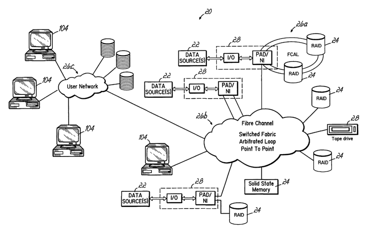
Referring now to the Figures, and to Figure 1 in particular, a real-time data
acquisition and storage network 20 is shown in accordance with the principles
of the present
invention. As will be described in detail below, the real-time data
acquisition and storage
network 20 supports many different configurations for flexible real-time
acquisition and storage
CA 02464771 2004-04-26
WO 03/046735 PCT/US02/38004
-5-
of analog and digital data from one or multiple network-connected data sources
22 to one or
multiple network-connected storage devices 24 during a data recording session,
and precise
reconstruction of the acquired data from one or multiple of the network-
connected storage
devices 24 during a playback session. The data sources 22 do not form part of
the present
invention per se and may comprise any data source typically found in
conventional data
acquisition environments, such as those typically found in launch support,
flight/weapons test,
instrumentation, range telemetry, ASW, ground station, intelligence, telecom
signal capture,
satellite links and telemetry, image acquisition and storage, C41SR, radar,
sonar or any other data
acquisition environment well known to those of ordinary skill in the art.
The real-time data acquisition and storage network 20 of the present invention
is
adapted to provide precise real-time data multiplexing of synchronous signals
and data using
separate files for each data channel stored on a storage device 24, i.e., file-
based real-time
multiplexing by space-time division multiplexing. The real-time data
acquisition and storage
network 20 of the present invention is further adapted to provide precise real-
time data
multiplexing of synchronous signals and data using cell-based data packets
stored and retrieved
across one or multiple networks with transparently connected storage, i.e.,
network-based real-
time multiplexing by space-time division multiplexing. In this way, the real-
time data acquisition
network 20 of the present invention is capable of scaling over a wide range of
individual and
aggregate data bandwidths, number of data input channels, and total storage
capacity, while
preserving precise reconstruction, accurate channel-to-channel time coherency,
and ease of
configuration, monitoring and control.
As used herein, "real-time data acquisition and storage" refers to an
environment
wherein a set of continuous signal streams presented by multiple data channels
are acquired and
stored with essentially no interruption of the signal or loss of the signal
and its data. The signals
from all of the selected data channels are played back with essentially no
interruption of the
signal or loss of the signal and its data and with the precise time
relationship between the
channels that existed during the acquisition.
"Real-time data multiplexing" as used herein refers to an environment wherein
continuous signal streams presented by multiple data channels are acquired and
combined into a
single, ordered or grouped set that can be retrieved, transferred, copied,
deleted, and processed
using a single operation. The combining of these signals maintains the precise
time relationship
between them as they are processed so that essentially no time displacement,
loss, distortion or
change of any signal or its data occurs. The precise time relationship of the
separate channels is
not deteriorated as they are processed.
"Space-time division multiplexing" as used herein refers to an environment
wherein continuous signal streams presented by multiple data channels are
acquired and
combined into a single, ordered or grouped set with sub-elements of the set
separated from each
other and sent to different unrelated locations. The entire set and all of its
sub-elements can be
CA 02464771 2004-04-26
WO 03/046735 PCT/US02/38004
-6-
retrieved, transferred, copied, deleted, and processed using a single
operation. The combining of
these signals maintains the precise time relationship between them as they are
separated to
different locations and processed so that essentially no time displacement,
loss, distortion or
change of any signal or its data occurs. The precise time relationship of the
separate channels is
not deteriorated as they are processed.
Further referring to Figure 1, the real-time data acquisition and storage
network
20 may comprise a fibre channel (FC) point-to-point network, a fibre channel
(FC) arbitrated loop
network or a fibre channel (FC) switched fabric network by way of example. The
fibre channel
network may be configured as a single network or as multiple networks 26a, 26b
and 26c as
shown in Figure 1. The real-time data acquisition and storage network 20 may
comprise SCSI-3
over Fibre Channel Arbitrated Loop for serverless, file-based multiplexing/de-
multiplexing or,
alternatively, ATM over Fiber Channel (AA5) for full ATM cell-based space-time
division
multiplexing as described in detail below, although other alternative network
architectures are
possible as well without departing from the spirit and scope of the present
invention.
In accordance with the principles of the present invention, each data source
22 is
connected to the network 20 through one or more real-time data acquisition
network ("R-T
DAN") modules 28 which provide numerous data acquisition specific functions,
including high-
resolution deterministic time tagging of the input data from Input/output
("I/O") User Interface
cards 30 (see Figure 2), recording precision clock measurement on input and
retrieving clock-
generation data on playback, inputs for auxiliary IRIG time code and voice
track, and
synchronization of multiple inputs/outputs individually and across multiple R-
T DAN modules 28.
One or more storage devices 24, such as RAIDS, optical disks, tape recorders,
solid state
memory or any other conventional storage media, are connected to the real-time
data acquisition
and storage network 20 for storing the data acquired from the data sources 22
through the R-T
DAN modules 28.
In accordance with the principles of the present invention, each R-T DAN
module
28 forms one or more network-connected data acquisition nodes and each storage
device 24
forms a network-connected storage node so that data acquired at any data
acquisition node (i.e.,
R-T DAN module 28) may be applied to the network 20 and stored at any storage
node (i.e.,
storage device 24) during a data recording session. The stored data may be
retrieved from the
storage nodes (i.e., storage devices 24) through the network 20 and routed to
the data
acquisition nodes (i.e., R-T DAN modules 28) for reconstruction of the data
during a playback
session in one embodiment of the present invention as will be described in
detail below.
Real-Time Data Ac4uisition Network ("R-T DAN") Modules
Referring now to Figures 2 and 15, an exemplary real-time data acquisition
network ("R-T DAN") module 28 is shown in accordance with the principles of
the present
invention for interfacing one or more of the data sources 22 to the real-time
data acquisition and
storage network 20. As shown in Figure 2, each R-T DAN module 28 includes one
or multiple
CA 02464771 2004-04-26
WO 03/046735 PCT/US02/38004
Input/output ("I/O") User Interface cards 30 (two shown in Figure 2) which are
selected by type
depending on the format of the data generated by the data sources 22 connected
to the R-T
DAN module 28. For example, each of the I/O User Interface cards 30 may
comprise an Analog
Interface Input/output ("I/O") card 32 (see Figure 51, a Digital Serial
Interface Input/output
("I/O") card 34 (see Figure 6) or a Digital Parallel Interface Input/output
("I/O") card 36 (see
Figure 71 which can be mixed and matched within a single R-T DAN module 28
depending on the
particular data acquisition requirement.
As will be described in detail below, each I/O User Interface card 30 includes
one
or multiple data input channels 38 which are connected to one or multiple data
sources 22 for
receiving either digital or analog data from the data sources 22 during a data
recording session
depending on the I/O card type. Each I/O User Interface card 30 further
includes one or more
data output channels 40 which are connected to one or more of the data sources
22 for applying
either digital or analog data to the data sources during a playback session
depending on the I/O
card type. Clock inputs 42 and clock outputs 44 are also provided on each I/O
User Interface
card 30 as will be described in detail below.
In addition to the various I/O User Interface cards 30, each R-T DAN module 28
includes one or more Packetizer-Depacketizer Network Interface ("PAD/NI")
cards 46 (see
Figures 2 and 4) which are each connected to a respective one of the I/O User
Interface cards 30
in one embodiment of the present invention through a Low Voltage Differential
Signal ("LVDS")
serial data interface 48 and an RS-485 interface 50 as will be described in
detail below. In one
embodiment of the present invention, each PAD/NI card 46 includes a pair of 2
Gbps bi-
directional fibre channel (FC) links 52 for applying data acquired from its
respective I/O User
Interface card 30 to the real-time data acquisition and storage network 20
during a data
recording session and for applying data retrieved through the network 20 from
the storage
devices 24 to its respective I/O User Interface card 30 during a playback
session.
Each R-T DAN module 28 further includes a Time Code Conditioner ("TCC") card
54 (see Figures 2 and 3) which is connected to each I/O User Interface card 30
and each PAD/NI
card 46 within the R-T DAN module 28 through a shared internal bus 56 (see
Figure 2). As will
be described in greater detail below, the TCC card 54 applies timing and
control signals through
the shared internal bus 56 to each of the I/O User Interface cards 30 and
PAD/NI cards 46 to
synchronize and control the I/O User Interface cards 30 and PAD/NI cards 46
within the R-T
DAN module 28 during data recording and playback sessions.
Further referring to Figure 2, each R-T DAN module 28 may include an optional
internal single board Operation, Administration and Maintenance (OAM)
controller 58 which is
connected to the real-time data acquisition and storage network 20 through a
fibre channel PMC
interface 60 and a pair of bi-directional fibre channel (FC) links 62. The OAM
controller 58
communicates with each of the PAD/NI cards 46 through the real-time data
acquisition and
storage network 20. The OAM controller 58 communicates with the TCC card 54
through the
CA 02464771 2004-04-26
WO 03/046735 PCT/US02/38004
_8_
network 20 to a selected one of the PAD/NI cards 46 li.e., PAD/NI Card 2 in
Figure 2), and from
that selected one PAD/NI card 46 through the RS-485 interface 50 which
connects the selected
one PAD/NI card 46 to the TCC card 54. The optional internal OAM controller 58
is operable to
configure, provision, monitor and control the R-T DAN module 28 for a
particular data recording
or playback session. The architecture and operation of the components of the R-
T DAN module
28, including the TCC card 54, the PAD/NI cards 46, and the I/O User Interface
cards 30 are
described in detail below.
Time Code Conditioner ("TCC") Card
Referring now to Figure 3, the architecture of the TCC card 54 is shown in
detail.
The TCC card 54 includes a multiplexer 64 which is capable of receiving a 10
MHz clock signal
from three (3) independent clock sources. These clock sources include an on
board 10 MHz
clock 66, a 10 MHz External Clock Reference 68 or, alternatively, a 10 MHz
clock signal 70
generated by an enabled PAD/NI card 46. The 10 MHz clock signal source is
selected by the
OAM controller 58 from these three (3) independent clock sources through the
RS-485 interface
50 to an FPGA logic controller 72 which controls the multiplexer 64 through a
multiplexer select
control line 74. The 10 MHz clock signal output 76 of the multiplexer 64 of
the TCC card 54 is
applied to each PAD/NI 46 and I/O User Interface card 30 through the 10MHz
Clock Reference
line 78 of the shared internal bus 56 of the R-T DAN module 28. The10MHz clock
signal 76
applied from the TCC card 54 to each of the I/O User Interface cards 30 and
PAD/NI cards 40 on
10MHz Clock Reference line 78 is used to synchronize the I/O User Interface
cards 30 and
PAD/NI cards 46 within an R-T DAN module 28 during data recording and playback
sessions so
that the PAD/NI cards 46 and I/O User Interface cards 30 are synchronized
within 1 clock cycle.
The TCC card 54 includes an IRIG/GPS Timecode input 80 for receiving IRIG
precision timecodes generated from either an IRIG or GPS precision timecode
source (not shown)
connected to the TCC card 54. The IRIG precision timecodes are applied to an
automatic gain
control (AGC) 82 and an anti-aliasing low pass filter 84 before being applied
to all of the PAD/NI
cards 46 and I/O User Interface cards 30 through an IRIG output 85 to the Time
Code
Input/output signal line 86 of the shared internal bus 56 of the R-T DAN
module 28. During
playback, the TCC card 54 is also configured to receive IRIG precision
timecodes at an IRIG input
88 from an enabled PAD/NI card 46 or I/O User Interface card 30 through the
Time Code
Input/output signal line 86 of the shared internal bus 56 of the R-T DAN
module 28. The IRIG
precision timecodes from an enabled PAD/NI card 46 or I/O User Interface card
30 are applied to
a smoothing filter/low pass filter 90 before being applied to an IRIG Timecode
output 92 of the
TCC card 54.
The TCC card 54 also includes an Auxiliary/Voice In 94 which is applied to an
automatic gain control (AGC) 96 and an anti-aliasing low pass filter 98 before
being applied to all
of the PAD/NI cards 46 through the AUX/Voice Output 99 and to the AUX/Voice
Input/output
signal line 100 of the shared internal bus 56 of the R-T DAN module 28. The
TCC card 54 is
CA 02464771 2004-04-26
WO 03/046735 PCT/US02/38004
_g_
also configured to receive auxiliary/voice data during playback at an
Auxiliary/Voice input 101
from an enabled PAD/NI card 46 through the AUX/Voice Input/output signal line
100 of the
shared internal bus 56 of the R-T DAN module 28. The AUX/Voice data is applied
to a
smoothing/low pass filter 101 and then to an AUX/Voice Output 103.
Configuration, provisioning monitoring and control signals from the optional
internal OAM controller 58 are applied to the FPGA controller 72 from a
selected PAD/NI 46
through the RS-485 interface 50 which connects the selected PAD/NI 46 to the
TCC card 54.
Alternatively, if the optional OAM controller 58 is not present in the R-T DAN
module 28, the R-T
DAN module 28 is capable of being configured remotely through the real-time
data acquisition
and storage network 20 from one or multiple remote OAM workstations 104 as
shown in Figure
1.
The TCC card 54 also provides control signals, including a "Real-Time Counter
Stop/Start" signal 106, a "Record Run/Stop" signal 108, and a "Replay
Run/Stop" signal 1 10 to
each of the PAD/NI cards 46 and I/O User Interface cards 30 through the shared
internal bus 56
of the R-T DAN module 28 as shown in Figure 2. The "Real-Time Counter
StoplStart" signal
106, "Record Run/Stop" signal 108, and "Replay Run/Stop" signal 110 are set-up
by the OAM
controller 58 through the RS-485 interface 50 that connects the selected
PAD/NI card 46 to the
TCC card 54. External triggers, including an "External Record Run/Stop" signal
112 and an
"External Replay Run/Stop" signal 114 are connected to the FPGA controller 72
of the TCC card
54 to provide for external triggering of record and replay events. A "Replay
Ready" control
signal output 116 and a "Record Ready" control signal 1 18 are provided by the
TCC card 54 to
indicate that the R-T DAN module 28 is ready and armed for an external
triggering event.
Referring to Figure 15, an exemplary R-T DAN module 28 is shown in detail. The
R-T DAN module 28 includes a rack-mount housing 120 which encloses the TCC
card 54, the
PAD/NI cards 46, the I/O User Interface cards 30 and the internal OAM
controller card 58 which
are connected in the exemplary embodiment of the R-T DAN module 28 as shown in
Figure 2.
The R-T DAN module 28 includes an LCD touch screen 122 to provide for user
inputs to the R-T
DAN module 28, such as the "Record Run/Stop" signal 108 and "Replay Run/Stop"
signal 1 10 to
control record or playback sessions. The LCD touch screen 122 also provides
information to the
user regarding the status of the R-T DAN module 28.
Packetizer-Depacketizer Network Interface ("PAD/NI"1 Card
The PAD/NI card 46 can be selected to record raw data received at the inputs
38
of I/O User Interface card 30. Alternatively the PAD/NI card 46 can be
selected to preprocess
data before recording to either trigger the raw data recording or to directly
record the resultants
of the preprocessing. Examples of preprocessing manipulation include data
compression,
transformations of the data such as FFT, detection of significant data events
and characteristics,
and a multitude of other processing possibilities. In one embodiment of the
PAD/NI card 46, raw
or processed data can be selected for recording. The PAD/NI card 46 can be
selected to
CA 02464771 2004-04-26
WO 03/046735 PCT/US02/38004
-10-
playback raw recorded data stored on storage devices 24. Alternatively, the
PAD/NI card 46 can
be selected to post-process the playback data before presenting it to the I/O
User Interface card
30. Examples of post processing include data decompression, and the selective
playback of
detected events and characteristics.
Referring now to Figure 4, the architecture of an exemplary PAD/NI card 46 is
shown in detail. Each PAD/NI card 46 is interfaced for record and playback of
data to and from
an I/O User Interface card 30 through the Low Voltage Differential Signal
(LVDS) Serializer data
interface 48, such as a National Semiconductor 4838 serializer interface. Each
digital data input
124 of the serializer data interface 48 comprises nine (9) differential pairs
and a clock input
which are generated by an I/O User Interface card 30 which may comprise the
Analog Interface
Input/output ("I/O") card 32 (see Figure 5), the Digital Serial Interface
Input/output ("I/O") 34
card (see Figure 6) or the Digital Parallel Interface Input/output ("I/O") 36
card (see Figure 7)
which are described in detail below. Each digital data output 126 of the
serializer data interface
48 also comprises nine (9) differential pairs and a clock input which are
generated by the PAD/NI
card 46 and applied to the connected I/O User Interface card 30 during a
playback session. In
one embodiment of the present invention, the LVDS serializer interface 48 of
the PAD/NI 46 is
capable of supporting a sustained user data rate of up to about 400 Mbytes/s,
although other
sustained data rates are possible as well without departing from the spirit
and scope of the
present invention.
In one embodiment, the serializer 48 receives and converts the incoming data
from the I/O User Interface card 30 to a 32-bit parallel format that is
applied to a Word Size
Packing Alignment circuit 128. The alignment performed at the Word Size
Packing Alignment
circuit 128 is selectable by the user so that the incoming data from the I/O
User Interface card
is formatted into 64 bit wide words and stored into data FIFO's 130 and 132
through a
25 multiplexer 134. Data stored in data FIFO 130 is available for raw data
recording where every
data byte is recorded just as it is received from the word size packing
alignment circuit 128.
Data stored in data FIFO 132 is available for preprocessing and modification
before being
recorded. Simultaneously with the storage of the data into the data FIFO's 130
and 132, the
precision IRIG timecode signal 85 from the TCC card 54 is applied to a Time
Stamp Decoder and
30 Internal Real Time Counter circuit 136 through an IRIG Time Interface
circuit 138. The Time
Stamp Decoder and Internal Real Time Counter circuit 136 also receives the 10
MHz clock input
signal from the TCC card 54. From the IRIG timecode signal 85 generated by the
TCC card 54,
a time stamp (or time tag) is derived by the Time Stamp Decoder 136. The time
stamp
granularity is correlated to 10 nanoseconds using a high resolution 100 MHz
internal clock
locked to the 10 MHz reference clock. The decoded time stamp is then applied
to time stamp
FIFO's 140 and 142. Each data word of the time stamp data stored in time stamp
FIFO's 140
and 142 represents the time at which each increment of data stored in data
FIFO's 130 and 132
was recorded at the digital data input 124 of the LVDS serial data interface
48. These time
CA 02464771 2004-04-26
WO 03/046735 PCT/US02/38004
- 11 -
stamps are embedded into the data and recorded as a time record of when every
raw or
processed data segment was received by the PAD/NI card 46. The embedding of
time stamps
into the data is described in detail below. The time stamp that is applied to
time stamp FIFO's
140 and 142 by the Time Stamp Decoder and Internal Real Time Counter 136 is a
complete date
time group (DTG) identifying the year, month, day, hour, minute, second, tenth-
second,
hundredth-second, thousandth-second, and ten-thousandth-second. This complete
DTG is
embedded into the data and recorded as a time record of when every raw or
processed data
segment was received by the PAD/NI card 46. The OAM controller 58 initializes
the Real Time
Counter 136 with Year, Month, Day and Time information.
The PAD/NI card 46 is configured for storage of the data on one or more
storage
devices 24 through the 2 Gbps fibre channel (FC) links 52. Data handling
control and
preprocessing or processing manipulation and analysis of the data is performed
by a DSP 144,
such as a TMS320C6204GLW DSP commercially available from Texas Instruments
Corporation.
Other DSPs from the same supplier or other suppliers are possible as well. The
DSP 144 stores
information and/or resultants of data processing to be recorded in a 64K X 64
dual port RAM
146 connected to the DSP controller 144 through a 32 bit, 100 MHz EMIF bus
148. A 512K x
32 FLASH memory 150 and address decode circuit 152 are connected to the DSP
144 through
the 32 bit, 100 MHz EMIF bus 148. The FLASH memory 150 and address decode
circuit 152
contain software programs and control information used by the DSP 144 to
perform its selected
functions. The DSP 144 is connected to the data FIFO 132 and the time stamp
FIFO 142
through the 32 bit, 100 MHz X-Bus 154 supported by the DSP. The DSP 144
controls overall
operation of the PAD/NI 46 using the EMIF Bus 148 and is configured by the
internal OAM
controller 58 or remotely from an OAM workstation 104 (see Figure 1 ) through
the network 20.
The DSP 144 provides the control of data formatting,
packetization/depacketization and,
coordination and monitoring of all functions of the PAD/NI card 46. The DSP
144 also performs
the selected preprocessing and post processing manipulation of the data.
Two (2) compact PCI (cPCI) slots 156 (only one cPCI is shown) are provided in
one embodiment on the PAD/NI card 46. The cPCI slots 156 accommodate lower-
speed 10
devices and peripherals, such as TDM multiplexers (not shown) or multi-channel
converters (not
shownl. Data from low speed 10 devices and peripherals is stored in a 64K x 64
bit dual port
RAM 158 which is connected to the DSP 144 through the 32 bit, 100MHz EMIF bus
148. In
one embodiment, each cPCI slot 156 is capable of maximum burst transfers at
about 133
Mbytes/s, sustained data rates of about 80-100 Mbytes/s when a single slot 156
is used, and
about 80 Mbytes/s aggregate rates when both slots 156 are used. Data can be
simultaneously
acquired from both the LVDS serializer interface 48 and the cPCI slots 156. In
applications
where data is made available simultaneously for recording from the LVDS
serializer 48 and from
the cPCI 156, the DSP 144 programs a PCI Bus Controller 160 to first draw an
interval of data
from data FIFO 130 and write it to a storage device 24, and then draw an
interval of data from
CA 02464771 2004-04-26
WO 03/046735 PCT/US02/38004
-12-
the dual port RAM 158 and write it to a storage device 24. Time stamps taken
from the time
stamp FIFO 140 are embedded into the data from each source data FIFO 130 and
dual port RAM
158. The embedded data format is described in Figure 14. The DSP 144 continues
to issue
write commands alternating the source of the data from data FIFO 130 and dual
port RAM 1 58
throughout a complete recording cycle.
The PAD/NI card 46 includes dual fibre channel (FC) controllers 162 which are
connected to the PCI Bus Controller 160 through a 64 bit, 66 MHz internal PCI
bus 164. Each
of the fibre channel controllers 162 may comprise an ISP 2310 Fiber Channel
Controller
commercially available from Qlogic Corporation, although other fibre channel
controllers are
possible as well. The PCI Bus Controller 160 may comprise a Quick Logic
Programmable Gate
Array QL5064 with built-in PCI Bus Controller commercially available from
QuickLogic
Corporation, although other Programmable Gate Arrays with built-in PCI Bus
Controllers are
possible as well.
In one embodiment of the PAD/NI cards 46, each of the Fibre Channel
Controllers
162 connects in separate 2Gbits/s FC-2 networks and delivers/receives data
across the network
at 200Mbytes/s. The PCI Bus Controller 160 can be programmed in one
application of the
PAD/NI card 46 to simultaneously use both Fibre Channel Controllers 162 and
alternately request
transfers at 400Mbytes/s to/from the data FIFO 130, each Fibre Channel
Controller 162
delivering or receiving 200Mbytes/s across its separate network and achieving
400Mbytes/s
aggregate write or read speed. The Fibre Channel Controllers 162 are assigned
unique addresses
on the network 20 that they are part of so that each PAD/NI card 46 has a
unique network
address associated therewith. Data FIFO 130 and the time stamp FIFO 140 are
connected
through a 64 bit, 100 MHz data bus 166 to the PCI Bus Controller 160 and PCI
Bus Arbitrator
Logic 167. The Fibre Channel Controllers 162 are connected to the DSP 144
through the 64 bit,
100 MHz data bus 166. The 64K x 64 dual port RAM 146 is used to exchange DSP
data
between the 32 bit, 100 MHz EMIF bus 148 and the 64 bit, 100 MHz data bus 166.
The PAD/NI 46 includes multiple synchronization inputs, including the "Record
Run/Stop" signal 108 and the "Replay Run/Stop" signal 110 that connect with
the TCC card 54,
and a "Replay Clock In" signal 168 from the User Interface I/O card 30. The
PAD/NI card 46
also generates a " "Rec RDY" signal 170 and a "Replay RDY" signal 172. These
signals are
used to enable and disable the exchange of data between a PAD/NI card 46 and a
User Interface
I/O card 30, and are part of the controls to synchronize multiple I/O PAD/NI
sets. The "Real
Time Counter Start/Stop" control signal 106 is connected to the TCC card 54
through the
internal shared bus 56 of the R-T DAN module 28.
To synchronize a recording process, a "Real Time Counter Stop" control signal
106 is issued by the OAM controller 58 through the TCC card 54 to all PAD/NI
cards 46 to be
synchronized. The OAM controller 58 resets the Real Time Counter 136 on each
PAD/NI card
46 to the same time value and then simultaneously, via the TCC card 54,
releases the Real Time
CA 02464771 2004-04-26
WO 03/046735 PCT/US02/38004
-13-
Counters 136 on all PAD/NI cards 46 to run using the "Real Time Counter Start"
control signal
106. The OAM 58 issues a record command to each PAD/NI card 46 that identifies
the storage
devices) 24 to use. Each PAD/NI card 46 attaches the storage device 24 and
reads directory
and file information as described below in connection with Figure 14 to
determine the location to
record the data that it is about to receive. Each PAD/NI card 46 seeks to the
selected position
on its attached storage device 24, flushes buffers, and prepares to record.
When each PAD/NI
card 46 is in the record ready state, it enables the 'REC RDY' signal 170.
When the OAM
controller 58 detects the record ready condition of all PAD/NI cards 46, it
issues a "Record
Ready" command to the TCC card 54 followed by a "Record Run" command. The TCC
54
synchronously issues the "Record Run" control signal 108 to all PAD/NI cards
46 and they begin
to fill the data FIFO's 130 and 132 and time stamp FIFO's 140 and 142. The
start time
between all PAD/NI cards 46 is synchronous to within better than 5
nanoseconds. When a
preset data level has filled the data FIFO's 130 and 132, the PCI Bus
Controller 160 detects the
set level and begins to record data and embedded time stamps to the networks)
20 through the
Fibre Channel Controllers 162. The format of how time stamps are embedded with
data is
described in connection with Figure 14 described in detail below. Since
recording on every
PAD/NI card 46 was started synchronously by the TCC card 54, the data being
written by every
PAD/NI card 46 has simultaneously matching embedded time stamps with 10
nanosecond
granularity. The very first byte of data written by each PAD/NI card 46 on its
assigned storage
device 24 was input to the PAD/NI card 46 from the User Interface I/O card 30
at exactly the
same time.
To synchronize a replay process, the OAM controller 58 requests each PAD/NI
card 46 to access the appropriate storage device 24 and seek to the requested
replay data and
begin a read operation. The R-T DAN module 28 can be implemented using a wide
variety of
embodiments to define the requested seek location. In one embodiment, the OAM
controller 58
identifies this position to each PAD/NI card 46 as a Date Time Group time
stamp (DTG). Each
PAD/NI card 46 attaches the identified storage device 24 and reads directory
and file information
to determine the location on the storage device 24 of the DTG time stamp where
the requested
data is stored. The same DTG time stamp is requested of every PAD/NI card 46.
Each PAD/NI
card 46 seeks to the selected position on attached storage, flushes buffers,
and prepares to
receive data from the storage device 24. Each PAD/NI card 46 issues a status
report to the
OAM controller 58 to signal that it is in position. When all PAD/NI cards 46
have responded and
are ready, the OAM controller 58 issues a read command to each of the PAD/NI
cards 46. Data
is transferred by each PAD/NI card 46 from storage to fill the Replay data
FIFO's 173 and 174
which include both data and time stamp data within each Replay data FIFO 173
and 174. When
each PAD/NI card 46 detects that the Replay data FIFO's 173 and 174 are
filled, it is in the
replay ready state and enables the "Replay RDY" signal 172. When the OAM
controller 58
detects the replay ready condition of all PAD/NI cards 46, it issues a "Replay
Ready" command
CA 02464771 2004-04-26
WO 03/046735 PCT/US02/38004
- 14-
to the TCC card 54 followed by a "Replay Run" command. The TCC card 54
synchronously
issues the "Replay Run" control signal 110 to all PAD/NI cards 46 and they
begin to playback
data and other signals such as IRIG In and AUX/Voice In. The replay run start
time between all
PAD/NI cards 46 is synchronous to within better than 5 nanoseconds. Data is
clocked from data
FIFO's 173 and 174 synchronously to this precision by the EXT Replay Clock In
168 from the
User Interface I/O card 30. Time stamps are extracted by a Time Stamp
Extractor 175, and data
is transferred through the LVDS serializer 48 appropriately packed by the Word
Packing
Alignment circuit 128. The first data byte clocked from every PAD/NI card 46
is synchronous to
better than 5 nanoseconds. As data is clocked from the PAD/NI card 46,
requests are made by
the PCI Bus Controller 160 to the Fiber Channel Controllers 162 to read data
from the storage
device 24 and keep the FIFO's 173 and 174 filled.
The PAD/NI card 46 includes an AUX/Voice input/output 176 which is connected
to the DSP 144 through a two channel audio CODEC 177. The CODEC 177 also
receives
precision IRIG timecodes from the IRIG time interface 138. During playback of
AUX/voice data,
the CODEC 177 applies the AUX/voice data to the AUX/Voice input/output 176 and
an IRIG
timecode to an IRIG Replay interface 178.
Analog Interface Input/output ("I/O") Card
Referring now to Figure 5, an exemplary Analog Interface I/O card 32 is shown
in
detail. The Analog Interface I/O card 32 includes an analog input 180, such as
a 70 MHz analog
input, which is applied to an anti-aliasing circuit 182 for conditioning and
filtering of the analog
signal. A bypass 184 is provided through switches 186 and 188 to selectively
bypass the anti-
aliasing circuit 182 if desired by the user. The analog signal received at
analog input 180 is
applied to a 200 MSPS, 10 bit A/D converter 190 which produces the digitized
digital data on
two (2) 10 bit busses 192 and 194, designated the "A" and "B" busses,
respectively. In one
embodiment, the data of the "A" bus 192 is applied to an LVDS serializer 196
which
communicates with a PAD/NI card 46. The data of the "B" bus 194 is applied to
a second LVDS
serializer 198 which communicates with a second PAD/NI card 46. Alternatively,
the "A" and
"B" busses 192, 194 are each applied to one or both of the LVDS serializers
196 and 198 and to
one or both of the PAD/NI cards 46.
A 350 MHz or 200 MHz crystal oscillator 200 is provided on the Analog
Interface
I/O card 32 and is used through External Clock output 201 as the External
Clock In input 202
which is applied to the A/D 190 and the D/A 204. The crystal oscillator 200
also provides an
External Clock Out output 206 which is applied to a second Analog Interface
I/0 card 32 to
provide accurate synchronization of the Analog Interface I/O cards 32. The
Analog Interface I/O
card 32 is free-running and distributes data to the PAD/NI cards) 46 through
the LVDS serial
interfaces 196 and 198. An Encode Sync Out output 208 is applied to a second
Analog
Interface I/O card 32 so that the Analog Interface I/O cards 32 are in phase
with respect to the
"A" bus 196 and "B" bus 198 samples. The Analog Interface I/O card 32 has an
Encode Sync
CA 02464771 2004-04-26
WO 03/046735 PCT/US02/38004
-15-
In input 210 for receiving the Encode Sync Output from a previous Analog
Interface I/O card 32.
The PAD/NI card 46 either stores or discards the incoming analog data under
the control of the
OAM controller 58. The OAM controller 58 selects the width of the data word to
be stored by
the PAD/NI card 46.
During replay of the analog data, the 16 bit 400 MSPS DAC 204 applies a
"Replay Clock Out" signal 212 to the PAD/NI cards 46 (i.e., as EXT Replay
Clock In input 168)
through a data alignment and replay clock 214 during each sample to ensure
that data is
provided to the DAC 204 at the appropriate time from the LVDS serial
interfaces 48 of the
PAD/NI cards 46 and the LVDS serial interfaces 216 and 218 of the Analog
Interface I/O card
32. The data from the PAD/NI cards 46 is applied to a data reclocking and skew
buffer 220
which also receives the replay clock signal from the data alignment and replay
clock 214. In this
way, as data is being clocked out of PAD/NI cards 46 through the replay clock
signal 212, the
data reclocking and skew buffer 220 is applying data to the DAC 204. The
analog data from the
DAC 204 is applied to a phase compensation and smoothing filter circuit 222
and then to the
Analog Signal Out output 224. A bypass 226 is provided through switches 228
and 230 to
selectively bypass the phase compensation and smoothing filter circuit 222 if
desired by the
user.
Digital Serial Interface Inout/Output ("I/O") Card
Referring now to Figure 6, the architecture of the Digital Serial Interface
I/O card
34 is shown in detail. The Digital Serial Interface I/O card 34 includes a
serial input 232 and a
clock input 234. The incoming serial data from the serial channel 232 and
clock 234 are
received through respective ECL-PECL receivers 236 and 238, and then applied
to a serial-to-
parallel converter 240. The clock rate of the incoming serial data is measured
to determine the
serial rate of the data and is stored with the data to be used during playback
to set the playback
data rate. The parallel data is applied to a record data formatter 242 which
stores the data in a
pre-stage data FIFO 244. The record data formatter 242 extracts data from the
pre-stage data
FIFO 244 and adds header information to the data, including the data rate and
how many bits of
that data is valid versus fill. The data and header information are then
stored in a data FIFO 246.
At the same time that the serial data is received, time code data is received
at a
Time Code In input 248 from the timecode channel and AUX data is received at
an AUX IN input
250 from the AUX channel. The time code information is applied to an A/D
converter 252 and
then applied to a time code formatter/deformatter and time stamp circuit 254.
The time code
information is stored in a pre-stage data FIFO 256 and then restored in a data
FIFO 258 with
appropriate header information. The AUX data is applied to an A/D converter
260 and then
applied to an AUX formatter/deformatter 262. The AUX data is stored in a pre-
stage data FIFO
264 and then restored in a data FIFO 266 with appropriate header information.
Each of the data FIFO's 246, 258 and 266 is connected to a data timing/burst
controller 268 through a record data bus 270. The data timing/burst controller
268 extracts
CA 02464771 2004-04-26
WO 03/046735 PCT/US02/38004
- 16-
serial data, timecode data and AUX data from the respective data FIFO's 246,
258 and 266 and
formats that data into packets under the control of the OAM controller 58
through the RS-485
transceiver/receiver 272. The synchronized serial data, timecode data and AUX
data are applied
to the LVDS serial interface of the PAD/NI card 46 during a record session
through an LVDS
serial interface 274 of the Digital Serial Interface I/O card 34. A
microprocessor 276 is
connected to the data timing/burst controller 268 through a microprocessor
systems bus 278
and is responsible for setting up the hardware through hardware registers. To
initialize, control
and monitor the data flow events, the microprocessor 276 is also connected to
each of the
record data formatter 242, reproduce data formatter 280, time code
formatter/deformatter and
time stamp circuit 254 and AUX formatter/deformatter 262 through the
microprocessor systems
bus 278. The OAM controller 58 is able to monitor the Digital Serial Interface
I/O card 34
through the RS-485 link 272 coupled to the microprocessor 276.
During a replay session, the PAD/NI 46 applies data to the Digital Serial
Interface
I/O card 34 through its LVDS serial interface 284. The "EXT Replay Clock In"
input 168 is used
by the PAD/NI card 46 to clock the serial data back to the Digital Interface
I/O Serial card 34.
The data is applied to the data timing/burst controller 268 and then to data
FIFO's 286, 288,
and 290 connected to the reproduce data formatter 280, the time code
formatter/deformatter
and time stamp 254 and AUX formatter/deformatter 262, respectively. The data
timing/burst
controller 268 is connected to the data FIFO's 286, 288 and 290 through a
reproduce data bus
292.
The serial data, timecode data and AUX data are each deformatted and the
header information is removed before the data is stored in respective pre-
stage data FIFO's 294,
296 and 298. The deformatted serial data is applied to a parallel to serial
converter 300 and
serial and clock data are amplified through ECL-PECL receivers 302 and 304 for
replay.
Simultaneously, the deformatted timecode data is applied to digital to analog
converter 306 and
applied to the Timecode Out output 308. Similarly, the deformatted AUX data is
applied to
digital to analog converter 310 and applied to the AUX Out output 312.
Digital Parallel Interface Input/Outout ("I/O") Card
Referring now to Figure 7, the architecture of the Digital Parallel Interface
I/O
card 36 is shown in detail. The Digital Parallel Interface I/O card 36
includes a 32 bit wide
parallel input 312 and a clock input 314. The clock input 314 clocks in the 32
bit wide word of
parallel data to a register 316. The parallel data and clock data from the
register 316 are applied
to the LVDS serial interface 318 of the Digital Parallel Interface I/O card
36. The LVDS serial
interface 318 serializes the data and applies serial data to the LVDS serial
interface 48 of the
PAD/NI card 46. The PAD/NI card 46 accepts the serial data from the serializer
48. Data is
formatted by the PAD/NI card 46 Word Size Packing Alignment circuit 128.
During a replay session, the Digital Parallel Interface I/O card 36 applies a
Playback clock 320 as an external clock input to the "EXT Replay Clock In"
input 168 of the
CA 02464771 2004-04-26
WO 03/046735 PCT/US02/38004
-17-
PAD/NI card 46. In one embodiment of the Digital Parallel Interface I/O card
36 and PAD/NI card
46, this playback clock has a minimum acceptable frequency of 12MHz. The
PAD/NI card 46
applies serial data to the LVDS serial interface 322 of the Digital Parallel
Interface I/O card 36
which converts the serial data into parallel data. The parallel data is
applied to a register from
which it is applied as a 32 bit wide parallel output 326 and clock output 328
of the Digital
Parallel Interface I/O card 36 during replay.
Real-Time Data Acquisition And Storage Network
The real-time data acquisition and storage network 20 of the present invention
is
capable of both file-based real-time multiplexing by space-time division
multiplexing as well as
network-based real-time multiplexing by space-time division multiplexing. In a
file-based
solution, each PAD/NI card 46 serves as its own network controller. Each
PAD/NI card 46
controls the storage device 24 associated with its own files)
storage/retrieval by issuing
commands and data to, and retrieving data from, files on the storage device 24
through the
network 20. In networks 20 having multiple PAD/NI cards 46, each PAD/NI card
46 issues SCSI
commands and data through the network 20 to the destination storage device 24
for the files)
of the PAD/NI card 46. Once provisioned as to file name and destination
storage device 24,
each PAD/NI card 46 controls its own storage resources and file locations on
the storage device
in parallel with other PAD/NI cards 46 on the network 20. The PAD/NI card 46
packetizes data
directly into packets suitable for fibre channel (FC) frames. In one
embodiment of the present
invention, this is SCSI-3 protocol which is a commonly available RAID Fibre
Channel network
interface. Time tagging, clock regeneration, and any other I/O and application
specific
information is placed directly into the framing protocol including file open,
seek, write and read
commands. Figure 14 illustrates an exemplary file structure for storage of
data in a file-based
multiplexed real-time data acquisition and storage network 20.
In one embodiment of the file structure, data is stored on RAID devices in
files as
described by Figure 14. Figure 14 is a logical map to the data stored on the
RAID. "File 1 User
D", "File 2 User D" and through "File n User" represent the File locations
where data is stored.
Each data file is made up of a sequence of Data Frames, "Frame Type 1 ",
"Frame Type 2",
"Frame Type 3" and "Frame Type 4" as shown on Figure 14. Each Frame includes
two fields, a
Data Information Field, and a Data Field. The PAD/NI card 46 writes an 8 byte
Time Tag Word
into the Data Information Field in "Frame 1 " which it reads from the time
stamp FIFO 140. This
represents the precise time with nanosecond level precision that the I/O User
Interface card 30
recorded the first byte of data stored in the data FIFO 130. The PAD/NI card
46 then writes
each data byte to the Data Field of Frame Type 1 that it reads from the data
FIFO 130. The
length of bytes of Frame Types 1-4 is a fixed number. When Frame Type 1 is
filled, the other
three Frame Types are filled with the indicated information and data. The
Information Field of
Frame Type 2 is 64 bytes and is inserted by the PAD/NI card 46 to indicate the
recorded data
rate of the data recorded on I/O User Interface card 30. Frame Type 3
Information is a Frame
CA 02464771 2004-04-26
WO 03/046735 PCT/US02/38004
- 18-
Count number inserted by the PAD/NI card 46 DSP 144 through the dual port RAM
146, and the
Frame Type 4 Information Field contains the Voice Data recorded at the Voice
Input and Output
146 of the PAD/NI card 46. The Voice Data is recorded into the Frame Field by
the DSP 144
through the dual port RAM 146.
The data stored on the RAID is contained in a logical Volume of Files. The OAM
58 instructs the PAD/NI card 46 to "mount" or connect to a storage device 24.
The PAD/NI
card 46 "reads" the Volume File Access Table (FAT) Block shown in Figure 14.
The Volume
FAT is the key the PAD/NI card 46 uses to determine where files are located
and where to write
files that will be stored. The Volume FAT Block includes a Volume Root
Director FAT Block, an
Event FAT Block, a Partition FAT Block, a Directory FAT Block, and a File FAT
Block used to
define the logical hierarchy of files and file locations.
Referring to Figure 8, a file-based network solution according to one
embodiment
of the present invention is shown including three (3) R-T DAN modules 28 to
record and
playback multiple data signals interfaced to a single storage device 24, such
as a RAID, using a
fiber channel arbitrated loop network 332 connecting multiple PAD/NI cards 46.
Each of the
PAD/NI cards 46 of the R-T DAN modules 28 are provisioned or configured from
either the front
panel of the R-T DAN module 28 or from an OAM workstation 334 to issue
commands and data
to, and retrieve data from, the RAID 24 for an aggregate data throughput
limited only by the
network and RAID device. The data of each I/O User Interface card 30 is
packetized with a
measurement of the data frequency and timecode the packet is generated and
written to a
separate file according to the file structure of Figure 14.
Figure 9 illustrates a file-based solution according to another embodiment of
the
present invention. In this embodiment, three (3) separate R-T DAN modules 28
at different
locations are interfaced to three (3) separate storage devices 24 at different
locations using a
fully redundant dual arbitrated loop network 336. A pair of remote OAM
workstations 338 are
connected to the network 336 to provide system-wide provisioning, OAM and
control. Each of
the R-T DAN modules 28 is provisioned or configured as described in detail
above to issue
commands and data to, and retrieve data from, the destination storage devices
24 for an
aggregate data throughput limited only by the network 20 and storage devices
24.
As shown in Figure 10, for even higher scale integration and performance, or
for
systems with data sources and storage devices that are not co-located, switch
fabrics can be
employed, alone or in combination with arbitrated loops. Figure 10 illustrates
multiple R-T DAN
modules 28 and storage devices 24 connected to a switched fabric 340 through
multiple
arbitrated loops and point-to-point links.
In an ATM-cell space-time division multiplexing solution, the PAD/NI card 46
packetizes the data directly into ATM cells for transmission over fibre
channel (FC) frames.
Multiplexed data is stored as a single stream of ATM cells in a single logical
file on the storage
device 24 rather than across multiple logical files.
CA 02464771 2004-04-26
WO 03/046735 PCT/US02/38004
_19_
Figure 1 1 illustrates an ATM-cell configuration of a real-time data
acquisition and
storage network 342 in accordance with an alternative embodiment of the
present invention.
The PAD/NI cards 46 of the RT-DAN modules 28 output ATM cells in either ATM
over FC
(AALS) or ATM over SONET/SDH line interfaces. The ATM switch 344 itself
implements the
space-time division multiplexing/demultiplexing function, routing the ATM to
the appropriate
storage device 24. Following the ATM switch 344, the ATM cell stream is
applied to one or
more processors 346 which serve to perform the "ATM-to-SCSI adaptation" to
package the ATM
data in an appropriate SCSI format for the storage devices 24. The ATM switch
344 performs
multiplexing/demultiplexing functions at the ATM cell level whereas the SCSI
processor
terminates the ATM communications and repackages the stream of ATM cell data
along with the
necessary channel identification and SCSI commands for storage of the data on
the storage
devices 24.
The network architecture of Figure 12 is similar to that of Figure 1 1, where
like
numerals represent like parts, however a fibre channel (FC) switch 348 has
been added to
interconnect the storage devices 24 to the SCSI processors 346.
Synchronization Of Remote
Real-Time Data Acquisition Network ("R-T DAN") Modules
Referring now to Figure 13, synchronization of remote R-T DAN modules 350 and
352 will be described. Unlike the previous embodiments wherein the multiple R-
T DAN modules
46 have been connected to a common network, the R-T DAN modules 350 and 352 of
this
embodiment are geographically spaced apart and there is no means for sharing
timing signals to
the R-T DAN modules 350 and 352 through a common network. In this embodiment,
each R-T
DAN module 350 and 352 include a GPS receiver 354 for receiving precision GPS
timecode
information. The GPS timecode information is applied as an external time of
day (TOD) reference
signal to each of the remote R-T DAN modules 350 and 352. A remote OAM main
control 356
is coupled to each of the R-T DAN modules 350 and 352 through an Ethernet
Control Interface
Wide Area Network 358 to configure, provision, monitor and control the R-T DAN
modules 350
and 352 as described in detail above. Each R-T DAN module 350 and 352 is
programmed with a
record time, and each R-T DAN module 350 and 352 resets its internal counters
and
synchronizes through its 10 MHz reference clock to the GPS timecode
information received from
the GPS receivers 354. At the record time programmed by the OAM Main control
356, the
remote R-T DAN modules 350 and 352 will simultaneously begin recording and
will be
synchronized to each other. A synchronization of I/O signals through
recording, storing and
playback with a precision better than 25 nanoseconds can be achieved using the
methods
described.
The real-time data acquisition and storage network 20 of the present invention
provides significant advantages over known time division multiplexors (TDM's)
used in data
acquisition systems. The powerful and flexible real-time data acquisition and
storage network 20
CA 02464771 2004-04-26
WO 03/046735 PCT/US02/38004
- 20 -
of the present is capable of scaling over a wide range of individual and
aggregate bandwidths,
number of input channels, and total storage capacity, while preserving precise
reconstruction,
accurate channel-to-channel time coherency, and ease of configuration,
monitoring and control.
While the present invention has been illustrated by a description of various
embodiments and while these embodiments have been described in considerable
detail, it is not
the intention of the applicants to restrict or in any way limit the scope of
the appended claims to
such detail. Additional advantages and modifications will readily appear to
those skilled in the
art. The invention in its broader aspects is therefore not limited to the
specific details,
representative apparatus and method, and illustrative example shown and
described. For
example, while the I/0 User Interface cards 30 are shown and described in one
embodiment as
being capable of performing both data acquisition and data reconstruction, it
is contemplated
that the data acquisition and data reconstruction functions may be separated
into two different
cards, with one card being capable of data acquisition only and the other card
being capable of
data reconstruction only. Moreover, while the PAD/NI card 46 has been
described as functioning
with a single I/O User interface card 30 through the LVDS serial interface, it
is contemplated that
multiple I/O User Interface cards 30 may communicate with a single PAD/NI card
46 through a
standard multi-drop signal connection interface. Accordingly, departures may
be made from
such details without departing from the spirit or scope of applicant's general
inventive concept.
Having described the invention, what is claimed is: