Note: Descriptions are shown in the official language in which they were submitted.
CA 02465024 2004-04-19
LOW-LOSS OPTICAL CONNECTOR
FIELD OF THE INVENTION
The present invention relates generally to optical connectors. More
particularly, the
present invention relates to a low-loss optical connector that permits the
alignment and
connection of discrete optical components and arrays, such as waveguides,
fibers and
diode lasers, to other discrete components and arrays, and a method of
fabrication of such
a connector.
BACKGROUND OF THE INVENTION
Improved optical packaging is important for the continued success of photonic
applications in the telecom sector. Recently, there has been a move to Dense
Wavelength
Division Multiplexing (DWDM) technology to meet the demand for increased
bandwidth
for the Internet. The next phase in Internet development will lil~ely focus on
bringing large
bandwidth direct to the home. The modest charge that a homeowner can afford
for such
bandwidth imposes severe restrictions on the cost of any "last mile" system,
including its
components and how the components are optically connected, or wired, to each
other.
When connecting optical components, such as lasers, waveguides and fibers, and
arrays thereof, it is important that the components be precisely aligned to
prevent
transmission losses at the connection, and, in some cases, to preserve a high
degree of
polarization. In order to properly align the optical components, sub-micron
accuracy in
three-dimensions is required.
Numerous manners of aligning and interconnecting optical components have been
used to date. One broad class of connectors uses plugs in one waveguide array
to connect
to sockets in a second array. Such a connector is described, for example, in
U.S. Patent
No. 5,511,138 issued on April 23, 1996 to Lebby et al. In order to obtain
sufficient
alignment accuracy, precision manufacturing that is sensitive to variations in
fiber
diameter and core offset is required. However, even with microfabrication, it
is difficult to
fabricate plugs and sockets with sub-micron accuracy to precisely position
each pair of
waveguides to provide a low-loss connection. This is especially true for large
arrays of
waveguides.
-1-
CA 02465024 2004-04-19
Another common solution for connecting arrays of waveguides, fibers and lasers
to
fibers uses a discrete connector having V-grooves microfabricated into a
silicon substrate.
The connecting fibers are held in the V-grooves such that their ends abut.
Such a solution
is described, for example, in U.S. Patent No. 4,818,058, issued April 4, 1989
to Bonanni.
V-groove fabrication tolerances are very small and the aligmnent is
susceptible to
variations in fiber diameter, core offset and to the effects of contamination
in the V-
grooves. The interconnection of a large number of optical components can
produce
significant stitching error, i.e. accumulation of small errors in waveguide
location leading
to poor overall array alignment.
Presently-employed connectors typically require labor intensive installation,
often
by hand, and do not lend themselves easily to automation, particularly when
connecting
large arrays. There is therefore a need for inexpensive technology to
optically connect
optical and photonic devices such as diode laser arrays, DWDM waveguide arrays
and
fiber arrays. Low cost can be achieved from automation and high product
throughput. It is,
therefore, desirable to provide an improved manner of aligning and connecting
optical
components and for fabricating connectors used in such a solution.
SUMMARY OF THE INVENTION
It is an obj ect of the present invention to obviate or mitigate at least one
disadvantage of previous optical component alignment and connection
arrangements, as
well as manufacturing methods used in relation to such arrangements.
Generally, the present invention provides a method of making connections
between
arrays of optical components such as waveguides, fibers and diode lasers, by
linking them
with optical waveguides written directly in three-dimensional blocks or wafers
of a
transparent dielectric material such as glass. If arrays are to be connected,
any element can
be connected to any other element, providing the flexibility to make cross-
connects. In a
particular embodiment, femtosecond laser dielectric modification is employed
to realize
the connections. An optical connector and an apparatus for making the
connector are also
provided.
In a first aspect, the present invention provides an optical connector for
connecting
an input optical component to an output optical component. The connector
comprises a
three-dimensional optically-transmissive bulk dielectric for abutment with an
input
_2_
CA 02465024 2004-04-19
connection face of the input optical component and an output connection face
of the
output optical component. A connection path is written within the three-
dimensional bulk
dielectric for connecting the input connection face to the output connection
face. The
optical connector is ideally suited for connecting arrays of optical
components, in which
case, a connection path is written within the dielectric for each set of
corresponding
discrete optical components. Multiple optical connectors can be stacked
together to
provide a stacked connector assembly.
In presently preferred embodiments, the three-dimensional bulk dielectric is a
glass
block and the connection path is a waveguide written within the block by
localized
modification of the refractive index of the bulk dielectric, through, for
example,
femtosecond laser dielectric modification. The connection path can be straight
through or
bent. Waveguides can be profiled, such as by widening at certain points, to
minimize
transmission losses at a bend, or to minimize transmission losses at the input
and output
connection faces. Bent waveguides can take numerous forms, such as bent
waveguides,
substantially orthogonal waveguides disposed within the bulk dielectric to
permit total
internal reflection from one of the two waveguides to the other, or
substantially orthogonal
waveguides interconnected by a photonic crystal structure.
In a further aspect, the present invention provides a method of manufacturing
an
optical connector for connecting a first optical component to a second optical
component.
The method comprises locating a first optical connection point, for connection
to the first
optical component, on a first surface of a three-dimensional optically-
transmissive bulk
dielectric workpiece; and writing a connection path within the workpiece from
the first
optical component connection point to a second optical component connection
point, for
connection to the second optical component, on a second surface of the
workpiece.
In presently preferred embodiments, the step of locating includes imaging the
first
optical connection point at an imaging detector, such as by detecting an image
of
maximum brightness and focus at the imaging detector. The step of writing
includes
selectively modifying the refractive index of the workpiece in three
dimensions, and can
include translating the workpiece relative to a writing means. Preferably, the
method uses
femtosecond laser dielectric modification. Multiple connection paths can be
written within
the same workpiece.
-3-
CA 02465024 2004-04-19
In a third aspect, the present invention provides an apparatus for
manufacturing an
optical connector for connecting a first optical component to a second optical
component.
The apparatus comprises means for locating a first optical connection point,
for connection
to the first optical component, on a surface of a three-dimensional optically-
transmissive
bulk dielectric workpiece; and a laser system for modifying the workpiece in
three-
dimensions. The laser system is capable of writing an optical connection path
within the
workpiece for connecting the first optical connection point to a second
optical connection
point on a second surface of the workpiece.
In preferred embodiments, ,the means for locating includes an imaging system
for
detecting an image of the first optical connection point, and the laser system
is a
femtosecond laser dielectric modification system. To permit operation in a
transverse
mode, two orthogonal imaging systems can be used.
In a fourth aspect, the present invention provides a customizable optical
circuit.
This "optical ASIC" comprises a plurality of optical components mounted on a
wafer; and
a plurality of selectively activatable connection paths for selectively
connecting the optical
components to provide a customized optical function. In a presently preferred
embodiment, the plurality of selectively activatable connection paths are
written within
three-dimensional optically-transmissive bulk dielectric blocks abutting
connection faces
of the plurality of optical components.
Other aspects and features of the present invention will become apparent to
those
ordinarily skilled in the art upon review of the following description of
specific
embodiments of the invention in conjunction with the accompanying figures.
BRIEF DESCRIPTION OF THE DRAWINGS
Embodiments of the present invention will now be described, by way of example
only, with reference to the attached Figures, wherein:
Fig. 1 illustrates a first embodiment of a system used to perform a method of
manufacturing an optical connector according to the present invention;
Fig. 2 illustrates a second embodiment of a system used to perform a method of
manufacturing a an optical connector according to the present invention;
Fig. 3 illustrates a third embodiment of a system used to perform a method of
manufacturing an optical connector according to the present invention;
-4-
CA 02465024 2004-04-19
Fig. 4 illustrates a system used to locate a workpiece with respect to a
machining
laser focus according to the present invention;
Fig. 5 illustrates an example of a method of writing bent waveguides in a
transverse mode using a tailored focus in a connector according to the present
invention;
Fig. 6 illustrates an example of a method of writing bent waveguides in a
longitudinal mode by rotating the workpiece, in a connector according to the
present
invention;
Fig. 7 illustrates a fourth embodiment of a system used to perform a method of
manufacturing an optical connector according to the present invention;
Fig. 8 illustrates waveguides bent through 90° using internal
reflection in a
connector according to the present invention;
Fig. 9 illustrates assisting transfer between orthogonal waveguides using
photonic
crystal structures in a connector according to the present invention;
Fig. 10 illustrates connecting waveguide arrays attached to orthogonal faces
of a
single dielectric block in a connector according to the present invention;
Fig. 11 illustrates stacked slabs of femtosecond laser-written waveguides
connecting waveguide arrays in a connector according to the present invention;
Fig. 12 illustrates orthogonal waveguides within a prism according to a
connector
of the present invention;
Fig. 13 illustrates a fixed/fixed configuration of a connector according to
the
present invention with two precision dimension blocks; and
Fig. 14 illustrates a connector according to the present invention using
photonic
crystal structures.
DETAILED DESCRIPTION
Generally, the present invention provides an optical connector for the
connection
of optical components, and arrays thereof. The optical connector is
manufactured of a
transparent or otherwise optically-transmissive material and provides optical
wiring
between optical components to be connected. The optical connector is
essentially a three
dimensional waveguide circuit that is written directly in three-dimensional (3-
D) blocks or
wafers with sub-micron precision. A presently preferred method of manufacture
of such
optical connectors uses Femtosecond Laser Dielectric Modification (FLDM) to
modify the
CA 02465024 2004-04-19
refractive index of a bulk dielectric material on a micron scale with micron
precision in
three dimensions. The present invention applies to any three-dimensional
optical circuit,
and can provide a customizable optical circuit in the optical space, similar
to an ASIC in
the electrical space. Such an "optical ASIC" has a plurality of optical
elements, and a
plurality of selectively activatable connection paths, employing optical
connectors
according to the present invention, for connecting the optical elements to
each other to
provide a customized optical function.
Although embodiments of the present invention will be described herein
primarily
with respect to the interconnection of arrays of optical components, it is to
be understood
that embodiments of the present invention are equally as applicable to the
interconnection
of discrete optical components. The optical components can be manufactured by
any
known technique.
The present invention also provides a general method of making connections
between arrays of optical components such as waveguides, fibers and diode
lasers by
linking them with optical waveguides written directly in 3-D blocks or wafers
of
transparent dielectric materials such as glass to provide the necessary
connection paths. If
arrays are to be connected, any element can be connected to any other,
providing the
flexibility to make cross-connects.
The waveguides can be written by any technique capable of modifying the
refractive index of dielectric materials on a micron scale and with micron
precision in
three dimensions, such as through the use of FLDM. It is known that FLDM can
write
waveguides suitable for light propagation in a number of dielectric materials
without
significant collateral damage. For example, PCT Application No. WO 02/16070 of
Bourne
et al. published on February 28, 2002, which is incorporated herein by
reference, describes
methods to produce waveguides which can operate at A= 1.S~.m.
With the inherent precision of FLDM, it is no longer necessary to manipulate
optical components physically with micron precision. Instead, they can be
brought to abut
a common block of dielectric with no great precision and then connected by
writing a
waveguide between them using FLDM, without a need to physically manipulate the
components to achieve proper alignment. The FLDM laser focus is located with
reference
to the output/inputs of the components to be connected. This process can be
accomplished
using optical techniques and is open to automation.
-6-
CA 02465024 2004-04-19
Waveguides are made in bulk dielectrics using FLDM by moving the focus of the
laser, to which the modification of the refractive index is restricted, within
the workpiece.
The motion can be controlled using computer-linked nanopositioners with high
precision
and the position of the focus in the workpiece can be accurately tracked once
the initial
position is defined. Linear waveguides can be written both longitudinally by
translating
the workpiece along the laser beam axis, and transversely by moving normal to
the laser
beam. A combination of both transverse and longitudinal writing and/or writing
from two
orthogonal directions, as discussed below, is typically used for three-
dimensional (3-D)
structures. The size of the waveguide is adjusted by modifying the size of the
focus, within
restraints imposed by self focussing as described, for example, in the above-
identified
PCT Application No. WO 02/16070, and by rastering the focus to make larger
features.
The use of FLDM permits precise alignment of an FI DM-written waveguide to the
input and output devices, or to other desired locations. FLDM can also provide
sufficiently
bent waveguides for cross-connects and for accommodating designs that require
connections between components on orthogonal faces. FLDM also permits
waveguides to
be written right up to the edges of the block, where input and output devices
axe attached,
without damaging the components or the interface.
In an embodiment of the present invention, the optical properties of the
external
optical elements are used to define their positions and to precisely locate
the connection
points on the surface of a bulk dielectric block. The FLDM beam delivery
optics are used
in reverse to image light supplied by or delivered through the external
optical component
to accurately locate the connecting waveguide to be written in the dielectric
block. The
method of fabrication of the present invention uses many of the concepts
proposed in PCT
Application No. WO 01/54853 to Corkum et al., published on August 2, 2001,
which is
incorporated herein by reference. Corkum et al. discloses femtosecond laser
repair of
micro-defects in quantum well infrared detectors directed by imaging light
emitted from
the defect using the same optical system used to deliver the laser.
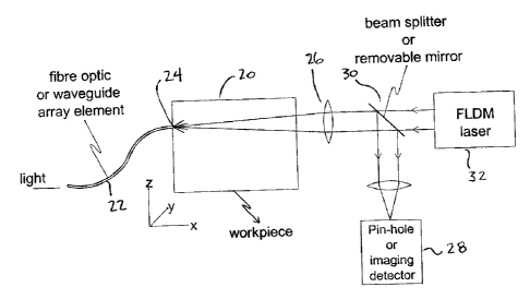
An exemplary apparatus, suitable for longitudinal writing of a waveguide in a
bull
dielectric block workpiece 20 and using a fiber as an example of the external
optical
component 22, is depicted in Figure 1. With reference to Figure 1, y and z
positions of the
connection face 24 where the external optical component 22 is attached to, or
abuts, the
workpiece 20, are found by moving the workpiece 20 relative to the beam
delivery optics
-7_
CA 02465024 2004-04-19
26, or vice versa, to maximize the brightness of the image of the light
emitted by the
external element 22 at an imaging detector 28. The light is provided by an
external source
{not shown) connected to the external optical component. A beam sputter or
removable
mirror 30 can be used to reflect the image to the imaging detector 28. The x
position is
found by bringing this image into focus on the detector 28, the imaging system
having
been previously set up to image the laser focus from the FLDM laser 32. This
can be
achieved by imaging the normal reflection from a planar surface placed at the
laser focus
prior to introducing the workpiece 20. To write a waveguide from the
connection point 24,
the FLDM laser power is activated and the workpiece 20 translated to make a
connecting
waveguide longitudinally through the workpiece to provide an optical
connector. A further
external optical component can then be attached to the opposite end of the
waveguide.
This apparatus of Figure 1 is particularly appropriate for connecting fibers,
waveguides, diode lasers and other optical elements. To align to a diode, the
diode itself
can act as the light source. Although depicted for a single fiber, the
apparatus of Figure 1
is also appropriate for any locating any component in an array of components.
In Figure 1,
the focussing optics 26 axe depicted as simple lenses. The basic idea can be
applied to
more complex beam delivery arrangements and those using reflective optics.
A variation of the apparatus of Figure l, particularly applicable for fibers,
waveguides and other transmissive components, is shown in Figure 2. In the
arrangement
of Figure 2, light from the FLDM laser 32, operated at low power, below the
FLDM
threshold, is collected by the transmissive optical component 34 at the point
or face 24
where it is attached to the workpiece 20. Coupling is optimized when the
relative position
of the workpiece 20 and laser focus is adjusted to maximize the signal
registered by a
detector 36. When maximum coupling is achieved, the FLDM laser focus is
located at the
point of coupling with the external optical component 34. To write a waveguide
from this
point the FLDM laser power is turned up and the workpiece translated with
respect to the
FLDM laser focus to write a connecting waveguide within the workpiece 20, thus
providing an optical connector according to the present invention.
For writing waveguides in the transverse mode, a different approach can used
involving two imaging systems 40 and 42, usually orthogonal, as shown in
Figure 3. The
two orthogonal optical systems are co-aligned to a common focus in the
workpiece 20. A
way of achieving this co-alignment is to image the light emitted from optical
breakdown
_g_
CA 02465024 2004-04-19
caused by the FLDM laser 46 through the other system 42, which includes an
imaging
detector 48. The external component interface point 24, where the external
optical
component SO is abutted to the workpiece 20, is then located using the imaging
system 42
orthogonal to the FLDM arm using the procedure outlined above. Because the
relation of
the FLDM focus to the imaging system focus is previously determined, the FLDM
focus
can then be positioned anywhere with respect to the external optic to write a
waveguide in
the dielectric block to provide the desired connection path. Focus adjustment
can be
provided by adjusting the position of the beam delivery optics 52.
Writing from two orthogonal directions is complicated due to the dielectric
block
worlcpiece 20 having a refractive index greater than its surroundings. With
the focus inside
the workpiece 20, the effective focal length of each beam delivery lens 52 is
dependent on
the distance of the lens from the workpiece. If the foci are co-aligned in air
to calibrate
their relative positions, correction will have to be applied depending on the
distance
between the surface of the workpiece 20 and the focus. This distance can be
known with
sufficient accuracy if the dimensions and position of the block are pre-
determined or
measured in situ.
An algorithm to compensate for the position dependence of the focal length can
be
based on standard optical formulae. It is also possible to co-align the foci
by observing
FLDM laser-induced breakdown in the workpiece 20 itself by operating the FLDM
laser
46 at high power. This can be done at some location where damage is not
important. The
correction will then be small if the alignment is made close to where the
waveguide is to
be written. An alternative technical solution is to immerse the workpiece in
index
matching fluid.
Certain applications do not require writing connection paths to pre-connected
components. For instance it is effective, in certain cases, to 'write
connecting waveguides
in a block so that their inputs and outputs match precisely the known
configurations of
external arrays {e.g. photodiodes or diode lasers). A single physical
alignment step can
then be used to align the whole array. In this case, where there is no
external component to
which to directly align, the workpiece ZO can be located precisely with
respect to the laser
focus by operating the FLDM laser 54 at low power, below the FLDM threshold,
and
observing the light reflected from surfaces of the workpiece block 20, as
depicted in
Figure 4. The optical system is set up so that when the laser focus is at a
surface of the
_g_
CA 02465024 2004-04-19
workpiece 20 its reflection is in focus at a detector 56. If the dimensions of
the block 20
are known, and the block faces are orthogonal and parallel, measurements from
three
orthogonal surfaces locate the block precisely. Rotational motion of the
workpiece 20 is
required for this procedure in addition to x,y,z, translation. If the
dimensions are not
known, measurements from further surfaces can be made until the position and
shape of
the block are determined.
There is also a difficulty in writing a waveguide right to the end of a
dielectric
block where waveguide arrays may be butted and epoxied. The laser damage
thresholds at
the glass/air interface or the glass/epoxy interface are much lower than that
of the bulk
material and damage can occur at these surfaces. To avoid damage at the
interface, the
waveguides can be written as close to the interface as possible without
causing damage.
This leaves a short free propagation space between the external component and
the
internal waveguide. However, for many applications such losses may be
acceptable.
Alternately, the position of the external optical component in the butted
position
can first be accurately located with an imaging system, as described above,
and can the
external component can then be pulled back, in the range of SO~,m, until the
laser has
written the desired internal waveguides. The external component can then be
moved back
into position for permanent connection. Index matching fluids or the use of a
temporary
bonded dielectric layer can be used to prevent damage to the glass block as
outlined, for
example, in Bourne et al.
Another method of avoiding damage at the interface uses a precision dimension
block. All the external components in an array are located relative to
reference positions
on the block. Waveguides can then be written in the block to the recorded
positions with
the external components completely removed. Replacing them requires a single
physical
alignment. If surface damage occurs this approach also gives the option of
polishing any
damaged regions.
Where coupling conditions permit, the waveguides forming the connection paths
can be reverse tapered to increase in diameter as they approach a surface of
the block. A
wider waveguide requires a lower change in refractive index, which can be
achieved with
lower laser dosage, decreasing the extent of surface damage.
A particular advantage of the present invention is the ability to write
connection
paths with bends directly into a dielectric block. The volume element modified
by FLDM
-10-
CA 02465024 2004-04-19
without motion of the workpiece is determined by the focal parameters and non-
linear
absorption as described, for example, in Bourne et al. Using spherical optics
the active
volume is relatively long and thin and can be quite small, typically a 15~.m x
2~txn
ellipsoid for f3.6 optics. Bourne et al., for example, describes strategies
for writing
waveguides with circular cross-sections despite this asymmetry. These
strategies include
rastering, writing longitudinally and use of combined cylindrical/spherical
optics to tailor
the laser focus. Connectors of the type described herein can require
waveguides bent as
much as 90° or more. Writing such bent connecting waveguides with a
long thin activated
volume can be met by several complementary strategies.
One such strategy, using cylindrical/spherical beam delivery optics 60, such
as
described in Bourne et al., and adjusting the cylindrical element 62 during
writing to rotate
the laser footprint 64 to keep it tangential to the resulting connecting
waveguide 66, is
shown in Figure Sa. Figure Sb shows a top view of the workpiece 20 with the
resulting
waveguide 66. A second strategy for producing a bent waveguide 68 in a
workpiece 20
involves writing the waveguide longitudinally while rotating the workpiece 20,
as shown
in Figure 6.
Another method and apparatus for writing a bent waveguide connector uses high
f
optics to reduce the length of the active volume to below the waveguide
dimensions and
write the waveguide from one side, starting in the longitudinal mode and
moving to the
translational mode, or vice versa. Rastering a small active volume compared to
the
dimensions of the waveguide allows the refractive index profile of the
waveguide to be
tailored by controlling the exposure. Asymmetric profiles are achievable and,
in particular,
it is possible to deepen the refractive index change on the inside of
waveguide bends to
reduce losses and thereby decrease the radius of the bends.
Similarly, high f optics can be used to reduce the length of the active volume
to
below the waveguide dimensions and write the waveguide from two orthogonal
sides,
either longitudinally or transversely, as suits best to obtain the specified
waveguide
profile, again using rastering to define the waveguide dimensions. This can be
achieved
using a variation of the optical arrangement shown in Figure 3. Beam sputters
and/or
removable mirrors 70 are used to exchange the laser delivery 72 and imaging
arms 74 of
the system, as depicted in Figure 7, and allow laser beam delivery from either
direction, or
even both directions, while still knowing the position of the foci. Image
detectors 76 and
-11-
CA 02465024 2004-04-19
78, in conjunction with adjustable beam delivery optics 80 and 82, permit
accurate
positioning and locating of the beams. The arrangement of Figure 7 is
especially useful in
writing waveguides connecting an external component 84 to an external
component
situated on an orthogonal surface of the block 20, as swapping the imaging and
laser
delivery arms allows both optical components to be located with precision.
Another method of bending light within the workpiece 20 is shown in Figure 8.
Internal reflections at a surface 86 can be used to transfer light between
angled linear
waveguides 88 and 90. In order to avoid surface damage problems at the
90° bend, a
temporary bond can be made to a prism so that the waveguides 88 and 90 can be
written
all the way through the interface. Alternatively, the waveguides 88 and 90 can
be written
to cross just below the angled surface 86 that can be polished down
subsequently. The use
of total internal reflection in a prism, that essentially acts like a turning
mirror, results in a
considerably lower effective bend radius. This not only allows compact
connectors to be
made but also reduces the optical path length of the FLDM written waveguides.
The short
length of the waveguides (<1 cm) can result in a reasonable overall connector
loss despite
the waveguide loss per cm potentially being considered too high for telecom
applications
(e.g.> 0.2 dB/cm).
Rather than relying on total internal reflection to provide a tight bend,
photonic
crystal structures 92 can be used to assist in guiding light around tight
bends and linking
two waveguides 94 and 96 written in the workpiece 20, as shown in Figure 9.
These
structures 92 can be written by a combination of FLD1VI and chemical etching
as
described, for example, in U.S. Publication No. 2003/0235385 to Taylor et al.
published
December 25, 2003, which is incorporated herein by reference.
The methods and connectors of the present invention can be used in any number
of
configurations. For example, straight through connections can be made in a
block of
dielectric to reference waveguide locations. As described above, techniques
for forming
straight through connections require clear line of sight through the opposite
face. Straight
through connections cannot be made if both the input and output external
arrays are in
position. To overcome this limitation, an array of external input components
can be placed
in contact but not attached to a block face. The location of the array is then
referenced
with respect to the block face. Optical procedures described above can be used
to locate
individual waveguides and record their position relative to reference
positions on the
-12-
CA 02465024 2004-04-19
precision block face. A set of output components can then be butted to the
opposite face of
the block where the locations of all the output guides can be obtaived, again
referenced to
the precise dimensions of the block. Precision rotation of the block through
180° keeps the
previous reference positions known. Waveguide connectors can then be written
in the
block according to the recorded locations of the external waveguides. In
principle the
block can be polished to remove any surface damage; then, the external guides
can once
again be brought into contact with the appropriate faces of the block, aligned
and glued
into position.
In a variation of the straight through configuration, optical conditioning
elements
can be inserted between waveguide arrays or demountable connections can be
made
between arrays. The block, with the straight through written waveguides, is
cut in half at
right angles to the written waveguides and polished on its two inside
surfaces. The
external arrays are then connected to the outside halves of the block and a
gap is left
between the blocks to insert an optical element such as a filter. This
configuration is
important since its function, whereby light delivered from one fiber passes
through an
optical element where it is modified then collected by another fiber, is a
common
requirement in telecom photonics. This requirement is currently met using
discrete
components assembled from fibers, where thermally expanded core technology is
used to
create fiber tapers that permit greater light collimation through the optical
element. Using
the connector of the present invention, raster scanning or focal spot
modification can be
used on-the-fly to control the waveguides diameters to adiabatically expand
them to
produce a collimated beam through the optical element where it can be received
by a
similar expanded waveguide in the second block which then connects to an
external
waveguide. If the intermediate element is left out and mechanical provision is
made to
bring the two parts together with repeatable precision a demountable array
connector
results.
A further configuration permits optical connection of attached waveguide
arrays to
attached waveguide arrays in a single block of dielectric. In this
configuration, shown in
Figure 10, arrays of optical components 100 are attached to one block face 102
and
connected by internal waveguides 104 to other arrays 106 on an orthogonal
block face
108. The arrays are attached to orthogonal faces since it would be very
difficult for the
imaging system to locate the guides if they Were on opposing faces and be able
to deliver
-13-
CA 02465024 2004-04-19
femtosecond laser light to connect them without the attached guides blocking
the laser
beam. Methods for writing such bent waveguides 104 are given above. FLDM
writing of
waveguides is not restricted to blocks of dielectric material but can include
other
geometries such as slabs 110 which can be stacked as shown in Figure 11.
A variation of the bent waveguide configuration uses a prism 112 instead of a
block as shown in Figure 12. The prism angle is chosen to provide efficient
total internal
reflection of the guided light to form a bend 114 of about 90°. In
order to avoid surface
damage problems at the 90° bend, it can be advantageous to make a
temporary bond
between two prisms and write the waveguides all the way through the interface
of the
prisms.
To provide a connection of attached waveguide arrays to attached waveguide
arrays using two precision dimensioned blocks of dielectric 116 and 118, the
configuration
of Figure 13 can be used. Waveguide, fiber or diode laser arrays can be
attached to one
face of each block. Femtosecond laser written waveguides 120 are fabricated
from each
external guide to a predetermined (i.e. referenced) location on the opposite
face of each
block. The reference locations can be determined using the sharp edges of the
block faces
together with the precise dimensions of the block. The blocks are then aligned
and joined
to produce array to array optical connection. This approach does not require
the use of
bent waveguides or the need for two focussing systems. The waveguides can be
expanded
at the block/block interface to allow for alignment inaccuracies between the
two block
faces.
Figure 14 shows a configuration using photonic crystal structures to assist in
guiding light around tight bends. This example demonstrates how photonic
crystal
structures 122 can be used to assist light guiding around tight bends in the
plane of an
accessible surface. After the photonic crystal structures 122 have been
etched; external
components 124 can be attached to the blocks and internal waveguides 126 can
be written
from them (as shown in Figure 10) to just enter the photonic crystal bend
zone, thereby
completing the optical connection. Multiple photonic crystal arrays can be
written on the
top of the block to provide complicated bending and light redirection
functions. The use of
photonic crystal technology to dispense with large 4 mm radius bends can
shrink the size
of the optical connector signif cantly, and also lowers the connector loss.
-14-
CA 02465024 2004-04-19
Increased value can be achieved by incozporating components such as splitters,
couplers, mode converters, adiabatic tapers etc. into the block dielectric
connector, along
with the basic waveguides for optical connection.
A further application of the optical connectors and connection method of the
present invention using FLDM, permits any number of waveguides to be written
internally
in connection blocks. Such waveguides can be pre-fabricated by prior FLDM or
other
microfabrication techniques. In this manner, the optical equivalent of an
Application
Specific Integrated Circuit (ASIC) used in electronics, where customized
(application
specific) function is realized by making or breaking links between arrays of
standard
components provided on the mass-produced ASIC chip, can be provided. In the
optical
ASIC, as is provided according to an embodiment of the present invention, FLDM
is used
to make the connections between pre-existing optical components on a chip. In
this
respect, the optical ASIC is an inverse analogue of electronic ASICs where
current is
directed by removing links. Connecting the components involves selectively
writing
waveguides within the provided dielectric connecting blocks, or writing
couplers to
connect the pre-existing waveguides to the desired components. As in its
electronic
counterpart, the optical ASIC ca~z be generic and produced with high volume
economy.
The present invention, in its various embodiments can provide a number of
advantages and/or novel features. It permits the use of a single dielectric
block with
directly written waveguides to connect optical components together with sub-
micron
precision. The invention permits the application of FLDM to make these optical
interconnects. The use of two coupled orthogonal optical systems permits
location of the
waveguides as well as delivery of the femtosecond laser radiation to write the
internal
waveguides to connect external arrays of attached waveguides. The use of
optical
techniques takes advantage of the optical properties of the components to be
connected, to
direct FLDM waveguide fabrication with the precision necessary to make low-
loss
connectors. The invention also permits the creation of a 3-D optical ASIC
using FLDM as
an enabling technology for its realization. Precise control, with respect to
spatial and depth
of refractive change, afforded by FLDM permits waveguide profiles to be
tailored, thereby
improving propagation of light through bent waveguides. The invention also
permits the
use of two precision dimension blocks to permit optical wiring between arrays
of
waveguides permanently attached to opposing block faces. The invention also
permits the
-15-
CA 02465024 2004-04-19
use of total internal reflection from the inside face of a prism as a means of
guiding light
around a 90° bend and making a compact connector.
The above-described embodiments of the present invention are intended to be
examples only. Alterations, modifications and variations may be effected to
the particular
embodiments by those of skill in the art without departing from the scope of
the invention,
which is defined solely by the claims appended hereto.
-16-