Note: Descriptions are shown in the official language in which they were submitted.
'~;E~SCPAI~I
.~.:. :; ~r,~ ,~ :~a~ ~~ ::~,;a
_ . _ .__ - 1
OPTICAL DISPLACEMENT SENSOR
This invention relates to an optical displacement sensor
element, e.g. for use in a pressure sensor or a microphone,
comprising two flat surfaces being separated by a cavity
defined by a spacer, the distance between the surfaces being
variable depending on pressure fluctuation in the environment
relative to the pressure~in the cavity.
Until recently displacement sensors such as microphones
has been based on capacitor structures and impedance
measurements. This has a number of disadvantages related to '
sensitivity, high voltage biasing, isolation between layers,
alignment and positioning of membrane relatively to back
electrode, high requirements to preamplifiers, and non-linear
response, all resulting in costly and complicated solutions.
Optical displacement sensors are able to solve many of
the major problems that capacitive sensors are suffering
from. There are no problems with biasing or need of
electrical isolation. Interferome~tric sensors are able to
achieve equal or better sensitivity than capacitive
displacement sensors with less demanding electronics, but
until now these solutions have been relatively expensive
because the problem with alignment and positioning has not
been solved.
Optical displacement sensors are described in a number
of publications, such as Nikolai Bilaniuk:, "Optical
Microphone Transduction Techniques" in Applied Acoustics,
vol. 50, No. 1, pp 35-63, 1997, Dennis S. Greywall:
"Micromachined optical-interference microphone", in Sensors
and Actuators 75 (1999 257-268, and David Keating: "Optical
Microphones" in Microphone Engineering edited by Michael.
Gayford, Oxford Boston Focal Press 1994. These publications
describe a number of different types of optical microphones,
and among these, solutions based on Fabry-Perot
interferometers.
..y.f:;...,g-. rry:,;i~p..~i .r;;~-......~:m
..,..:::.4'~ e...i.~..' ~."%':7~:.. ~ u,.. ~Z~ .
.. ,k....v: F .~i.) ._
y~.'..:v\:~.'.~r'<5. -.:, i-;<,:~,.r . i .
.::::.\.~ EE:,,
<~e, '~:u'f4» .:.
':~~::.::.:r
a'e~",:V
f i>y CA 02465311 2004-04-29 ~.~~,~ ~,r~"~~r,"Q~ 1 ~ 'fix--' ,~'~%
;~::~.,~;;.; ,....~~",. ,s,. ..;.. ..._~~,.. .~._~..:.a
~;x .s ,.".,..,...,.,;~;.:a;~"~:a~::,.i<;.,e.<:,:,,<;;;,a~~:~:.«<:::
~i rt
~~ Pr~~n~~d ~ ~6'~;~,1'~~~?~C~3
tar, ~~' d E .,.~'~1~' -..a'r~4 ~ ,.~~~ w-fra
nn~.~ f~v.... ~,.. ,.
2
Other Fabry-Perot sensors are described in US patent
5,909,.280, US patent,5,128,537 and international patent
application WO 87/02470
US 5,909,280 describes a spectrometer comprising a
detector integrated in a silicon substrate underneath one of
the Fabry-Perot mirrors, while the second mirror is mounted
on a spring structure. The distance between the mirrors, are
adjusted electrostatically. The light to be interrogated is
provided through an optical waveguide.
US 5,128,537 and WO 87/02470 shows Fabry-Perots,
pressure sensor and interferometers, respectively, with
external detectors and light sources.
CH 681,047 A5 describes a measuring system, especially
for pressure measurements, comprising two Fabry-Perot
interferometers of.which the first is coupled to a cavity in
which the pressure is to be measured, as well as a light
source and an optical fibre for transferring the output from
first to the second Fabry-Perot interferometer. The.
reflecting surfaces in the second interferometer being
positioned in a transparent material and a silicon material,
respectively, said silicon material also being provided with
a detector. This is a complicated and thus fairly expensive
solution. Also, as the optical wave fronts transferred from
the optical fibre will be spherical, interference will arise
on the detector surface limiting the sensitivity. It is an
additional object of this invention to provide a simple and
cost efficient solution having high sensitivity.
Microphones based on Fabry-Perot interferometers are in
general difficult to align, as optics must be aligned
correctly relative to the interferometer, and the two
surfaces forming the Fabry-Perot cavity must be parallel
relative to each other. This problem is mentioned in
Keating's article but only as a minor problem, as other
problems related to other microphone types are deemed to be
more difficult to handle than the problems related to the ,
Fabry-Perot interferometer.
4u ?",~.
CA 02465311 2004-04-29
.~ s
3
The need for high precision alignment of the cavity
' reduces the possibilities for making low-cost microphones
which are able to compete with ordinary microphones.
The alignment probTems.are used as an advantageous
feature in the microphone described in US 6.055,080. This
solution is, however, still a complicated and expensive .
solution. It is an object of this invention to provide a
optical sensor element and device which reduces the above
_ mentioned alignment problems by implementing the detector in
one of the Fabry-Perot surfaces in addition to exploiting the
inherent alignment of the wafer bonding process.
It is also an object of this invention to improve the
solution disclosed in the above mentioned article by
providing an optical sensor element for measurement of
pressure fluctuations, acoustic signals or the like without
requiring individual alignment of optics or complicated
electronic circuits. It is also easy to manufacture in large
quantities without need for costly precision alignments of
any optical parts.
These objects are obtained with a sensor element and-
device as described above being wherein both of said surfaces
are at least partially reflective, and said first surface
being provided with at least one optical detecto-r, and said
second surface being provided on an at least partially
transparent material, the sensor also comprising an
essentially monochromatic and essentially point shaped light
source directed toward said parts. and means for providing
inphase addition of the emitted light on the surface_~of said
at least one detector.
The phrase "inphase addition" here refers to
interference on the surface of the sensor either provided by
collimating an essentially coherent wavefront so ws to cause
any level of constructive or~destructive interference on the
whole detector surface, or by providing a ring shaped
detector. A point shaped source emitting essentially
CA 02465311 2004-04-29
~p,.l:x~;f.~ >~::):::.:,A"A.~.:~.:.x.::C~~A~2.~.i3::;:'\\:~.::
x,::<,e~y , ..::. ~.~;~za2:~~,.i::::.i:D".:: >:::.::~: a.:v.~.:..
W a L '3: ..., :,~"..~"' k
'.; H 4. . ~,::' ~. ~~. , ' : ~:;..:~ 'a:::':: " >:..:
p=,.~r .;~. ~\~S;:c::; ".:.:\~:.:>.. :: '.~.5:~':.::;'. ..
:'iT:.~\...,~:::.: ,..s~:?
.;'...-:;:3 ..a,.,'w'.v~:L,:,~...,»...W »a.~.%::);i~:y"'~y,;~">.i::i<
::.:.vs':~k..s",.
~~ oo~ob~~
_.~;~ h~,n~.,~ ~ ~r~.~~ .~,~u~:~
4
coherent, spherical wavefronts will result in a circular
- . interference pattern the detector, thus inphase addition on
the detectors is provided by number of concentric ring shaped
detectors.
More specific, the invention is characterized as
presented in. the accompanying independent claims.
The invention will be described in more detail below,
referring to the accompanying drawings illustrating the
invention by way of example. It is further characterised as
stated in the accompanying claims.
Figure 1 illustrates a simplified Fabry-Perot interferometer
Figure 2 illustrates the transmitted intensity T on the ,
optical axis of the sensor for different values of
the finesse F as a function of the cavity distance
d.
Figure 3 illustrates the cross section of a sensor according
to the invention.
Figure 4 illustrates an alternative embodiment of the
sensor.
Figure 5 illustrates schematically another alternative
embodiment of the sensor together with the .
calculated transmitted intensity T for three
different cavity distances (10~,, 10~.+~,/8, 10~,+~./4)
as function of angle of incidence 8.
Figure 6 illustrates an example of a detector being
constituted by a number of concentric detector
rings.
Figure 7 illustrates detector and four through holes.. for
controlling the squeeze-film effect.
Figure 8 -illustrates an embodiment of the invention using a
force feedback control of the position of the
surfaces according to the invention.
The Fabry-Perot interferometer's elements are
illustrated in Figure 1. It comprises two flat parallel
.::...:.>>:::<<> :<:"::>->,::;,,~.~>:: .,.~;~.
.::.~~k,:;:::.A,... ~/tn;>~:...~.:;
.p::2p~f :..~J,.., .
y'F,'~:.....:.,!.y:.::.:.,E'_y~..'~;:,.....s... ~::.::~:"~~~,~~;,_~
~ .. ::.... . : .:..,':...... :..
! ~.~ : '~' :...:
~~'il~, .....', :.": :: ::.'.
~. :~~'::"~i~w. ..s. ...... :~'~~'.
~'.:;a::rte;:;2:
CA 02465311 2004-04-29 .A,~'u~,,~.".,.
:.:;<:..a.<~.~<:'s:,..,:r:>,::.,
~f'y'F :......,.; "."::.....aaa; ...w::;\ui:'.:
S,'t~:~,'~'':,.:ic>>:~, u..,..:COa..,y,...
- 5
surfaces (1 and 2), often coated to obtain a chosen
' reflectivity,~separated by a spacer~distance d to form a
cavity. A sufficiently monochrome and coherent collimated
. light source (6) is-directed towards the cavity, and the
transmitted light through the cavity is collected by a
detector (not shown). When the cavity distance varies, the
transmitted light intensity varies due to constructive and
destructive interference between the cavity surfaces. The
intensity on a detector positioned on the opposite side from
the light source varies according to
T=Tmax/ (I+ (2F/~t) 2si.n2 (2~td/~,) ) 1
where F is the interferometer's finesse, a measure of
the reflectivity of the. cavity surfaces, and ~, is the optical
wavelength (Born & Wolf "Principles of optics,
electromagnetic theory of propagation, interference and
diffraction of light"). If the finesse equals one (low
reflectivity surfaces), the optimal cavity distance is
d = ,~,/8 + m~,/4 + n~, ; m, n=0, 1, 2,...
where the greatest linearity is obtained.- If the finesse
increases, the optimal distance is
d = m~./2 _+ d ; , m=0,1, 2, ..., .d E 0 . . ~,/$
D is close to or may be essentially equal to max(/a(T)/d(d)/)
where T is the transmitted intensity as defined in equation 1
and d is the cavity distance. Figure 2 shows the transmitted
intensity as function of cavity distance in the range ~, to
2~,, for finesse = 1, 10 and 100.
1~..:~~ CA 02465311 2004-04-29
.a
~ ~.~s~
'; ~ i(s' f ~.i cs'G I ~' y~ i (u f~ ~e ,~~R ((~~''~~
f' ~~~~~~~iyi~~~ ~~ ~i~' ~ ~ tt~~~~ i ~~~
~~,.~~st!'~.x~c'..~~i.sr..,:,t'~.rw~u:..,~~.?;~e!~-~,.~,aza~.:.~.ud~~.
au~"~,ls,~~~t
6
The present invention is based on the Fabry-Perot.
interferometer and reduces the above mentioned alignment
problems by implementing the detector in one of the Fabry-
Perot surfaces in addition to exploiting the inherent
alignment of the wafer bonding process. A preferred
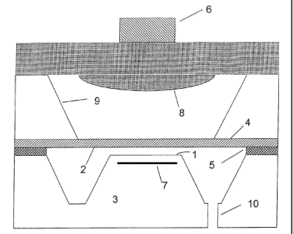
embodiment of the invention is illustrated in Figure 3. The
first sensor element part 3 is preferably made from silicon
and pn junctions constitutes the detector or detectors 7. The
techniques for making this type of detectors are well known
and will not be described in any detail here. One or more
holes 10 may be used to secure pressure equilibrium in
applications like a microphone. The Fabry-Perot cavity's.
first surface 1 is the detector surface. The second surface 2
is made of a partially reflecting flexible and transparent
material 4, for example silicon nitride, and is secured on a
rigid frame 9, made of for example silicon.
According to a preferred embodiment of the invention the
detector 7 is provided with a large surface area, thus
reducing the need for exact alignment of the sensor.
A spacer 5 defines a cavity between the surfaces 1,2 and
separates the two element parts 3,4. The spacer may be a
separate part or be constituted by a part of the first or
second element parts.
Also illustrated in Figure 3 is a point shaped light
source 6, e.g. a light emitting diode (LED) or a laser, and a
lens 8, e.g. a moulded plastic lens, for collimating the
light. The light source and the lens are fastened on the
rigid frame 9 thus maintaining a predetermined distance
between the lens and the Fabry-Perot interferometer. The
light from the source 6 is collimated by the lens 8 to
provide a plane wavefront through the Fabry-Perot to the
detector. Thus the interference conditions will be
essentially equal over the whole detector surface resulting
in a measured intensity being a sum over the whole detector
7. '
~~.n, z_r~
~:~;a:>,.~,<,r> i
:~:.::~".~.>:
a,:: ~y--.;
.~.:~~..<..::, a.,_..:.:
~,":.~.:~.,.."Y ~.,:.~,..,,
..>;~:.:,:.:,..~.:.<,:~~>.: ~::..~,.:..".. , .n ~ ~~:ss ,. , , ~
.n,..K..;.
r_~
~~f ,~ ; :x . ~,
z~ .~.% :"
,~i,' ,'"i
.. :)' : ::.
x: .: ';?':.: ~.:~:.,.::~~::,',~~,.y ._.,1 ." ~.
.. vP~.-~ '~
CA 02465311 2004-04-29 ~:~~~~'..:..,~:~..~
~....y...~.;::...~,.~....:.~;,~~:yw::::...~.a is..,.",s;;:,.~. ,<"..:~:..,
._.~.ssa~..;::~ . :~,43..r°., ~~, .
d:.::~? as.""~t;.d,ai~~a=~~.'.!a:: ez:...~r: .i
:,:-~~~x,:i~at~<:~;,i;.ri,>~xk:<:we:;::,~;xrs:":«:.,;
isu s
ar ~~ ~t ~ ~' ~R~y t ,~~ffi
~~P~i~i~ec~~ k(3~6'~1~~F# COQ
~i :rS: r . ' ...:,.. s. . ...,.~, ~ "c s, ~.. ~ ....a..3.:>.
7
In another embodiment of the invention, illustrated in
' Figure 4, the pn junction 7 is implemented in the membrane
itself 4. The lower element part 3 may be made of silicon and
the detector may be integrated in a thin silicon membrane.
The upper element part 9 is made of a transmitting material
- e.g.,pyrex, and the partly reflecting and transmitting
surface 2 may be coated to obtain higher reflectivity.
According to another embodiment of the invention the
detector is positioned on the transparent element part, e.g.
by making the transparent part and detector sufficiently
thin, thus allowing the reflective surface to be positioned
on a nontransparent material.
Yet another embodiment of the invention is schematically
illustrated in Figure 5, where an uncollimated (divergent)
' light source 'is used instead of a collimated light source.
This eliminates the need for collimating optics. The light
from this source transmitted through the Fabry-Perot
interferometer will form a ring pattern described by the Airy
function. The width of the Airy-pattern depends on the
distance between the reflecting surfaces, the distance to, the
--light source and the wavelength of the light.
As the cavity distance is varied, the intensity
distribution over the pattern varies. At a light incidence
angle A from the optical axis the cavity distance seen by the
transmitted light corresponds to
d' - d/cos8 4
The transmitted intensity is a periodic~function of cavity
distance d, with period ~,/2. By implementing a ring detector
in surface 1 with several rings the sensar becomes less
sensitive to the spacer thickness, as a good signal contrast
is measured on at least one of the detector rings. An example
of a ring detector is AME's AE9430. If we divide the detector
into sufficiently thin rings, we~will always manage to cover
a cavity distance where the intensity varies linearly (for
F=Z this corresponds to a d as in 2). The ring structure
x,~a;.
~7"h CA 02465311 2004-04-29
~.r,
h f ? 1 y 4 1 S(t.. ~ 'F~f y ~ 'g,
Pr~nte~l ~ y(~6;'~1~t,20~3'k~
x q t 2t ~
..~~~a ~~.~~..k4".~,,.
8
should cover an angle span of 0..9, where 8.is defined as
cos~ = d/ (d+~,/4 )
With a cavity distance d = 107 _> 8 = 12.7°. With a detector.
radius of 1 mm;.this corresponds to a source distance of
tan (acos (d/ (d+~1./4) ) ) - r/ (d+h)
where r is detector radius and h is the distance between the
cavity surface 2 and light source 6 (see Figure 1 and 5).
This is a source distance of 4.4mm (the cavity distance d is
neglected). The rings. should not cover an angle span of more.
than 7/16, for keeping the linearity. With such a ring
detector the sensor performance becomes far less sensitive to
the cavity distance. An example of a ring detector structure
is shown in Figure 6, wherein the total area of each ring is
substantially the same.
This source and detector structure also makes it
possible to do differential measurements, thus eliminating
the drift in the light source. If we on two different rings
record a linearly varying signal with respect to the membrane
displacement O as described earlier, these signals can be
used to compensate for drift in the light source according to
signall - signal2 ~ d
7
signall + signal2
According to one embodiment of the invention being
relatively independent of the choice of light source a
relatively large number of thin rings is used in order to be
flexible on choice of light source and cavity distance.
Signals from two or several rings can be summed if necessary.
In some cases, e.g. when testing with collimated light, all
signals can be added and the ring detector works as one
single detector. In another embodiment of the invention, the
area of each ring is kept constant, in order to ach~.eve equal
maximum obtainable optical intensity on each detector.
~:>. ,:.,..::,~.~'.~,;.,~.a:.:<~;_:>. ~..~;«.
~,..~.:...,..,:,
'' ;'H~dv...,w:....:: .: ~:. ::..::f~..,~,
a~~. .. . v, ... . ..~:~.v...
t,e:~~e'~ ,.. \.. :,'~~':~,>
~3 :~.~~ ~~ '.~ ti
e''
'.~i:'~'~~..~:"':::
~:.,as CA 02465311 2004-04-29 =~....."...,..,,....,....;t
t~~-. ;~:.~:~:;~., :,.,:t:":~~",.::<:
3~>;.:.... , _;~
.;:-~ ,, w..o~c:;;;:,s~:;~~t~i«<s:2:ats:,
«",a~.;c>.~;;;~.
~'.:"~
~t~
3tPr~~ite~~~'~ ~t~~'~2t~Q~~
<...~..z~t=.~,,.~~..~,~~, ~.k, ~~~~f ,~..r.u,r~~
9
Figure 5 illustrates how the interference pattern
changes as a function of angle with three spacers of
different thickness. With each spacer there are a number of
optimal angle of incidence on the detector corresponding to a
modified cavity distance d' as in figure 5.
A practical embodiment of this sensor may have the
following dimensions if used as a pressure sensor or
microphone: The Fabry-Perot cavity is modelled with a semi-
infinite layer of air (n=1), a 0.5~,m thick layer of silicon
nitride (n=2), an air gap (of varying thickness around 10 A)
and a semi-infinite layer of Si (n=3.68). The Fresnel
formulas are used for calculating the transmitted light
intensity (see for example Born & Wolf "Principles of optics,
electromagnetic theory of propagation, interference and
diffraction of light"). The finesse of the Fabry-Perot in
this case is in the range of 2-8, but may be increased by
coating the cavity surfaces.
An example of this adapted for use as a microphone-is
shown in Figure 7, illustrating an alternative to the sensor
element illustrated in Figure 3. In Figure 7 the lower part
3 is provided with large through holes 12 to reduce frequency
limitations caused by the so-called squeeze film effect.
So far we have paid attention to surface 1 of the Fabry-
Perot interferometer, the detector surface. Different
embodiments of the membrane are also possible. In~one
embodiment of the invention the membrane is deflecting with
the pressure variations, and the pressure signal is read from
the detector. In another embodiment of the invention the
membrane and areas beside the detector are supplied with
electrodes {Figure 8). By controlling the voltage with a
control unit 15 over these electrodes 13 the membrane is kept
motionless by force feedback, using the detector signal 14.
This will increase the dynamic range of the sensor. The
pressure signal is read from the applied voltage over the
.<m.~r~~,. ~".
.:::>~;~.,::~~.; ~.,~,.x
".'f::~.'.:x;:: Fi ,4.
..i."f
..a.a?.:3.°:::'\',iu:U'~'.~y~..,,.5, . s~:\s:~.': .7 ~-
<~ :.:
;p5~c~~ :...,.1...:.,.:.::."~":.,:.~.~.:a to ,. t-~ ~'. .k., .r,".
~, t....
:. =,x.; ;':
~A ~
t,
': ,i»
CA 02465311 2004-04-29 f..,k.,.", , ; ,~i f~fl~ ~~~- ~fla~r~-4
t:~,,;. ~.:,c.,..,;;,,:.~:,::..:" :,.~:.:,:~,~S.;z~::, :::.y~ ..~
~.,1"<."°~.E .........
,_._:»E 's:,.3uz,<,..,z,."<";Q::;;.'~.< <.,.:,.".",w.",,.,~,>...3'':':g",t3.v
T ~ i 3
_~'s P=~i~ti~ec~~ '~06 ~s~~'~'' 2t?~'~
~aa~:a!~.." ~. ~' °z~s~f~ $, r:,,~:a ~ ~ ,.,t,~~aEq~
cavity. In yet another~embodiment the cavity distance is set
by a DC voltage over the electrodes, thus defining a working
point around which the membrane deflects. Instead of using
electrodes as above, the. same functionality can be obtained
by varying the thickness of the spacer (for example by using
a piezo-electric material).
The cavity distance is limited by at least two things:
the squeeze-film~effect and the coherence~length of the light
source. The squeeze-film effect damps the membrane vibration
above a frequency limit, and thus limits the diameter of
surface 1 and the cavity distance. The squeeze film effect
may, however, be used as a damping effect avoiding resonance
in the system, thus providing a parameter to be considered
when making the sensor element.
If surface 1 has diameter 1 mm and the cavity distance
is 2~,m, the cut-off frequency is around lOkHz due to the
squeeze-film effect. If a higher cut-off frequency is
required the cavity distance must be increased. If we use a
LED as light source the cavity distance is limited to around
30~.m, which is the approximate coherence length of a LED. The
accuracy of the spacer forming the cavity distance should be
better than ~x,/16, if collimated light is used and the cavity
distance can not be controlled (by means of for example
electrodes or a piezo-electric spacer). This constraint is
relaxed if a point sourceand several concentric ring
detectors are used, or if electrodes are used to drag the
membrane to an optimal cavity distance. When the membrane
deflects due to pressure variations, the cavity will no
longer be parallel. This divergence is negligible, though,
since the membrane deflection is in the order of 10-e to its
diameter.
The invention has been described here primarily as
related to microphones or pressure sensors. It may however
~t~'-=
CA 02465311 2004-04-29
~i
~~oo~o~F~S
. ~>s ~ ~ ~~
~~...:.ax ~.........,r~...r,~ i~~._G,..,...~s.,
11
with minor changes be used in other situations such as
' accelerometers, gyros or similar, in which one surface moves
relative to the other. The required flexibility might either
be in a membrane, or in springs supporting either the
detector or the passive part of the sensor. Tn the case of an
accelerometer or a gyro the movable surface may e.g. be
provided with a weight to increase the measurement
sensitivity.
CA 02465311 2004-04-29
~~"2''
"e7,F::;:.:«,.-a«