Note: Descriptions are shown in the official language in which they were submitted.
CA 02465518 2004-04-30
WO 03/040777 PCT/US02/33855
INTEGRATED ADAPTIVE CHROMATIC DISPERSION/ POLARIZATION
MODE DISPERSION COMPENSATION SYSTEM
BACKGROUND OF THE INVENTION
1. Field of the Invention
The present invention relates generally to dispersion compensation, and
particularly to an integrated system for providing chromatic dispersion
compensation
and polarization mode dispersion compensation.
2. Technical Bacle~round
Chromatic dispersion (CD) occurs because each wavelength of light travels
through a given medium, such as an optical fiber, at a different speed. Since
the
various wavelengths of light have different velocities, a given wavelength of
light will
arnve at a receiver disposed at the end of a transmission fiber before another
wavelength of light will arrive at that receiver. The time delay between
different
wavelengths of light leads to pulse broadening. Chromatic dispersion is
obtained in an
optical fiber by measuring fiber group delays in the time domain. Chromatic
dispersion
is a relatively stable phenomenon. Figure 1 is a chart showing chromatic
dispersion
wavelength dependence. As shown, the main contribution is refractive index
dispersion. CD wavelength dependence can be used to predict CD effects for
different
wavelength channels. Thus, passive chromatic dispersion compensation is
relatively
easy to perform.
Figure 2 is a chart showing chromatic dispersion penalty curves for some ideal
receiver at transmission rates of l OG/s and 40Gb/s. The curves shown in
Figure 2
correspond to a given bit error rate (BER =10-'3). Chromatic dispersion can be
in the
range of 300-SOOpsec in a IOGb/s system before incurnng a 1dB power penalty.
In a
40Gb/s system, the range decreases to 18-25psec.
Figure 3 is a chart showing sensitivity characteristics for chromatic
dispersion
for different receivers. Typically, chromatic dispersion compensation is
adjusted to the
optimized operating region of each receiver, as shown in Figure 3.
Polarization is a critical parameter in optical communications. The
fundamental
mode of a single mode optical fiber is the solution to the wave equation that
satisfies
the boundary conditions at the core-cladding interface. Although this appears
to be
CA 02465518 2004-04-30
WO 03/040777 PCT/US02/33855
counter-intuitive, there are two solutions to the wave equation that
correspond to the
fundamental mode. The fiber is deemed to be a single mode fiber because both
solutions have the same propagation constant. The twb solutions are referred
to as the
polarization modes. These polarization components are mutually orthogonal. The
state
of polarization refers to the distribution of light energy between the two
polarization
modes. In practice, since the cross-sectional area of a fiber is not perfectly
circular, the
two polarization modes have slightly different propagation constants that give
rise to
pulse spreading. One polarization mode is referred to as the "fast-mode," and
the other
polarization mode is known as the "slow-mode." The fast mode and the slow mode
mix as they travel down the fiber, becoming indistinguishable. The resulting
difference
in propagation time between polarization modes is known as the differential
group
delay (DGD).
Figure 4 is a chart showing the wavelength dependency of polarization mode
dispersion. A comparison of Figure 1 and Figure 4 reveals that PMD wavelength
dependency is much more complicated than CD wavelength dependency. CD can be
time variant as a result of changes with temperature or stress, but typically,
the time
variance of CD is not particularly strong. PMD, on the other hand, is very
time variant,
and thus, compensation should track with time. PMD describes the statistical
broadening of optical pulses within an optical fiber caused by polarization
effects. This
broadening effect, similar to pulse broadening from chromatic dispersion,
ultimately
prevents the correct detection of the waveform at the receiver. DGD is usually
described statistically using Maxwell's distribution. As discussed above, PMD
is
unlike chromatic dispersion because DGD fluctuates with time, wavelength,
environmental conditions and with other parameters. The statistical behavior
of PMD
makes passive PMD compensation ineffective.
PMD is the major limiting factor for high bit-rate transmissions. Figure 5
shows approximate PMD power penalty curves for IOGb/s and 40Gb/s optical
transmission speeds. These curves are approximate because a real curve depends
on
various transmitter and receiver properties. A PMD power penalty of 1dB
corresponds
to an instantaneous DGD value of 0.4 times the bit period. For a lOGb/s system
this
translates to approximately 40psec. For a 40Gb/s system it translates to about
Spsec,
which is significantly lower.
2
CA 02465518 2004-04-30
WO 03/040777 PCT/US02/33855
Currently, chromatic dispersion and PMD are compensated for separately.
Optical transmission link power or signal-to-noise ration (SNR) budgeting
typically
takes into account CD and PMD caused penalties separately. However, a more
accurate chromatic dispersion compensation allows for a higher PMD penalty on
the
link and vice-versa. What is needed is an integrated approach to chromatic
dispersion
and PMD compensation. What is needed is an integrated dispersion compensation
method that is performed to optimize a specific receiver's performance.
Further, the
optimization should be specific to a given transmitter-receiver combination.
1 O SUMMARY OF THE INVENTION
The present invention provides an integrated approach to CD and PMD
compensation. The integrated dispersion compensation method of the present
invention can be employed to optimize any specific receiver's performance.
Further,
the integrated dispersion compensation method of the present invention can be
employed to optimize any given transmitter-receiver combination.
One aspect of the present invention is an integrated system for performing
dispersion compensation on at least one wavelength channel. The system
includes a
tunable integrated dispersion compensation module configured to perform
chromatic
dispersion compensation and polarization mode dispersion compensation on the
at least
one wavelength channel. A feedback element is coupled to the integrated
dispersion
compensation module. The feedback element is configured to provide a feedback
control signal to thereby adjust the tunable integrated dispersion
compensation module
until a predetermined characteristic of the at least one wavelength channel is
optimized.
In another aspect, the present invention includes an integrated optical
receiver
system for receiving at least one wavelength channel in an optical
transmission. The
system includes a controller configured to measure at least one characteristic
of the at
least orie wavelength channel and generate at least one control signal in
accordance
with the measured at least one characteristic. A feedback element is coupled
to the
controller. The feedback element is configured to propagate the at least one
control
signal. An integrated dispersion compensation module is configured to apply
3
CA 02465518 2004-04-30
WO 03/040777 PCT/US02/33855
chromatic dispersion compensation and polarization mode dispersion
compensation to
the at least one wavelength channel in accordance with the at least one
control signal to
thereby optimize the at least one characteristic.
In another aspect, the present invention includes a method for performing
dispersion compensation in a receiver in an optical network. The method
includes
providing an integrated dispersion compensation module. The integrated
dispersion
compensation module is coupled to the receiver via a feedback control loop. At
least
one characteristic of at least one wavelength channel in an optical
transmission is
measured. A first feedback control signal is transmitted to the integrated
dispersion
compensation module via the control loop. The first control signal is derived
from the
measured at least one characteristic, whereby the integrated dispersion
compensation
module applies chromatic dispersion compensation to the at least one
wavelength signal
in response to the first feedback control signal. A second control signal is
transmitted
to the integrated dispersion compensation module via the control loop. The
second
control signal is derived from the measured at least one characteristic,
whereby the
integrated dispersion compensation module applies polarization mode dispersion
compensation to the at least one wavelength signal in response to the second
feedback
control signal.
In another aspect, the present invention includes a method for performing
dispersion compensation in an optical network. The method includes the step of
providing an integrated dispersion compensation module. The integrated
dispersion
compensation module is coupled to the receiver via a feedback control loop. At
least
one characteristic of at least one wavelength channel in an optical
transmission is
measured. At least one feedback control signal is transmitted to the
integrated
dispersion compensation module via the control loop. The at least one feedback
control
signal is derived from the measured at least one characteristic, whereby the
integrated
dispersion compensation module applies chromatic dispersion compensation and
polarization mode dispersion compensation to the at least one wavelength
signal in
response to the at least one feedback control signal.
Additional features and advantages of the invention will be set forth in the
detailed description which follows, and in part will be readily apparent to
those skilled
in the art from that description or recognized by practicing the invention as
described
4
CA 02465518 2004-04-30
WO 03/040777 PCT/US02/33855
herein, including the detailed description which follows, the claims, as well
as the
appended drawings.
It is to be understood that both the foregoing general description and the
following detailed description are merely exemplary of the invention, and are
intended
to provide an overview or framework for understanding the nature and character
of the
invention as it is claimed. The accompanying drawings are included to provide
a
further understanding of the invention, and are incorporated in and constitute
a part of
this specification. The drawings illustrate various embodiments of the
invention, and
together with the description serve to explain the principles and operation of
the
invention.
BRIEF DESCRIPTION OF THE DRAWINGS
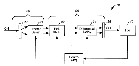
Figure 1 is a chart showing chromatic dispersion wavelength dependence;
Figure 2 is a chart showing chromatic dispersion penalty curves for an ideal
receiver at transmission rates of lOG/s and 40Gb/s;
Figure 3 is a chart illustrating the sensitivity of different receivers to
chromatic
dispersion;
Figure 4 is a chart showing the wavelength dependency of polarization mode
dispersion;
Figure 5 is a chart showing approximate PMD power penalty curves for IOGb/s
and 40Gb/s optical transmission speeds;
Figure 6A is a block diagram of a communications system employing the
integrated dispersion compensation system of the present invention;
Figure 6B is a block diagram of an integrated dispersion compensation system
for performing dispersion compensation.in accordance with one embodiment of
the
present invention;
Figure 7 is a block diagram of an integrated dispersion compensation system
for
performing dispersion compensation in accordance with an alternate embodiment
of the
present invention;
5
CA 02465518 2004-04-30
WO 03/040777 PCT/US02/33855
Figure 8 is a method of performing dispersion compensation in accordance with
another embodiment of the present invention; and
Figure 9 is a method of performing dispersion compensation in accordance with
yet another embodiment of the present invention.
DETAILED DESCRIPTION
Reference will now be made in detail to the present exemplary embodiments of
the invention, examples of which are illustrated in the accompanying drawings.
Wherever possible, the same reference numbers will be used throughout the
drawings
to refer to the same or like parts. An exemplary embodiment of the integrated
dispersion compensation system of the present invention is shown in Figure 6,
and is
designated generally throughout by reference numeral 10.
In accordance with the invention, the present invention is directed to an
integrated system for performing dispersion compensation on at least one
wavelength
channel. The system includes a tunable integrated dispersion compensation
module
configured to perform chromatic dispersion (CD) compensation and polarization
mode
dispersion compensation (PMD) on the at least one wavelength channel. A
feedback
element is coupled to the integrated dispersion compensation module. The
feedback
element is configured to provide at least one feedback control signal to
thereby adjust
the tunable integrated dispersion compensation module until a predetermined
characteristic of the at least one wavelength channel is optimized. Thus, the
present
invention provides an integrated approach to CD and PMD compensation. As
described below, the present invention also helps to compensate for higher
order PMD
as well. The integrated dispersion compensation method of the present
invention can
be employed to optimize any specific receiver's performance. Further, the
integrated
dispersion compensation method of the present invention can be employed to
optimize
any given transmitter-receiver combination.
As embodied herein, and depicted in Figure 6A, a block diagram of a
communications system employing the integrated dispersion compensation system
of
the present invention is disclosed. Individual channel transmitters 2 are
coupled to
multiplexer 4 to create a multiplexed signal (Ch 1-Ch N). The multiplexed
signal is
transmitted by way of optical fiber 6. Subsequently, the multiplexed signal is
amplified
by amplifier 8 and re-transmitted on fiber 6 to demultiplexer 12. In the
current state of
6
CA 02465518 2004-04-30
WO 03/040777 PCT/US02/33855
the art, amplifier 8 typically includes a dispersion compensation module.
However, CD
cannot be perfectly compensated for all channels. Usually there is a residual
CD for
different channels, and the slope compensation is not perfect. Demultiplexer
12
demultiplexes the multiplexed signal into its constituent channels. Each
channel is
provided to integrated dispersion compensation system 10 for tunable
compensation.
Thus, CD compensation and PMD compensation (ls' order and higher order) are
performed for each channel.
It will be apparent to those of ordinary skill in the pertinent art that any
suitable
means may be used to implement multiplexer 12 and demultiplexer 4, but there
is
shown by way of example a diffraction grating. Those of ordinary skill in the
art will
recognize that prism based devices may also be used.
As embodied herein, and depicted in Figure 6B, a block diagram of an
integrated dispersion compensation system 10 for performing dispersion
compensation
in accordance with one embodiment of the present invention is disclosed.
System 10
includes tunable chromatic dispersion (CD) compensation portion 20 coupled to
polarization mode dispersion (PMD) compensation portion 30. CD compensation
portion includes dispersive element 22 coupled to tunable delay unit 24. As
described
above, CD leads to pulse broadening because different frequency components
travel
faster or slower than other frequency components. Thus, dispersive element 22
breaks
channel (i ) into its various frequency components. The faster components are
delayed
by tunable delay 24 causing the various components to be time aligned. Because
chromatic dispersion is also wavelength dependent, each wavelength channel is
adjusted individually for chromatic dispersion.
It is noted that the above described CD compensation also corrects second
order
PMD. PMD is often presented as a series of first order, second, and higher
order PMD.
Second order PMD includes a term which is similar to CD, so called
polarization
dependent CD. This part of the second order PMD is also compensated for by CD
portion 20. PMD is characterized by two orthogonal states of polarization
called the
principal states (PSP) and the differential group delay. PMD is described
mathematically using a Stokes vector:
7
CA 02465518 2004-04-30
WO 03/040777 PCT/US02/33855
SZ = ~i~q (1)~
where ~i is the DGD value and q is a unit vector pointing in the direction of
the fast
PSP. Second order PMD is obtained by differentiation:
~w = ~i~,~q + ~i~q~, (2)~
where "w" denotes differentiation. The derivative of DGD with respect to
frequency is
Di~,. In other words, a~ac~ = Diw, which is a term that is similar to
chromatic
dispersion. Thus, by compensating for CD, this term is also compensated.
PMD compensation portion 30 compensates for first order PMD. PMD
compensation portion 30 includes polarization controller 32 disposed between
tunable
delay unit 24 and differential delay 34. Polarization controller 32 functions
to ensure.
that differential delay 34 receives exclusively the "slow-mode" component and
the
"fast-mode" component for the particular wavelength channel. Delay unit 34
introduces unequal time delays between the components of each wavelength
channel.
Each applied delay must be opposite and equal to the time difference between
the fast
mode pulse and the slow mode pulse, if the fast mode pulse and the slow mode
pulse
are to be time aligned. Note that this compensates for higher PMD because the
PSP for
pulse frequency polarization components is controlled.
Differential delay unit 34 is coupled to beam combiner unit 36. Beam combiner
36 recombines the frequency components of the channel. Beam combiner 36
provides
receiver 40 with a dispersion compensated wavelength channel. Control
electronics 42
is coupled to differential delay unit 34, polarization controller 32, and to
tunable delay
unit 24. Essentially, receiver 40 provides control electronics with a bit-
error rate
(BER), a DGD value, or a Q-factor for the channel. Control electronics 42
derives a
feedback control signal to control each of the elements with system 10. Thus,
integrated dispersion compensation system 10 utilizes feedback control signals
to
optimize BER or the Q-factor, or any other selected performance
characteristic.
Those of ordinary skill in the art will recognize that tunable CD element 24
or
differential delay 34 can be implemented using a free-space device or a fiber
device.
For example, both of these elements can be implemented using a tunable chirped
fiber
8
CA 02465518 2004-04-30
WO 03/040777 PCT/US02/33855
Bragg grating. The delay can be adjusted mechanically or by using a
temperature based
actuator.
As embodied herein and depicted in Figure 7, a block diagram of integrated
dispersion compensation system 10 for performing dispersion compensation in
accordance with an alternate embodiment of the present invention is disclosed.
In this
embodiment, CD compensation and PMD compensation are performed simultaneously.
System 10 includes polarization controller 50 coupled to dispersive element
52. As
discussed above, polarization controller ensures that the substantially the
fast mode and
slow mode polarization components are provided to tunable delay 56.
Subsequently,
dispersion compensated polarization components for the channel are provided to
beam
combiner 58. Receiver 400 measures the bit-error rate (BER), the DGD value, or
the
Q-factor for the channel. Feedback control electronics 402 uses this
information to
derive feedback control signals for both polarization controller 50 and
tunable delay 56
to thereby optimize BER, the Q-factor, or any other receiver performance
criteria.
As embodied herein, and~depicted in Figure 8, a method for performing
dispersion compensation in accordance with another embodiment of the present
invention is disclosed. The method of Figure 8 is stored in memory in the
control
electronics in receiver 40 (first embodiment), or the control electronics 402
in the
second embodiment. These devices will be referred to as the "controller" in
the
following description. In step 802, the receiver, or an optical monitor in the
receiver,
measures the Q-factor, BER, or some other relevant measurement characteristic.
A
histogram or eye-diagram may also be used. Those of ordinary skill in the art
will
recognize that any suitable method may be employed to measure receiver
performance
depending on the sophistication of the receiver electronics and the control
electronics.
In step 804, the control electronics compares the measured characteristic with
a
predetermined optimal range of characteristic values. If the measured
characteristic is
within the optimal range, no compensation is performed, and the controller
stores the
CD value, the DGD value with the measured characteristic (Q-factor, BER,
etc.). If the
measured characteristic is not within the optimal range, the controller
performs CD
compensation in step 808. The controller uses a feedback control signal to
tune CD
9
CA 02465518 2004-04-30
WO 03/040777 PCT/US02/33855
compensation portion 20. After CD is optimized, the receiver/controller uses a
feedback control signal to tune PMD compensation portion 30. Once the measured
characteristic is driven into the optimal range, program flow is directed to
step 812 and
the controller stores the CD value, the DGD value with the measured
characteristic in
step 814.
As embodied herein and depicted in Figure 9, a method for performing
dispersion compensation in accordance with yet another embodiment of the
present
invention is disclosed. The method of Figure 9 is stored in a memory in the
control
electronics in receiver 40 (first embodiment), or the control electronics 402
in the
second embodiment. Again, these devices will be referred to as the
"controller" in the
following description. In step 902, the receiver, or an optical monitor in the
receiver,
measures the Q-factor, BER, or some other relevant measurement characteristic.
In
step 904, the control electronics compares the measured characteristic with a
predetermined optimal range of values. If the measured characteristic is
within the
optimal range, no compensation is performed, and the controller stores the CD
value,
the DGD value with the measured characteristic. If the measured characteristic
is not
in an optimal range of values, the controller performs steps 906 and 908
substantially
simultaneously using one feedback control signal to tune CD compensation
portion 20
and another feedback control signal to tune PMD compensation portion 30. Once
the
measured characteristic is driven into the optimal range, program flow is
directed to
step 910, and the controller stores the CD value, the DGD value with the
measured
characteristic in step 912.
It will be apparent to those skilled in the art that various modifications and
variations can be made to the present invention without departing from the
spirit and
scope of the invention. Thus, it is intended that the present invention cover
the
modifications and variations of this invention provided they come within the
scope of
the appended claims and their equivalents.