Note: Descriptions are shown in the official language in which they were submitted.
CA 02465847 2004-05-05
WO 03/053270 PCT/US02/41097
SYSTEM FOR EXCITATION LEADLESS MINIATURE MARKER
CROSS REFERENCE TO RELATED APPLICATIONS
This application is a continuation-in-part of U.S. Patent Application No.
10/027,675, titled SYSTEM FOR EXCITATION OF-- LEADLESS- MINIATURE
MARKER, filed December 20, 2001.
TECHNICAL FIELD
This invention relates to systems for activating miniature markers, and more
particularly to systems for excitation of resonating miniature marker
assemblies for
use in locating the markers in three-dimensional space.
BACKGROUND OF THE INVENTION
Systems have been developed to activate and defect remote activatable
marker assemblies positioned, as an example, in or on a selected item or
object.
The markers generate a signal used to detect the presence of the marker. Many
of
the activatable markers are hard-wired to a power source or other equipment
external from the object. Other systems have been developed that utilize
resonating
leadless markers, also referred to as wireless active markers, positionable at
or near
a selected target. These wireless active markers are typically activated or
energized by a remote excitation source that generates a strong continuous
excitation signal. Accordingly, the markers generate a detectable marker
signal that
must be distinguished from the strong continuous excitation signal and then
analyzed in an effort to try to accurately determine the target's location.
The
process of distinguishing a weak marker signal from the strong continuous
excitation
signal, while maintaining sufficient accuracy and repeatability for
determining the
marker's location, has proven to be very difficult.
Other systems have provided detection of leadless markers to determine a
two-dimensional proximity (e.g., X, Y coordinates) to detectors for use with
game
boards, surgical tag detection devices, and medical tube placement
verification
CA 02465847 2004-05-05
WO 03/053270 PCT/US02/41097
systems. In the case of the game boards, a unique game piece with a resonator
of a
predetermined frequency is moved across the game board, and the X and Y
location
ordinates of the game piece relative to the game board are displayed so the
players
can determine the general location of the game piece on the game board. U.S.
Patent No. 5,853,327 to Gilboa identifies that the X, Y coordinates, as a
function of
amplitude or phase, may be determined experimentally for a given game board
design. Additionally, Z distance away from the game board may be determined to
a
sufficient accuracy for game use by the strength of the signal above the game
board
provided that the signal is not a strong function of the X and Y locations.
U.S.
Patent No. 5,188,368 to Ryan provides a system for determining in two
dimensions
which individual square of a chess board a particular chess piece is on during
a
chess game. The system disclosed by Ryan does not determine the Z direction.
In the case of the surgical tag and detection device, U.S. Patent No.
6,026,818 to Blair discloses surgical devices, such as sponges, that have
activatable resonator tags thereon. A probe with an interrogation ring is
provided
that can be scanned over an area of a patient after surgery to determine if
any
surgical devices having the resonator tags have been left behind. Therefore,
the
detection device of Blair is only detecting the existence or proximity of a
surgical tag
with the interrogation ring, rather than the actual location of the
activatable tags.
In the case of the medical tube placement verification device, U.S. Patent No.
5,325,873 to Hirschi et al. teaches a system that detects the general position
of an
object within a body of tissue. The detection system includes a resonant
circuit
attached to the object and a separate detection probe having a visual display
indicating the direction which the probe should be moved to center the
detection
probe over the object.
The systems of the above patents activate the markers with a pulsed
excitation signal generated by driving an untuned source coil with either a
unipolar
polarity to produce a wide band impulse function or a bipolar polarity to
create a
waveform that more closely matches the desired resonant frequency of the
marker.
The required levels of magnetic excitation for the markers in the above
patents are
relatively low such that the excitation energy in the source coil is
substantially
consumed after each pulse due to the pulse circuitry resistive losses. The
source
-2-
CA 02465847 2004-05-05
WO 03/053270 PCT/US02/41097
coils are driven by linear amplifiers, and in one case by linear amplifiers at
both
ends of the coil, and by a simple pulse network that energizes the coil and
extinguishes resistively. The amplitude of the pulsed excitation signal
required for
these applications is relatively low since either the resonator circuit to be
located is
of a large size, the volume in which the resonator must be located is
relatively small,
or the accuracy requirements locating the resonator are quite low.
Accordingly, the
existing systems are not suitable for use in many situations wherein highly
accurate
determinations of the marker's location in three-dimensional space is
required. The
existing systems may also not be suitable for use with efficient, high energy
systems
for energizing the marker assemblies so as to provide a sufficient marker
signal for
use in determining the location of the marker in three-dimensional space
relative to
remote sensors.
Other systems have been developed for proximity detection of resonator tags
for Electronic Article Surveillance (EAS) systems. The requirements for EAS
systems are to detect the presence of a security tag within a six-foot wide
aisle
using one antenna assembly for both excitation and detection of the tag within
the
aisle. Some EAS systems utilize tuned resonant excitation source coil drive
circuitry
for pulsed resonator tag operation. As an example, U.S. Patent No. 5,239,696
to
Balch et al. discloses a linear amplifier using current feedback linear power
amplifiers to drive an excitation source tuned to resonant coils for use in
pulsed EAS
systems. The current feedback is used to adjust the linear amplifier's drive
current
level provided to the tuned excitation source coil load. The current feedback
is also
used to provide for a relatively constant current drive for exciting resonant
EAS tags
in the field. The source coil is tuned to allow for use of a simple, low
voltage linear
amplifier circuit design. The source coil current pulse waveform is determined
by
the summation of the sinusoidal control signal and the drive current feedback
signal
input to the linear amplifier.
U.S. Patent No. 5,640,693 to Balch et al. discloses the use of linear power
amplifiers to drive tuned excitation source coils for use in pulsed EAS
systems. An
apparatus for switching power to a linear amplifier is provided to turn to an
"on" state
and an "off' state used to control the output drive pulse burst of the tuned
excitation
source coils. Balch et al. '693 also identifies that linear amplifiers that
generate
-3-
CA 02465847 2004-05-05
WO 03/053270 PCT/US02/41097
drive signals for a tuned source coil since linear amplifiers are typically
only about
thirty to forty percent efficient. The inherent inefficiency of the linear
amplifier drive
is improved by switching the amplifier power "on" and "off' at the same time
that the
pulse control input signal to the power supply is switched "on" and "off'
position.
U.S. Patent No. 5,815,076 to Herring teaches one of more damping circuits
provided in series with excitation source coils and used to promote rapid
dampening
of the pulsed excitation interrogation signals at the end of each signal
pulse.
Providing the switchable damping circuits in series with the antennas
increases the
power dissipation of the device during pulse delivery due to added damping
circuit
switch resistance in the antenna current path.
The above systems employ a resonator circuit energized with a pulsed
excitation signal and the resonator response signal is measured with sensing
coils.
The amplitude of the pulsed excitation signal required for these applications
is
relatively low since either the resonator circuit to be located is of a large
size, the
volume in which the resonator must be located is relatively small, or the
accuracy
requirements locating the resonator are quite low.
SUMMARY OF THE INVENTION
Under one aspect of the invention, a system is provided for generating a
magnetic field for excitation of a leadless marker assembly. The system
includes a
source generator assembly having a power supply, an energy storage device, a
switching network and an untuned source coil interconnected and configured to
deliver a selected magnetic excitation signal waveform, such as continuous
bipolar
or unipolar waveform, or a pulsed waveform. In one embodiment, the waveform
can
be configured to contain sufficient energy at the selected leadless marker
resonant
frequency to energize the marker sufficiently above the ambient environment
background noise. Also, the waveform can be programmable in both pulse
frequency and pulse duration. For example, the frequency may be programmed to
be a single repetition frequency or a composite of two or more repetition
frequencies. The duration can be programmed from a continuous wave (CW)
waveform of repetitive pulses essentially continuous in nature to a single
pulse burst
of a discrete number of pulses that has a defined pulse burst repetition rate.
In a
-4-
CA 02465847 2004-05-05
WO 03/053270 PCT/US02/41097
continuous wave (CW) embodiment, the marker signal is measured while the
source
signal is substantially present. In a pulsed embodiment, the marker signal is
measured after the source signal has been extinguished and is not
substantially
present. The power supply can be configured to deliver power to energize the
energy storage device. The switching network can be configured to direct
electrical
current through the source coil to generate a pulsed magnetic field;
alternately
switch between a first "on" position and a second "on" position; alternately
switch
between the first and second "on"; alternately transfer stored energy from the
energy storage device to the source coil and to transfer stored energy from
the
source coil back to the energy storage device when switching between the first
and
second "on" positions; and the untuned source coil being coupled to the
switching
network to generate a selected excitation signal.
Other embodiments of the invention can have other features. Other
embodiments are directed toward methods.
BRIEF DESCRIPTION OF THE DRAWINGS
Figure 1 is a schematic isometric view of a system for energizing and locating
leadless miniature markers in accordance with an embodiment of the present
invention.
Figure 2 is an isometric view of an embodiment of an implantable miniature
resonating marker assembly usable in the system of Figure 1.
Figure 3 is a schematic block diagram of the excitation system of Figure 1
illustrating a source signal generator, a signal processing device, a sensor
array,
and leadless markers.
Figure 4 is a schematic block diagram of an embodiment of the source signal
generator of Figure 3.
Figure 5 is a schematic voltage diagram showing the voltage across a source
coil of the system of Figure 1 during excitation "on" and excitation "off'
phases over
time for the pulsed excitation and location of the marker assembly.
Figure 6 is a schematic bipolar current diagram during the excitation "on" and
excitation "off' phases over time of Figure 5 for pulsed excitation and
location of a
marker assembly.
-5-
CA 02465847 2004-05-05
WO 03/053270 PCT/US02/41097
Figure 7 is a schematic electrical diagram of an alternate embodiment of the
system of Figure 3, the system including a pulse extinguishing circuit.
Figure 8 is a schematic voltage diagram showing the voltage across a source
coil of the system of Figure 1 during excitation phases over time for the
continuous
wave (CW) excitation and location of the marker assembly.
Figure 9 is a schematic bipolar current diagram during the excitation phase
and over time of Figure 8 for the continuous wave (CW) excitation and location
of
the marker assembly.
DETAILED DESCRIPTION
In the following description, certain specific details are set forth in order
to
provide a thorough understanding of various embodiments of the invention.
However, one skilled in the art will understand that the invention may be
practiced
without these details. In other instances, well-known structures associated
with
magnetic excitation systems, resonating markers, and activators have not been
shown or described in detail to avoid unnecessarily obscuring the description
of the
embodiments of the invention.
Figures 1-9 illustrate a system and components for generating an excitation
signal for activating a resonating marker assembly and locating the marker in
three-
dimensional space in accordance with embodiments of the present invention.
Several of the components described below with reference to Figures 1-9 can
also
be used in systems for performing methods in accordance with aspects of the
present invention. Therefore, like reference numbers refer to like components
and
features throughout the various figures.
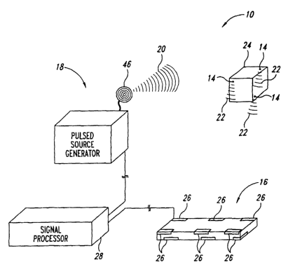
Figure 1 is a schematic isometric view of a system 10 for energizing and
locating one or more leadless resonating marker assemblies 14 in three-
dimensional space relative to a sensor array 16 in accordance with one
embodiment
of the present invention. The system 10 includes a source generator 18 that
generates a selected magnetic excitation field or signal 20 that energizes the
marker
assemblies 14. The energized marker assemblies 14 generate a measurable
marker signal 22 that can be sufficiently measured in the presence of both the
excitation source signal and environmental noise sources. In the illustrated
-6-
CA 02465847 2004-05-05
WO 03/053270 PCT/US02/41097
embodiment, the marker assemblies 14 are positioned in or on a selected object
24
in a known orientation relative to each other. The marker signals 22 are
measured
by a plurality of sensors 26 in the sensor array 16. The sensors 26 are
coupled to a
signal processor 28 that utilizes the measurement of the marker signals 22
from the
sensors 26 to calculate the location of each marker assembly 14 in three-
dimensional space relative to a known frame of reference, such as the sensor
array
16.
In the illustrated embodiment, as discussed in greater detail below, the
source generator 18 is configured to generate the excitation signal 20 so that
one or
more marker assemblies 14 are sufficiently energized to generate the marker
signals 22. In one embodiment the source generator 18 can be switched off
after
the marker assemblies are energized. Once the source generator 18 is switched
off, the excitation signal 20 terminates and is not measurable. Accordingly,
the
sensors 26 in the sensor array 16 will receive only the marker signals 22
without any
interference or magnetic field distortion induced by the excitation signal 20.
Termination of the excitation signal 20 occurs before a measurement phase in
which
marker signals 22 are measured. Such termination of the excitation signal
before
the measurement phase when the energized marker assemblies 14 are generating
the marker signals 22 allows for a sensor array 16 of increased sensitivity
that can
provide data of a high signal to noise ratio to the signal processor 28 for
extremely
accurate determination of the three-dimensional location of the marker
assemblies
14 relative to the sensor array or other frame of reference.
The miniature marker assemblies 14 in the system 10 of the illustrated
embodiment are inert, activatable assemblies that can be excited to generate a
signal at a resonant frequency measurable by the sensor array 16 remote from
the
target 24. In one embodiment, the miniature marker assemblies 14 have, as one
example, a diameter of approximately 2mm and a length of approximately 5mm,
although other marker assemblies can have different dimensions. An example of
the marker detection system is described in detail in co-pending U.S. Patent
Application No. 09/877,498, titled GUIDED RADIATION THERAPY SYSTEM, filed
June 8, 2001, which is incorporated herein in its entirety by reference
thereto.
CA 02465847 2004-05-05
WO 03/053270 PCT/US02/41097
The illustrated marker assembly 14 includes a coil 30 wound around a
ferromagnetic core 32 to form an inductor. The inductor is connected to a
capacitor
34, so as to form a signal element 36. Accordingly, the signal element 36 is
an
inductor (L) capacitor (C) resonant circuit. The signal element 36 in one
embodiment is enclosed and sealed in an encapsulation member 38 made of
plastic, glass, or other inert material. The illustrated marker assembly 14 is
a fully
contained and inert unit that can be used, as an example, in medical
procedures in
which the marker assembly is secured on and/or implanted in a patient's body.
Other marker assemblies 14 are described in detail in co-pending U.S. Patent
Application No. 09/954,700, titled MINIATURE RESONATING BEACON
ASSEMBLY, filed September 14, 2001, which is also incorporated herein in its
entirety by reference thereto. Other leadless marker assemblies 14 that may be
used are described in detail in U.S. Patent Application No. 091078,982, titled
SYSTEM AND METHOD FOR BRACKETING AND REMOVING TISSUE, filed May,
14, 1998; PCT Application No. PCT/US00/31667 titled SYSTEMS AND METHODS
FOR LOCATING AND DEFINING A TARGET LOCATION WITHIN A HUMAN
BODY, filed November 17, 2000; and PCT/US00/31673, titled SYSTEMS AND
METHODS FOR STABILIZING A TARGET LOCATION WITHIN A HUMAN BODY,
filed November 17, 2000, all of which are incorporated herein in their
entireties by
reference thereto.
The marker assembly 14 is energized, and thus activated, by the magnetic
excitation field or signal 20 generated by the source generator 18 such that
the
marker's signal element 36 generates the measurable marker signal 22. The
strength of the measurable marker signal 22 is high relative to environmental
background noise at the marker resonant frequency, thereby allowing the marker
assembly 14 to be precisely located in three-dimensional space relative to the
sensor array 16.
The source generator 18, in one embodiment, is adjustable to generate a
magnetic field 20 having a waveform that contains energy at selected
frequencies
that substantially match the resonant frequency of the specifically tuned
marker
assembly 14. When the marker assembly 14 is excited by the magnetic field 20,
the
signal element 36 generates the response marker signal 22 containing frequency
_g_
CA 02465847 2004-05-05
WO 03/053270 PCT/US02/41097
components centered at the marker's resonant frequency. After the marker
assembly 14 is energized for a selected time period, the source generator 18
is
switched to the "off' position so the pulsed excitation signal 20 is
terminated and
provides no measurable interference with the marker signal 22 as received by
the
sensor array 16.
The marker assembly 14 is constructed to provide an appropriately strong
and distinct signal by optimizing marker characteristics and by accurately
tuning the
marker assembly to a predetermined frequency. Accordingly, multiple uniquely
tuned, energized marker assemblies 14 may be reliably and uniquely measured by
the sensor array 16. The unique marker assemblies 14 at unique resonant
frequencies may be excited and measured simultaneously or during unique time
periods. The signal from the tuned miniature marker assembly 14 is
significantly
above environmental signal noise and sufficiently strong to allow the signal
processor 28 (Figure 1 ) to determine the marker assembly's identity, precise
location, and orientation in three dimensional space relative to the sensor
array 16
or other selected reference frame.
The system 10 of the illustrated embodiment in Figure 1 can be used in many
different applications in which the miniature marker's precise three-
dimensional
location within an accuracy of approximately 1 mm can be uniquely identified
within a
relatively large navigational volume, such as a volume of 12cm x 12cm x 12cm
or
greater. One such application is the use of the system 10 to accurately track
the
position of targets (e.g., tissue) within the human body. In this application,
the
leadless marker assemblies 14 are implanted at or near the target so the
marker
assemblies move with the target as a unit and provide positional references of
the
target relative to a reference frame outside of the body. Such a system could
also
track relative positions of therapeutic devices (i.e., surgical tools, tissue
ablation
devices, radiation delivery devices, or other medical devices) relative to the
same
fixed reference frame by positioning additional leadless marker assemblies 14
on
these devices at known locations or by positioning these devices relative to
the
reference frame. The size of the leadless markers use on therapeutic devices
may
be increased to allow for greater marker signal levels and a corresponding
increase
in navigational volume for these devices.
_g_
CA 02465847 2004-05-05
WO 03/053270 PCT/US02/41097
The system 10 is configured to generate a sufficient source excitation
magnetic field signal, as an example, source excitation coil Magnetic Dipole
Moment
approximately greater than 0.5A*m2, at the appropriate frequency to energize
the
one or more marker assemblies significantly above the environmental background
noise. The system 10 also generates excitation source magnetic field flux
signals at
orthogonal spatial orientations (e.g., along the X, Y and Z axes) to excite a
marker
assembly 14 that may be a resonator having a single coil substantially
oriented
along a single axis and spatially orthogonal to excitation energy along the
other two
axes. The system 10 can also be configured to generate excitation source
magnetic
field flux signals at variable frequencies to energize a plurality or marker
assemblies
14 that contain resonant circuits tuned to these unique frequencies.
Accordingly;
the multiple marker assemblies 14 can be sequentially or simultaneously
energized.
The system 10 is also configured to avoid the difficult process of separating
the small marker signal 22 from the much more powerful source excitation
signal 20
by measuring the marker signal during a time period when the source signal is
substantially not present. The residual source excitation signal 20 can cause
substantially less accurate results in the location determination if not
controlled.
The system 10 provides for the measurement of the marker signal 22 with a
sufficient number of spatially distributed sensors 26 at a sufficient signal-
to-noise
ratio so that an inversion algorithm provided in the signal processor 28 can
accurately solve for the three-dimensional location of the particular marker
assembly
14 relative to the known reference frame of the sensor array 16.
Figure 3 is a schematic block diagram of the system 10 in accordance with
one embodiment. As seen in Figure 3, the plurality of leadless miniature
marker
assemblies 14 on the target 24 are remote from the source generator 18 and
from
the sensor array 16. The sensor array 16 is operatively coupled to the signal
processing device 28.
The source generator 18 includes a high voltage power supply 40 coupled to
an energy storage device 42. In one embodiment, the power supply 40 is a 500
volt
power supply, although other power supplies with higher or lower voltages can
be
used. The energy storage device 42 in one embodiment is a high voltage
capacitor
that can be charged and maintained at a relatively constant charge by the
power
-10-
CA 02465847 2004-05-05
WO 03/053270 PCT/US02/41097
supply 40. Energy stored in the storage device 42 allows for providing energy
to
and removing energy from the source coil inductor. A small amount of stored
energy is present in the source coil inductor at maximum current relative to
the
energy stored in the energy storage device 42.
The energy storage device 42 is capable of storing adequate energy to
minimize voltage droop in the energy storage device while having a low series
resistance so as to minimize power losses. The energy storage device 42 also
has
a low series inductance to allow for maximum source generator excitation
capability
to drive the source coil 46. Specialized aluminum electrolytic capacitors used
in
flash energy applications may be used in one of the embodiments of system 10.
Alternative energy storage devices can also include NiGd and lead acid
batteries, as
well as alternative capacitor types, such as tantalum, film, or the like.
The source generator 18 of the illustrated embodiment also includes a
switching network 44 coupled between the energy storage device 42 and a
plurality
of untuned source coils 46. The switching network 44 is configured to control
the
polarity of the voltage across the source coils 46 and the resultant current
magnitude and polarity with time through the source coils so that the source
coils 46
each generate the high ~ energy excitation field 20 for activating the maker
assemblies (Figure 1 ).
In the illustrated embodiment, the excitation source coils 46 includes three
coils orthogonally oriented to correspond to the X, Y, and Z axes of a
selected frame
of reference. The three coils will be referred to herein as the X coil 48, Y
coil 50,
and Z coil 52, each of which is configured to provide a magnetic field flux
signal
along the respective X, Y, and Z axes. The X, Y, and Z coils 48, 50, and 52
with
their orthogonal orientation effectively avoid blind spots for excitation of
marker
assemblies 14 and can allow the marker assemblies to be in any orientation
relative
to the source generator 18 and still be highly energized upon activation of
the
excitation source coils 46.
The source coil 46 in the illustrated embodiment is configured to deliver
adequate source excitation magnetic fields, which is defined by the area,
number of
turns, current, and other characteristics of the coil. The source coil 46 is
constructed with conductors designed to minimize power loss due to resistive
losses
-11-
CA 02465847 2004-05-05
WO 03/053270 PCT/US02/41097
as well as resistive losses due to skin effects. Examples include small
diameter wire
wound in a LITZ wire configuration to minimize skin effects, or alternatively,
a thin
sheet of conductor to minimize skin effects. Parasitic interwinding
capacitance of
the source coil inductor and interconnection conductors should also be
minimized to
reduce unintended coil current spikes due to very short switching network
voltage
transition times and other unintended source coil resonant circuit affects.
The switching network 44 in the illustrated embodiment includes a plurality of
switches that control energy flow to the X, Y, and Z coils 48, 50 and 52.
These
switches include X-switches 54 coupled to the X-coil 48, Y-switches 56 coupled
to
the Y-coil 50, and Z-switches 58 coupled to the Z-coil 52. The X-switches 54
include a plurality of activatable switch mechanisms that control the polarity
of the
voltage across the X coil 48 so as to control the polarity of the derivative
with time of
the current flow through the X coil. The Y switches 56 control the polarity of
the
voltage across the Y coil 50 so as to control the polarity of the derivative
with time of
the current flow through the Y coil. Similarly, the Z- switches 58 are
configured to
control the polarity of the voltage across the Z coil 52 so as to control the
derivative
with time of the current flow through the Z coil. The derivative with time of
the
current flow at a particular voltage polarity across a particular source coil
results in
either an increasing or decreasing current ramp with time through the source
coil.
In the illustrated embodiment, each of the X, Y, and Z switches 54, 56, and 58
have an H-bridge configuration with four switch mechanisms controlled to
selectively
direct electrical current through the respective X, Y, or Z coil 48, 50, and
52, thereby
generating a pulsed magnetic field from the respective source coil.
The X, Y, and Z switches 54, 56, and 58 are also each configured to
alternately switch between first and second "on" positions to generate a
current flow
with a bipolar waveform. In the first "on" position, the current flow in one
has a
continually increasing current ramp with time through the respective X, Y, or
Z coil
48, 50 or 52 to generate the magnetic excitation field. In the second "on"
position,
the current flow has a continually decreasing current ramp with time through
the
respective X, Y, or Z coil 48, 50 or 52 to generate the magnetic excitation
field.
Such alternate switching over the pulse waveform period effectively provides
for
alternating the polarity of the current flow from a positive polarity to a
negative
-12-
CA 02465847 2004-05-05
WO 03/053270 PCT/US02/41097
polarity. The X, Y, and Z switches 54, 56, and 58 are also configured to
alternately
transfer stored energy from the energy storage device 42 to the respective X,
Y, or Z
axis source coil 48, 50, or 52 and to transfer the stored energy from the
respective
source coil back to the energy storage device when alternating switching
between
the first and second "on" positions.
The X, Y, and Z switches 54, 56, and 58 in one embodiment are also
configured to move to an "off' position to prevent energy transfer from the
energy
storage device 42 to the respective X, Y, or Z coils 48, 50, or 52. Once the
X, Y, or
Z switch 54, 56, or 58 is switched to the "off' position at the appropriate
time when
the energy (i.e. the current) in the source coil is substantially zero, the
respective X,
Y, or Z coil 48, 50, or 52 no longer generates a magnetic field such that the
pulsed
excitation signal 20 ceases, so only the marker signal 22 emanates from the
marker
assembly 14 is measurable.
In an alternate embodiment, the source generator 18 is configured to provide
a continuous wave excitation signal as the X, Y, and Z switches 54, 56, and 58
alternatively switch between the first and second "on" positions to energize
the
leadless marker assemblies 14. Figure 8 illustrates a schematic voltage
diagram
showing a bipolar voltage across a source coil 64 to generate the continuous
excitation signal, and Figure 9 is a schematic bipolar current diagram of the
continuous excitation signal corresponding to the voltage diagram of Figure 8.
The
X, Y, and Z coils 48, 50, and 52 are untuned coils so that the frequency of
the
excitation signal 20 can be changed or modified to match the different
resonant
frequencies of a plurality of marker assemblies 14. The frequency of the
excitation
signal 20 can be changed after the marker assembly 14 is energized.
Accordingly,
the sensor array 16 and the signal processor 28 can distinguish the marker
signal
22 from the excitation signal by measuring the marker resonant signal while
the
source signal is substantially present but of a different frequency from the
measured
marker frequency. Accordingly, the source signal generator excitation waveform
is
substantially present during measurement of the leadless marker signal 22. The
use of highly energy efficient source generator 18 that drives an untuned
source coil
allows for dynamic adjustment of source coil's continuous waveform excitation
signal
frequency without adjusting or modifying the tuning capacitor of a tuned
resonant
-13-
CA 02465847 2004-05-05
WO 03/053270 PCT/US02/41097
source coil circuit. This feature allows for adjustment of the source coil's
continuous
waveform excitation signal frequency to excite multiple uniquely tuned marker
resonators during different time periods from the same source coil without
modifying
a source coil tuning capacitance that is present in a tuned source coil
embodiment.
Furthermore, an untuned source coil embodiment is not susceptible to source
detuning effects of tuned source coil embodiments.
In another alternate embodiment, the source generator 18 sweeps the
continuous waveform excitation frequency by driving the coil with an
exponential FM
chirp relative to the resonant frequencies of the marker assemblies within the
excitation field 14. One or more marker signals 22 may be then extracted from
the
combined measurement with the excitation signal present because of the
amplitude
and phase characteristics of the marker resonators as a function of frequency.
The
measurement of the combined marker and source signals occurs after the marker
is
energized to steady state condition. The marker signal is then separated from
combined source and marker signal with signal processing.
In another embodiment, the source frequency may be adjusted such that the
marker signal 22 is a lagging 90 degrees phase difference with the excitation
signal
20 when the marker assembly 14 is excited at the resonant frequency of the
marker
assembly. Accordingly, the signal can be distinguished from the marker signal
because the phase difference between the source and one or more marker
signals.
Therefore, different embodiments of the invention may distinguish the marker
signal from the source signal because of time, phase or frequency differences
between the source and one or more marker signals.
The alternating current flow through the X, Y, or Z coil 48, 50, or 52
generates the pulsed magnetic field in the selected axis to excite the marker
assembly 14 located at a determinable distance from the coil. The following is
an
equation for calculation of the magnetic field excitation at a distance from a
source
coil inductor of a solenoid shape:
2
Bmarker (distance) _ ~° ~ Isource ~ rsource ~ Nsourc3
2 ~ (r 2 +Distance2 )z
source
-14-
CA 02465847 2004-05-05
WO 03/053270 PCT/US02/41097
Where:
Bmarker(dlstance) = magnetic field flux density at a distance from the source
coil along the coil axis
o - permeability of free space between the source coil and the marker
assembly
rsou~~e = Radius of the source coil (meters)
Nsouroe = Number of turns of wire around the source coil
Distance = distance from the source coil (meters)
Iso~~~e = Electrical current through source coil (amperes)
The electrical current (Iso,~~e~ through the X, Y, or Z coil 48, 50, or 52 is
determined by the voltage applied across the coil inductance (L). The
inductance
(L) of an air core coil (solenoid) is approximated by:
2 2
L - (14'0 ~ ~ ~ rsource ~ Nsource )
lengthso,~~e
Where:
L = Inductance of the source coil
~,o = permeability of free space
rsou~~e = Radius of the source coil (meters)
Nsouroe = Number of turns of wire around the source coil
lengthso~~~e = Length of source coil (meters)
The inductance of the source coil determines the electrical current derivative
with time through source coil inductor as follows:
V=L*dl/dt or V/L=dl/dt
-15-
CA 02465847 2004-05-05
WO 03/053270 PCT/US02/41097
Where:
V = voltage potential across the coil (volts)
L = Inductance of the source coil
dl I dt = The change in coil current with time
To efficiently transfer energy to a coil and create the magnetic excitation
field,
power losses due to resistance in the source coil circuit should be minimized.
The
power (i.e., RMS power) in the system is determined as follows:
P = I2 RTOTAL
Where:
I = Root Mean Square value of the current
RTOTAL = Total resistance in the source coil circuit
The power losses of the system 10 limits the strength of the magnetic
excitation field that the system is capable of delivering. The strength of the
magnetic excitation field decreases with the cube the distance from the
magnetic
field source (e.g., the source coil 46). Furthermore, the magnetic excitation
field
increases linearly with current, but the power dissipation in the system
increases as
the square of the current. Accordingly, the requirements for source drive
electronics
become more challenging to allow for adequate levels of the marker signal 22
as the
magnetic excitation field requirements increase.
In one embodiment, the source coil 46 can be operated as a tuned circuit
wherein the source coil inductor is tuned with a capacitor chosen for the
desired
resonant frequency of the marker assembly 14. The reactance of the inductor is
equal to and opposite the capacitor at the frequency of interest, such that
only the
resistance of the source coil circuit is seen by the drive electronics.
Substantial
-16-
CA 02465847 2004-05-05
WO 03/053270 PCT/US02/41097
stored energy can occur in the tuned circuit, however, that may limit the time
in
which the source coil excitation signal is shutoff. Longer shut-off time
reduces the
time during which the marker resonator signal can be measured effectively in
the
absence of the source signal. Accordingly, a shorter shutoff time can be very
desirable. A shorter shutoff time also allows for adequate marker ring down
signal
to remain after the source signal has decayed such that the marker signal may
be
measured at a sufficient signal to noise ratio for accurate location of the
marker.
The system 10 of the one embodiment provides an untuned source coil 46
configured to excite the leadless marker assembly's resonator with the pulsed
excitation signal 20 having a high level of source excitation energy. The
system 10
also provides a very short source excitation turnoff time to achieve optimal
performance for measuring the marker signal 22 after the source excitation
signal 20
is significantly extinguished. Accordingly, the turnoff time for an untuned
source coil
can have a significant impact on the effectiveness of the system 10, so the
system is
configured to have only limited stored energy after turnoff time. Therefore,
the
source generator 18 of the system 10 is configured to deliver high source coil
current amplitudes at the optimal marker excitation frequencies to energize
the
leadless markers 14 before the time decaying marker ring down signal is
measured.
Figure 4 is a schematic block diagram of a source generator 18 of one
embodiment. In this illustrated embodiment, a high-voltage power supply 40 and
energy storage device 42 are shown coupled to a single switch network 44,
which
has a single H-bridge switching configuration. This switch network 44 has four
switches 62a-d coupled together so as to control the current flow to a single
source
coil 64. In this embodiment, when multiple source coils are used, each source
coil
is coupled to a separate switch network, power supply, and energy storage
device.
In one embodiment, a common energy storage device and a common power supply
for multiple switching networks and corresponding source coils are used.
The switch network 44 of the illustrated embodiment with the H-bridge
configuration constructed of MOSFET devices. The switching devices have a low
"on" series of resistance (less than or equal to approximately 1 ohm) to
minimize
power losses. Furthermore, very short switching times (less than approximately
25
nanoseconds) are provided to minimize switching induced power losses and
-17-
CA 02465847 2004-05-05
WO 03/053270 PCT/US02/41097
maximum excitation delivery. The short switching times allow for high
frequency
system operation (for example, 50-600 kHz) that improves overall system
performance due to increases in inductive coupling efficiencies between the
source,
marker, and sensor coils with frequency. Alternate embodiments have switch
networks 44 that include one-half H-bridge configurations (having only two
switches)
with a matched set of power supplies and two matched energy storage devices
__._ __ .__ _ __. _.. ___ _ . .__ _ _._. . _ . __._ __ __. ._ __ . _ _._ _ _ _
___ _._ __ .___ .__ ___ _._ ..__ _ ._ _ _ .___ - ternative _
configured to deliver a bipolar voltage drive to the source coil 46. The al
switching components can include bipolar junction transistors (BJT), JFETs,
and
various possible vacuum tube configurations.
The power supply 40 directs charge to and maintains a relatively constant
energy storage level at the energy storage device 42 by delivering average
power to
the energy storage device. The amplitude of the charging current is large
enough to
compensate for average power consumption in the pulse generator and keep the
energy storage device at a relatively constant voltage. The energy storage
capacitor must be large enough to minimize voltage droop during pulse
generation
and capable of both supplying high instantaneous power to the switch network
and
returning high instantaneous power from the switch network 44. The following
example for one embodiment has equations for both calculation of the power
supply
average power and pulse generator instantaneous power delivery:
Veap= SOOV Capacitor charge voltage
Rswitching = 2.0 ohm Total resistance in "on" state (2
switches closed at a time)
Reoil = 0.25 ohm Source coil resistance
~nergy_storage device = 0.05 ohm Energy storage device resistance
IL(rms) = 4.8 amps Source coil rms current
Duty cycle = 50% % of time generator is pulsing
Average power dissipation = (IZsN,itching +' Rcoil + Renergy storage device )
* IL(~S)a *
Duty cycle
PPower_supply (average) _ (2 + 0.25 + 0.05) * (4.8) ' * 0.5 VNatts
PPower_supply (average) = 26 watts
I'instantaneous (dig pulsing) = SOOV * 4.8 amps RMS = 2,400VA RMS
-18-
CA 02465847 2004-05-05
WO 03/053270 PCT/US02/41097
To maintain constant energy storage:
IPower supply (average) = Ppower supply (average) ~ Veap
IPower supply (average) = 26W / 500V = 52milli Ampere
The switch network 44 is configured so pairs of the switches 62a-d are
opened and closed simultaneously when the other pair of switches are
simultaneously closed and opened. As a result, the switch network 44 is
configured
to control the voltage across the source coil 64 in alternating polarities. As
a result,
the current flow through the source coil 64 alternates between positive and
negative
polarity over the pulsed magnetic excitation signal waveform pulse burst time
period.
This alternating of the current flow through the source coil between positive
and
negative polarity results in the pulsed magnetic excitation signal 20 from the
source
coil.
In one embodiment, the switch network 44 moves between the first "on"
position when switches 62b and 62c are closed and switches 62a and 62d are
open,
and the second "on" position when switches 62b and 62c are open and switches
62a and 62d are closed. In this first "on" position, the voltage having a
positive
direction across the source coil 64 increases the current over the pulse "on"
time
through the source coil in the direction of arrow 65. In the second "on"
position, the
voltage having a negative direction across the source coil 64 decreases the
current
over the pulse "on" time through the source coil in the opposite direction of
arrow
65. The resulting pulsed excitation signal due to multiple pulses over the
pulse
burst time period and the repetition frequency of the pulse burst has
determinable
frequency components corresponding to the resonant frequencies of the marker
assemblies 14 for activation of the markers (not shown).
The switch network 44 in the one embodiment also includes an "off" position
that opens the circuit to prevent the current from flowing to the source coil.
Accordingly, no magnetic field is generated and no pulsed excitation signal 20
is
emanated from the source coil 64. The switch network 44 can be switched to the
"off' position by opening switched 62a and 62b and by turning 62c and 62d to a
closed position to shunt the source coil which allows for exponential decay of
-19-
CA 02465847 2004-05-05
WO 03/053270 PCT/US02/41097
residual energy in the source coil. The current then circulates through one of
the
two switches 62c and 62d and one of two H-bridge protection diodes 67 coupled
to
the switches depending on the polarity of the residual current. The residual
current
in the source coil decays by the following exponential time constant:
2 = ~-sc~ ~RL '+' Rswitch '~ Rprotection_diode~
__ ..where; _._
LS~ = Source coil inductance
RL= Source coil resistance
RSWIt~h = Switch "on" resistance
Rprotection_diode = Protection diode "on" resistance
As a result, the switch network 44 is controllable to control the excitation
signal 20 and can be switched to the "off" position to terminate the
excitation signal
after the marker assemblies have been sufficiently energized. When the
excitation
signal is off, the marker signals 22 do not have to be distinguished from the
excitation signal 20 when the marker signal is being measured and analyzed as
discussed above.
In an alternate embodiment, the switch network 44 can be switched to the
"off" position by opening by opening all switches 62a-d. However, care must be
taken to assure that little residual energy remains in the source coil 64 at
the time all
switches are turned "off', otherwise inductive kick back induced voltage
spikes due
to an instantaneous current change through the inductor with time may damage
the
switch network or result in undesired oscillations of the residual current in
the
source coil.
Figure 5 is a schematic voltage diagram showing the bipolar voltage across a
source coil 64 to generate the pulsed excitation signal. The voltage is
controlled by
activating the switch network 44, as discussed above with respect to Figure 4.
When the switch network 44 is switched to the first "on" position, the voltage
across
the source coil 64 is positive as shown in Figure 5 at reference number 66,
thereby
providing a positive polarity. When the switch network 44 is switched to the
second
"on" position, the voltage across the source coil 64 shifts and is negative as
shown
in Figure 5 at reference number 68, thereby providing a negative polarity.
-20-
CA 02465847 2004-05-05
WO 03/053270 PCT/US02/41097
The switch network 44 (Figure 4) alternates between the first and second
"on" positions so as to alternate the voltage across the source coil 64
between the
positive and negative polarities. When the switch network 44 is switched to
the first
"on" position, energy is drawn from the capacitor 42 toward the source coil
64.
When the switch network 44 is switched to the second "on" position, energy is
directed back to the capacitor 42 until the time when the current changes
polarity
and then energy is again drawn from the capacitor. When the switch network 44
is
switched back to the first "on" position, then energy is again directed back
to the
capacitor 42 until the time when the current changes polarity again and then
energy
is again drawn from the capacitor. As a result, the switching network 44 is
configured to alternately transfer stored energy from the energy storage
device 42 to
the source coil 64 and to transfer the storage energy from the source coil
back to
the energy storage device when alternately switching between the first and
second
"on" positions.
In one embodiment, the switch network 44 is configured so that the switches
62a-d (Figure 4) are in the first "on" position for the same total time period
for a
particular pulse burst that they are in the second "on" position. Accordingly,
the
time period at the positive polarity is the same time period as the negative
polarity
for the voltage across the source coil 64. In the embodiment, when the switch
network 44 is switched to the "off' position, the voltage across the source
coil 64 is
zero, as reflected at reference 70 in~the voltage diagram. When the current
through
the source coil 64 (Figure 4) is zero, the source coil provides no excitation
signal 20
that would interfere with the marker signal 22 generated by the marker
assembly 14
as discussed above.
Figure 6 is a schematic bipolar current diagram corresponding to the voltage
diagram of Figure 5. Referring to Figures 4, 5 and 6, when the switch network
44
(Figure 4) is in the first "on" position corresponding so the voltage has a
positive
polarity 66 (Figure 5), the current flow through the source coil 64 (Figure 4)
has a
continually increasing current ramp 70 (Figure 6) so as to generate the
magnetic
excitation field 20 with the positive polarity. When the switch network 44
(Figure 4)
is in the second "on" position corresponding to the negative polarity 68
(Figure 5),
the current flow has a continually decreasing current ramp 72 (Figure 6). When
the
-21-
CA 02465847 2004-05-05
WO 03/053270 PCT/US02/41097
switch network 44 switches back to the first "on" position, the current flow
switches
back to an increasing current ramp 70. Accordingly, the current flow has a
bipolar,
generally non-sinusoidal triangular shaped waveform.
As seen in Figure 6, when the current flow switches directions, for example
from the decreasing current ramp 72 to the increasing current ramp 70, there
is a
point shown at 74 at which the current in the source coil is substantially at
zero
amps. Similarly, when the current flow has the decreasing current ramp 72,
there is
a point shown at 76 at which the current in the source coil 64 (Figure 4) is
at zero
amps. The switch network 44 is configured to switch to the "off" position when
the
current flow through the source coil 64 is substantially at these zero points
74 and
76, and thus at zero amps. When the current in the source coil 64 approaches
zero
amps, the signal decay time for the pulsed excitation signal 20 approaches
zero,
such that the pulsed excitation signal is substantially instantaneously shut
off so as
to provide no interference with the marker signal 22 generated by the
energized
marker assembly 14.
In the embodiment wherein the excitation signal 20 is a CW signal, the switch
network 44 continually switches between the first and second "on" positions
during
the time period when the marker signal is measured. In the pulsed excitation
signal
embodiment wherein the excitation signal is terminated when the switch network
44
is switched to the "off" position, the extent of signal decay over time of the
source
coil 64 current is a function of the resistance in the switch network as well
as
resistance and inductance in the source coil circuitry. In the illustrated
embodiment,
the switch network 44 and source coil 64 are configured such that when the
switch
network is switched to the "off' position, any pulsed excitation signal 20
from the
source coil is immeasurable within approximately one cycle of the energized
marker
assembly. Therefore, the sensor array 16 (Figure 1 ) and the signal processor
28
are configured to begin measuring the marker signal 22 after one cycle of the
marker assemblies 14.
Figure 7 is a block diagram of a source signal generator 90 having a pulse
extinguisher circuit 100 therein in accordance with an alternate embodiment.
In this
alternate embodiment, the source signal generator 90 includes the power supply
40
and the energy storage device 42 coupled to the switch network 44 similar to
the
-22-
CA 02465847 2004-05-05
WO 03/053270 PCT/US02/41097
embodiments discussed above. The switch network 44 is also coupled to the
source coil 64. The switch network 44 is also connected to the pulse
extinguisher
circuit 100 in parallel with the source coil inductor, such that the pulse
extinguisher
circuit does not conduct current during pulse generation. The source signal
generator 90 of this alternate embodiment provides the switch network 44
moveable
between the first "on" position, the second "on" position as discussed above,
and an
"off" position where all of the switches, 62a - 62d, are opened. When the
switch
network 44 is switched to the "off' position, the pulse extinguisher circuit
100
switches 104 are closed to quickly dissipate the residual energy in the source
coil
64 so as to limit the time that an excitation field continues to be generated
after the
switch network has been moved to the "off" position.
The pulse extinguisher circuit 100 is configured to include a pair of
resistors
102 and switches 104 that can be activated to quickly dissipate the residual
energy
in the source coil when the circuit is closed and to interrupt the current
flow through
the extinguisher circuit when the switches 104 are open during excitation
pulse
generation. At the end of a pulse burst, the residual source coil current is
conducted through one of the two switches 104, one of the two resistors 102
and an
H-bridge protection diode 105, depending on the polarity of the residual
current.
Pairs of switches 104 and resistors 102 are provided so the residual current
may be
either of a positive or negative polarity. The time constant for de-energizing
the
source coil inductor is determined by the following equation:
~ = Lsc ~ ~RL + Rswitch + Rprotection diode + Rpulse extinguisher
Where:
LS~ = Source coil inductance
RL= Source coil resistance
Rsw;t~h = Switch "on" resistance
Rprotection diode = Protection diode "On" resistance
Rpulse extinguisher= Pulse extinguisher resistor resistance
The pulse extinguisher circuit's resistors 102 decrease the exponential decay
time constant of residual current in the source coil by adding additional
resistance to
-23-
CA 02465847 2004-05-05
WO 03/053270 PCT/US02/41097
the source coil circuit only during turnoff time. As a result, the pulse
extinguisher
circuit 100 decreases the turnoff time of the source generator and does not
decrease the overall energy efficiency or power dissipation of the source
signal
generator 90.
In the illustrated embodiment, the pulse extinguisher circuit 100 is
configured
so that no measurable or detectable excitation field remains after the switch
network
44 has been moved to the "off' position within less than one cycle of the
resonating
marker assembly 14 (Figure 1 ). Accordingly, the pulse extinguisher circuit
100
facilitates the termination of the pulsed excitation signal 20 so that the
resonating
marker assembly 14 can be easily detectable and located with the signal
processing
assembly 28 to accurately identify the three-dimensional location of the
resonating
marker assembly relative to the sensor array 16.
While the pulse extinguisher circuit 100 is defined in the illustrated
embodiment as providing the resistors 102 and switches 104, with additional
protection diodes 105, other pulse extinguisher circuits can be used so as to
increase the resistance of the total source coil circuit when the switch
network is in
the "off" position. The alternate pulse extinguisher circuits should not
increase
system power dissipation and decrease energy efficiency by adding additional
switch resistance during pulse delivery because of its presence.
Although specific embodiments of, and examples for, the present invention
are described herein for illustrative purposes, various equivalent
modifications can
be made without departing from the spirit and scope of the invention, as will
be
recognized by those skilled in the relevant art. The teachings provided herein
of the
present invention can be applied to systems for excitation of leadless
miniature
markers, not necessarily the exemplary system generally described above.
From the foregoing it will be appreciated that, although specific embodiments
of the invention have been described herein for purposes of illustration,
various
modifications may be made without deviating from the spirit and scope of the
invention. Accordingly, the invention is not limited except as by the appended
claims.
-24-