Note: Descriptions are shown in the official language in which they were submitted.
CA 02466766 2004-05-10
HOUSING FOR RECEIVING A LIGHT SENSOR AND DEVICE
FOR DETECTING OF UV RADIATION
The invention relates to the field of ultraviolet (UV) radiation.
The invention particularly relates to UV devices such as are used in the
pharmaceutical industry. Such UV devices serve for disinfection of waste
water. The
sensors of the devices indicate the UV intensity (W/mz; mW/cmz). Further, such
sensors
monitor such UV devices for unacceptably low intensity, and trigger alarm, if
necessary.
The conventional devices for detecting of UV rays comprise the said sensor as
an essential component which is enclosed by a housing.
1o The whole device, particularly the sensor housing, has to meet various
rigorous requirements. First, such a device has to perform its function -
i.e., it has be able
to detect the UV radiation reliably and precisely. Further, the device
including each of its
components should be of relatively simple design in order to minimize the cost
of
manufacture. Still further, the device should be relatively easy to assemble.
Still further,
the device should be relatively maintenance free. Still further, in the
pharmaceutical
industry cleanness of the parts involved is of great importance.
Conventional devices are disadvantageous since they only partly achieve these
requirements.
It is the object of the present invention to provide a novel device which
obviates or mitigates the above-mentioned disadvantage of the prior art.
It is another object of the present invention to provide a device for
detecting of
UV radiation, and particularly the sensor housing thereof, which device,
compared to the
prior art: is of simple design, is easy to assemble, has low maintenance
requirements, and
may be kept clean over a long period of time, respectively, and has a low
tendency of the
development of germs.
Accordingly, in one of its aspects, the present invention provides a housing
for
receiving of an UV sensor comprising:
1
CA 02466766 2004-05-10
a wall which encloses the sensor;
the wall comprises a region of incidence facing one or several UV
radiation sources (1) as well as a region opposite to the UV radiation sources
(1);
at least the region of incidence consists of a material transparent to UV
rays;
the whole sensor housing (4) respectively the sensor housing (4) without
the region opposite to the UV radiation source (1) is made of one single piece
and free of
openings.
In another of its aspects, the present invention provides a device for the
1o detection of an UV radiation comprising:
at least one UV radiation source ( 1 );
a radiation chamber (3) enclosing the radiation source (1);
a sensor device with a sensor housing (4) the wall of which encloses a
sensor;
the wall of the sensor housing (4) comprises a region of UV radiation
incidence facing the UV radiation source (1) as well as a region opposite to
the UV
radiation source (1);
at least the region of incidence consists of a material which is transparent
to UV radiation;
2o the whole sensor housing (4) respectively the sensor housing (4) without
the region opposite to the UV radiation source (1) is made of one single piece
and is free
of openings.
The main idea of the invention consists in providing a sensor housing
which is enclosed to a large extent, without perforations or openings, without
quartz
windows, O-rings, threaded treasurings, press fit stuffings or sealing means.
Preferably,
the wall is made of one single piece (i.e., it is of unitary construction).
Preferably, it is
made by casting or by die forging or by machining such as turning on a lathe.
In
particular, the wall is closed on that side which faces the UV radiation
source.
2
CA 02466766 2004-05-10
Further, it is important to provide an W transparent material for the sensor
housing, such as Teflon or similar materials or glass. At least that region of
the wall
should consist of such a material which a faces the UV radiation source
(region of
incidence).
There is no need for disassembling an undivided and totally closed sensor
housing of the said type for sanitizing of the UV device by means of steam or
hot water,
which reduces the costs of maintenance as well as the risk of re-germination.
Further, due
to the absence of quartz windows or the like there is no deterioration by
extreme
temperature variations and/or by leakages.
1o Embodiments of the present invention will be described with reference to
the
accompanying drawings, wherein like reference numerals denote like parts, and
in which:
Figures 1-3 each illustrate a sectional view of various embodiments of the
present invention.
Embodiments of the invention are explained more in detail with reference to
the drawings, showing diagrammatically embodiments of the invention.
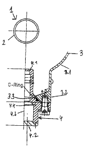
With reference to Figure 1, there is illustrated a radiation source 1 enclosed
by
an enveloping tube 2.
The enveloping tube is housed in a radiation chamber 3. Radiation chamber 3
comprises a chamber wall 3.1. The chamber wall in its lower portion comprises
a
connecting flange 3.2 which is provided with a conical face 3.3, forming a
seat.
A sensor housing 4 is connected to the chamber wall 3.1 of the radiation
chamber 3. Sensor housing 4 surrounds a sensor (not shown). The sensor
receives the
radiation from a radiation source 1.
The sensor housing 4 comprises a main portion 4.1 and a cover 4.2. Main
portion 4.1 consists of a material that is non-transparent with respect to UV-
radiation. An
example of such a material is TeflonTM. Sensor housing 4 essentially is of
cylindrical
shape. In the embodiment shown, it consists of an upper, relatively long
cylinder and a
3
CA 02466766 2004-05-10
lower, relatively short cylinder. The axes 4.3 of both cylinders in general
pass through
radiation source 1.
A UV device may comprise one or several UV radiation sources, located in
the center according to specific patterns and arranged concentrically.
Main portion 4.1 of sensor housing 4 consists of one single piece (i.e.,
unitary
construction). The wall is completely closed, also at the end face (region of
incidence),
facing radiation source 1.
Cover 4.2 in the present case is made of TeflonTM. It may, however, be made
of any other material which is transparent UV radiation. Cover 4.2
mechanically is
o fixedly connected to main portion 4.1 - e.g., by screws, or by press fitting
or by shrink
fitting. Cover 4.2 permits the assembly of the sensor as well as of an
amplifier. The
sensor cable may be past through cover 4.1 by means of a thread nipple.
Instead, it may
be lead out of the housing at a site thereof.
Main portion 4.1 is provided with a circumferential flange 4.4.
Circumferential flange 4.4 comprises a seat 4.5 complementary to seat 2.3 of
connecting
flange 3.2 of chamber wall 3.1. Assembling is very easy by means of the said
seats 3.3,
4.5. Sensor housing 4 when being inserted into the opening of chamber wall 3.1
will get
centered automatically.
As may be seen, both parts, chamber wall 3.1 and main portion 4.1 of sensor
2o housing 4, are fixedly connected to each other by screws. Also, there is
provided a seal
ring at face 4.5. Such seal ring also may be inserted in connecting flange 3.2
of chamber
wall 3.1.
Accordingly, the interior of sensor housing 4 is hermetically sealed with
respect to the environment. Normally, the interior of sensor housing 4 in
addition to the
2s sensor houses an amplifier.
Also with the embodiment according to Figure 2 there is a radiation source 1.
Radiation source 1 is enclosed by an enveloping tube 1.1 made of quartz.
Radiation
4
CA 02466766 2004-05-10
source 1 and enveloping tube 1.1 are located inside of a radiation chamber 3
comprising a
chamber wall 3.1. A sensor housing 4 is connected to chamber wall 3.1 as is
described by
the following.
Chamber wall 3.1 again comprises a connecting flange 3.2.
Sensor housing 4 comprises a main portion 4.1 as well as a plug, not shown,
which may be connected with main portion 4.1 by threading.
Main portion 4.1 of sensor housing 4 comprises a circumferential flange 4.4
which may bear a reinforcing conical metal disc 4.5. Both flanges 3.2 and 4.4
also
comprise faces neighbouring each other between which there is provided a seal
ring S.
to Both flanges 3.2 and 4.4 with the sandwiched seal ring are clamped by means
of a
clamping device 6 - see Figure 3.
Sensor housing 4 again is of cylindrical shape. The cylinder access 4.3 is
directed to the center of the radiation chamber 3, and therefore also to the
centres of
radiation source 1 and of enveloping tube 1.1. Here again it is possible to
provide two or
more LTV radiators.
Radiation source 1, enveloping tube 1.1 and radiation chamber 3 accordingly
are arranged concentrically with respect to each other.
Clamp 6 as shown in Figure 3 comprises two portions 6.1, 6.2 which are
linked together by means of a linking shackle 6.3. There is provided a screw
connection
6.4 comprising a wing screw for tightening of clamp 6.
As may be seen from the illustrated embodiments, the sensor housing 4 is free
of joints, indentations, gabs, and particularly free of screw connections
which, if present,
would attract and/or collect dirt and germs. Such risk would otherwise
particularly be
present with screws. The connection between the radiation chamber 3 and the
sensor
housing 4 is made by clamping.
With both embodiments according to Figures 1 and 2, the sensor housing is
located below the radiation source 3. However, this might be arranged
otherwise. For
5
CA 02466766 2004-05-10
example, it could be advantageous to locate sensor housing 4 above radiation
chamber,
but also at a site thereof - i.e., in the three o'clock or in the nine o'clock
position relative
to radiation chamber 3.
While this invention has been described with reference to illustrative
s embodiments and examples, the description is not intended to be construed in
a limiting
sense. Thus, various modifications of the illustrative embodiments, as well as
other
embodiments of the invention, will be apparent to persons skilled in the art
upon
reference to this description. It is therefore contemplated that the appended
claims will
cover any such modifications or embodiments.
All publications, patents and patent applications referred to herein are
incorporated by reference in their entirety to the same extent as if each
individual
publication, patent or patent application was specifically and individually
indicated to be
incorporated by reference in its entirety.
6