Note: Descriptions are shown in the official language in which they were submitted.
CA 02467553 2009-03-02
TOUCH SENSOR WITH INTEGRATED DECORATION
BACKGROUND OF THE INVENTION
1. The Technical Field
The present invention relates to a control panel interface for applications
using
touch sensors as control input and output devices. More particularly, it
relates to a
control panel having a touch sensor and integrated decoration.
2. The Prior Art
Known touch sensors typically include a touch pad having one or more
electrodes and an associated circuit that induces an electric field about the
touch pad
and responds to changes to the electric field when the electric field is
disturbed by a
stimulus such as a user's touch or proximity. The touch pad and associated
circuit are
typically disposed on a substrate such as a printed circuit board or glass
panel. This
touch sensor subassembly is then attached to a second substrate, typically a
nonconductive panel made of glass or plastic, that forms the face of a control
panel,
which presents itself to the user of the controlled device and a portion of
which (the
"touch surface") a user touches or approaches to disturb the induced electric
field and
thus trigger the touch sensor. This second substrate typically includes a
decorative
layer disposed thereon. This decorative layer can serve to make the touch
sensor
more ergonomic, for instance, by alerting the user to the presence and
location of an
underlying touch pad, by informing the user of the response a particular touch
pad
will effect when triggered or by otherwise creating an easily managed human
interface.
These known touch sensor assemblies protect the touch pad and associated
circuitry from environmental conditions that exist at the touch surface while
providing
I
CA 02467553 2004-05-19
WO 03/044957 PCT/US02/37163
an aesthetic or ergonomic face. However, this design involves separating the
touch
sensor's touch surface from the corresponding touch pad and thus adds
thickness to
the touch sensor assembly as a whole. The associated separation of the touch
surface
from the touch pads of the sensor attenuates the strength of the electric
field
proximate the touch surface, and the increased thickness of the touch sensor
prevents
the touch sensor from being used in certain applications requiring particular
flexibility
or thinness. Also, the use of a second substrate increases the cost and
complexity of
the touch sensor assembly process. Further, these known touch sensors limit
the
integration of back-lighting, indicators and displays. When these features are
included, they typically are located adjacent to the touch sensor or,
alternatively,
apertures must be created in the touch sensor electrodes to accommodate them.
SUMMARY OF THE INVENTION
To avoid the foregoing prior art problems, the present invention integrates
touch sensor assemblies with decorations to create an aesthetic and ergonomic
control
panel face. Thus, according to the present invention, decorations are disposed
on the
touch sensor assembly itself and not on another substrate to which the touch
sensor
assembly would subsequently be attached.
Decorations according to the present invention can serve the purpose of
alerting a touch sensor user to the location of a particular operative touch
surface.
They can also identify and distinguish particular operative touch surfaces
from other
operative touch surfaces and alert the touch sensor user to the particular
function or
response of a particular operative touch surface. For instance, decorations
can label
and distinguish operative touch surfaces either numerically or expressly by
their
particular function, or state, as by indicating "On" or "Off." Other displays,
indicators and lighting features that can provide both decorative and
functional
benefits can also be more easily integrated with a touch sensor assembly made
according to the present invention.
According to the present invention, decorations can be applied directly to the
touch sensor substrate or on a separate carrier, such as a decal or film, when
then is
applied to and integrated with the touch sensor assembly. Some embodiments can
include backlighting, wherein light can pass through at least portions of the
2
CA 02467553 2004-05-19
WO 03/044957 PCT/US02/37163
decoration, thereby indicating the location on the panel of an operative touch
surface
corresponding to a particular touch sensor. In other embodiments, novel touch
sensors can include integrated light pipes and substrates that efficiently
accommodate
back-lighting features. The present invention can be used in connection with
any
suitable touch sensor, as described below.
BRIEF DESCRIPTION OF THE DRAWINGS
FIG. 1 illustrates an embodiment of the invention wherein a printed wiring
board is embellished with a decorative layer;
FIG. 2A illustrates the electrode structure of a typical capacitive touch
sensor;
FIG. 2B illustrates a decorative layer disposed on the touch surface side of a
component carrier substrate;
FIG. 2C illustrates a decorative layer disposed on the component bearing side
of a component carrier substrate;
FIG. 3A illustrates the electrode structure of a touch switch with integral
control circuit;
FIG. 3B illustrates a decorative layer disposed on the touch surface side of a
component carrier substrate;
FIG. 3C illustrates a decorative layer disposed on the component bearing side
of a component carrier substrate;
FIGS. 4A-4B illustrate an embodiment of the present invention having a light
emitting diode that illuminates a decorative layer disposed on a substrate
that carries
the touch pad and integrated control circuit of a touch sensor;
FIGS. 5A-5C illustrate an embodiment of the present invention having a light
emitting diode that illuminates a slit in a decorative layer disposed on a
substrate that
carries the touch pads and integrated control circuit of a touch sensor;
FIGS. 6A-6E illustrate a touch sensor with an integrated light emitting
device;
3
CA 02467553 2010-04-30
FIGS. 7A-7D illustrate embodiments of the present invention having touch
sensors according to the invention of U.S. Patent Application Serial No.
10/271,438,
entitled Integrated Touch Sensor and Light Apparatus, wherein decorative
layers are
disposed on substrates that carry the touch sensor and integrated light
emitting device
depicted in FIG. 6D;
FIGS. 8A-8D illustrate embodiments of the present invention involving
configurations and structures that provide tactile feedback to the touch
sensor user;
FIGS. 9A-9B illustrate embodiments of the present invention involving
substrates that also function as light pipes which can illuminate the
decorative layer
disposed thereon;
FIGS. 10A-10B illustrate embodiments of the present invention involving
substrates that also function as light pipes, where light is reflected off of
the
decorative layer disposed within the substrate; and
FIGS. 11A-1 IB illustrate embodiments of the present invention where a light
pipe is borne on a carrier substrate beneath a decorative layer.
DETAILED DESCRIPTION OF THE DRAWINGS
While the drawings generally depict capacitive and electric field touch
switches for the purpose of illustration, the principles of the present
invention can be
seen by those skilled in the art as appropriate for any manner of touch switch
device,
including, but not limited to, capacitive touch switches, infrared touch
switches,
electric field touch switches, acoustic touch switches and electromagnetic
touch
switches. Specific examples include the touch switches described in U.S.
Patents No.
5,594,222, No. 5,856,646, No. 6,310,611 and No. 6,320,282, each naming David
W.
Caldwell as inventor.
4
CA 02467553 2009-03-02
FIG. 1 depicts an embodiment of the present invention wherein decorative
layer 10 is disposed on a touch switch carrier substrate 20, such as a printed
wiring
board. Touch switch carrier substrate 20 functions as a carrier for at least
portions of
a touch sensor's electrical components, such as inner and outer electrodes 31
and 32,
respectively, integrated control circuit 30, and circuit traces 33. In FIG. 1,
decorative
layer 10 is disposed on the touched side 40 of substrate 20, which is opposite
the non-
touched side 140 of substrate 20 which carries electrodes 31 and 32. Herein,
"touched
side" refers generally to the side of the wiring board or other substrate a
user normally
touches in order to activate the touch sensor, and "non-touched side"
generally refers
to the opposite side of the wiring board or substrate. Also, "decorative
layer" refers
generally to a decoration applied to substrate 20. Such decoration can be
applied
using, for example, screen printing, spray coating, ink jet printing, pad
printing, dip
coating or hot stamping techniques, or using, for example, an adhesive to
affix a
preprinted carrier, such as a decal or decorated film, to touched side 40. In
the latter
case, the decorative layer could be created off-line and applied to the touch
sensor
subassembly as an overlay. Other methods of decoration are feasible as well.
Also,
any combination of these methods of decorating substrate 20 may be used,
according
to the requirements of the application. These decorating techniques are
appropriate
for the embodiments depicted in all of the following drawings as well.
FIG. 2A is a partially schematic top plan view of a capacitive touch sensor,
including inner and outer electrodes 31 and 32 and circuit traces 33. FIGS. 2B-
2C
show the capacitive touch sensor of FIG. 2A borne on substrate 20. In FIG. 2B,
decorative layer 10 is shown disposed on touched side 40 of substrate 20. FIG.
2C
shows an embodiment of the present invention wherein decorative layer 10 and
electrodes 31 and 32 and traces 33 are on the same side of substrate 20. In
FIG. 2C,
decorative layer 10 is shown disposed on the non-touched side 140 of substrate
20,
with electrodes 31 and 32 and traces 33 disposed on decorative layer 10, so
that
decorative layer 10 is between substrate 20 and electrodes 31 and 32 and
traces 33.
Substrate 20 may be a printed wiring board, as in FIG. 1, made of, for
example, FR-R
or CEM. Alternatively, substrate 20 may be made of glass, plastic or any
suitable
5
CA 02467553 2004-05-19
WO 03/044957 PCT/US02/37163
dielectric material. Substrate 20 can be a flexible circuit carrier made of
material such
as polyester, PEN or polyimide. In the FIG. 2C embodiment, at least a portion
of
substrate 20 preferably is transparent to allow viewing of the decorative
layer 10 from
the touched side 40 of substrate 20.
FIG. 3A is a partially schematic top plan view of a touch sensor including
integrated control circuit 30, inner and outer electrodes 31 and 32,
respectively, and
circuit traces 33. FIG. 3B shows the touch sensor of FIG. 3A borne on
substrate 20,
with decorative layer 10 disposed on touched side 40. In FIG. 3C, decorative
layer 10
is shown disposed on the non-touched side 140 of substrate 20 between
substrate 20
and the touch sensor components, namely, electrodes 31 and 32 and traces 33.
In the
FIG. 3C embodiment, at least a portion of substrate 20 preferably is
transparent to
allow viewing of the decorative layer 10 from the touched side 40 of substrate
20.
FIG. 4A-7D illustrate embodiments of the present invention that incorporate
various illumination techniques. In these embodiments, at least a portion of
substrate
20 must be transparent or translucent to allow light to pass therethrough, as
will
become evident from the following description and from the drawings.
FIG. 4A is a partially schematic top plan view of a touch sensor for use in
applications involving back lighting. In this embodiment, inner electrode 31
can be,
but need not be, transparent or translucent. In embodiments wherein inner
electrode
31 is transparent or translucent, light emanating from light emitting diode 50
of FIG.
4B can pass thorugh inner electrode 31 to reach decorative layer 10. Inner
electrode
31 can also be of various shapes forming outlines of symbols or figures or
might even
be a fine mesh, allowing only a portion of light from light emitting diode 50
to pass
therethrough and reach the surface of touched side 40. Although the touch
sensor
shown in FIGS. 4A-B includes integrated control circuit 30, other touch sensor
configurations, such as capacitive touch sensor configurations, also can be
used in
connection with this embodiment of the invention.
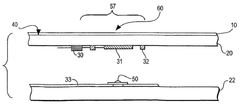
Viewing area 57 represents an area of decorative layer 10 through which light
can pass. Decorative layer 10 may be transparent or translucent at viewing
area 57 or
it may include an aperture (as shown in FIG. 513) aligned with viewing area 57
that
allows light from light emitting diode 50 to pass through at least a portion
of
6
CA 02467553 2010-04-30
r
decorative layer 10 within viewing area 57 to reach the outer surface 60 of
decorative
layer 10 and beyond to a user (not shown). In this embodiment, light emitting
diode
50 is borne on a separate carrier substrate 22 such that electrodes 31 and 32
are
located between separate carrier substrate 22 and substrate 20, although other
configurations are also possible. Separate carrier substrate 22 may be of any
composition and can be composed of the same materials as the substrates
described
above. Also, separate carrier substrate 22 may be decorated according to any
of the
principles of this invention as well. Light emitting diode 50 could be
replaced with
any suitable light source, including a light pipe, incandescent bulb,
electroluminescent
lamp, light emitting polymer, fluorescent light, and so on.
FIGS. 5A and 5C show the embodiment of FIG. 4B, including inner electrode
31, outer electrode 32 and integrated control circuit 30, but with decorative
layer 10
disposed on the non-touched side 140 of substrate 20 instead of on touched
side 40.
FIG. 5B shows an example of decorative layer 10 configured to allow light from
light
emitting diode 50, in FIG. 5C, to reach the surface of touched side 40. In
FIG. 5B,
decorative layer 10 defines an aperture 54 that allows light to reach the
outer surface
40 of decorative layer 10 and beyond to a user (not shown), as illustrated in
FIG. 5C.
FIGS. 6A-7D depict another embodiment of the present invention involving the
novel integrated touch sensor and light emitting device of copending and
commonly owned
U.S. Patent Publication No. 2003/0159910, entitled Integrated Touch Sensor and
Light
Apparatus. Transparent conductive anode layer 51, cathode layer 52 and light
emitting layer
53 of FIG. 6A form the light source and touch pads of the integrated touch
sensor and light
emitting device 56 with integrated control circuit 30 of FIG. 6B. FIG. 6C
shows the touch
sensing components of the integrated touch sensor and light emitting device of
FIG. 6D,
including anode layer 51 coupled to integrated control circuit 30. Substrate
20, having
touched side 40, of FIGS. 6D-6E may be decorated according to the principles
of the present
invention as shown in FIGS. 7A-7B, which show the integrated touch sensor and
light
emitting device 56 with integrated control circuit 30 of FIG. 6B, and as shown
in FIGS. 7C-
7D, which show an integrated touch sensor and light emitting device 56 without
an integrated
control circuit.
7
CA 02467553 2004-05-19
WO 03/044957 PCT/US02/37163
FIGS. 8A-8B show an embodiment of the present invention wherein
decorative layer 10 includes a textured portion 160. Textured portion 160 may
be
disposed in locations on or near touch surface 240 (representing an area where
a
stimulus such as touch or near approach of a human appendage or other object
must
be provided in order to trigger an underlying touch sensor) corresponding to a
particular touch sensor or touch pad to provide a more ergonomic control panel
interface by providing tactile and/or visual feedback to a user who will be
more aware
of the location of the practical boundaries of touch surface 240. Texture of
various
sorts can be achieved using any of the various decorating methods discussed
above as
well as using other techniques. For example, textured portion 160 may be
achieved
through multiple layering of material at certain locations on or near touch
surface 240,
as shown in FIG. 8A, or by incorporating inconsistencies in certain areas of
decorative layer 10, as by stippling, sputter printing, stamping, scoring or
other
methods, as shown in FIG. 8B. FIGS. 8C-8D show an embodiment of the present
invention involving tactile and visual feedback in the form of a dome 65
located
proximate touch surface 240. In such embodiments, the touch sensor underlying
a
dome 65 preferably is configured so as to not be triggered by an appendage,
such as a
finger, simply resting upon the dome, but to be triggered when the dome is
depressed
or "flattened out" against the surface 40 of substrate 20. Dome 65 can be an
integral
part of decorative layer 10, as in FIG. 8C. Alternatively, it can be composed
of
structure 67 separate from decorative layer 10, as shown in FIG. 8D, where
structure
67 is shown both covered by decorative layer 10 and uncovered by decorative
layer
10. Dome 65 may also provide aural feedback in applications where such
feedback
would be advantageous. Aural feedback could be a popping or clicking sound
produced by the transition of the dome between its steady-state dome shape and
a
depressed state.
FIGS. 9A-IOB depict embodiments of the present invention involving back-
lighting using light pipes. The embodiments depicted in these drawings can
involve
touch pads including single electrodes or both inner and outer electrodes, and
can
involve an integrated control circuit proximate the touch pad as well.
The use of light pipes in applications like automotive dashboards, membrane
switches and other electronic applications is common. Light pipes can enhance
the
8
CA 02467553 2010-04-30
legibility and usability of displays on interfaces. Light pipes can be
advantageously
used in conjunction with the principles of the present invention to provide an
improved ergonomic display for touch sensor interfaces.
FIGS. 9A-9C depict embodiments of the present invention wherein substrate
20 is a light pipe. Substrate 20 is advantageously entirely transparent, but
need not
be. Slots 71 can be configured to allow enough light from light source 70 to
illuminate the desired areas at the surface of touched side 40 in embodiments
involving light pipe 171, including embodiments where substrate 20 is not
entirely
transparent. Substrate 20 can include cutout section 72 to accommodate light
source
70. Substrate 21 can include a similar cutout (not shown), as desired.
Alternatively,
light source 70 can be molded directly into substrate 20, as shown in FIG. 9B.
The
embodiment of the present invention shown in FIG. 9B is compatible with the
principles of the invention disclosed in U.S. Patent Publication No.
2003/0159910, entitled
Integrated Touch Sensor and Light Apparatus. Light source 70 can be any
suitable light
emitting component, including, but not limited to, an LED, OLED, LEP, other
electroluminescent device, electroflourescent device or standard incandescent
bulb.
As shown in FIG. 9C, light source 70 emits light that can be refracted by
slots
71 of substrate 20. Slots 71 guide the light emitted from light source 70 to
advantageously provide uniform illumination of an area near or aligned with
electrode
31, as would be understood by those skilled in the art of optics. Slots 71 can
be of
various configurations. In FIG. 9A, the illumination is shown near electrode
31,
where as in FIG. 9B the illumination is shown aligned with electrode 31. Since
light
source 70 can be located in cutout section 72 of substrate 20 or be molded
into
substrate 20, decorative layer 10 in FIG. 9A is shown advantageously disposed
on the
surface of touched side 40. If desired, light source 70 might preferably be
visible at
the surface of touched side 40. In these applications, decorative layer 10 can
be
disposed on non-touched side 140 of substrate 20. Also, both light source 70
and
slots 71 can be covered by a touch pad framing substrate (not shown) atop
substrate
20 that can hide both light source 70 and slots 71, allow decorative layer 10
to be
disposed on the non-touched side 140 of substrate 20 and frame the illuminated
area,
9
CA 02467553 2004-05-19
WO 03/044957 PCT/US02/37163
without needlessly increasing the distance between electrode 31 and the
surface of
touched side 40.
FIGS. IOA-IOB also depict embodiments of the present invention using light
pipes. FIG. I OA shows a touch sensor having a single electrode 31 with an
integrated
decorative layer 10 disposed between light pipe 171 and spacer wedge 120.
Diffuse
reflector 170 reflects light from light source 70 into light pipe 171 where it
can reflect
off of the surface of decorative layer 10 and allow light to reach the touch
sensor user
at the surface of touched side 340. Spacer wedge 120 advantageously keeps
touched
side 340 and electrode 31 parallel. In alternate embodiments, space wedge 120
can be
omitted. Spacer wedge 120, however, advantageously provides an incident angle
to
reflect light better and more uniformly than might be possible without it. In
alternate
embodiments, light can be reflected in a substantially uniform fashion, for
example,
when light pipe 171 is composed of a diffuse material and substrate 20 is
composed of
a reflective material. Light source 70 and electrode 31 can be borne by
substrate 20,
as shown in FIG. 10A, on diffuse reflector 170 and spacer wedge 120,
respectively, or
otherwise. Light source 70 can be any suitable light source, including the
light
sources discussed above. Light source 70 can be configured so that, upon
stimulation
of electrode 31, by a user's touch of touched side 340, light source 70 emits
light
through diffuse reflector 170 and into light pipe 171, providing feedback to
the user
that the touch induced a response in the touch sensor control circuit. Diffuse
reflector
170 can ensure the efficient coupling of light from light source 70, located
adjacent to
light pipe 171, into light pipe 171. Light pipe 171 can ensure the uniform
illumination of touched surface 40. Alternately, light pipe 171 could be
integrated
with an optical switching mechanism. For instance, an infrared detector (not
shown)
could detect the inherent body heat of a user's touch through light pipe 171.
Or an
emitter-detector pair (not shown) could detect the shadow of a user's
approaching
touch through light pipe 171. It will be understood that light pipe 171 could
be any
suitable optical device, including a waveguide or a lens. FIG. I OB shows a
possible
configuration of integrated touch sensors according to the present invention.
In FIG.
1013, triangular spacer wedges 120 overlie complementary electrodes 31. When
the
configuration defined by diffuse reflector 170 and light pipe 171 overlies
associated
spacer wedge 120, diffuse reflector 170 aligns with light source 70, as shown
in FIG.
I OA. Decorative layer 10 can advantageously differentiate among touch sensors
by
CA 02467553 2004-05-19
WO 03/044957 PCT/US02/37163
changing the color of light from light source 70. Alternately, lights 70 could
emit
different wavelengths of light for each separate touch sensor.
FIGS. 11A-11B depict other embodiments of the present invention that
include light pipes. In FIG. 1 1A, electrodes 31 and 32 and light emitting
device 50
are borne on substrate 20. Light pipe 171 is also borne on substrate 20 and
can be
dispensed, molded and the like. Decorative layer 10 is disposed atop
electrodes 31
and 32. Light pipe 171 may be cured using thermal or ultraviolet techniques,
or the
like, to conform to the electrodes 31 and 32 and light emitting device 50
borne on
substrate 20. Also shown in FIG. 11A is a second decorative layer 110,
disposed atop
light pipe 171. In FIG. 11A, second decorative layer 110 is shown having
section
154, which can be transparent or translucent to allow light from light
emitting device
50 to reach touched side 40. Section 154 is optional and in alternate
embodiments can
be obviated when second decorative layer 110 includes an aperture (not shown)
as
described with reference to FIGS. 5B and 5C. The embodiments depicted in FIG.
11A also advantageously have raised surface 440, which can alert a touch
sensor user
to the presence of an operative touch surface in a manner similar to the
textured areas
and domes of FIGS. 8A-8D. FIG. 11B shows a similar embodiment of the present
invention where electrodes 31 and 32, light emitting device 50 and integrated
control
circuit 30 are borne on the opposite, non-touched side 140 of substrate 20. In
these
configurations, light from light emitting device 50 must first pass through
substrate 20
before reaching light pipe 171, which illuminates section 154. The embodiment
in
FIG. 11B advantageously allows light pipe 171 to be borne on substrate 20
without
having to conform to electrodes 31 and 32, light emitting device 50 or other
components. In FIGS. 11A-11B, light emitting device could be mounted on
substrate
20 using wire-bonding, flip chip or other direct die attachment methods in
addition to
using standard surface mount packaging of plastic encapsulated parts on either
side of
substrate 20. The light pipes 171 and other components of these configurations
could
also be decorated according to the principles of the present invention as
described
above. Although in FIGS. 11A and 1 lB light pipe 171 is shown nearer touched
side
40, light pipe 171 can also be advantageously be borne on non-touched side 140
of
substrate 20.
11
CA 02467553 2010-04-30
Although the touch sensors herein are shown having inner and outer
electrodes, the inner or outer electrode can be eliminated in some
embodiments.
Moreover, the present invention can be used with any type of touch sensor,
including
capacitive touch sensors or touch switches with integrated control circuits.
The
principles of the present invention are also compatible with the inventions of
other
commonly owned and assigned applications. For instance, a touch sensor with an
integrated decorative substrate can involve the novel circuitry of U.S. Patent
No. 7,242,393
and also can include the integrated lighting of the invention disclosed in
U.S. Patent
Publication No. 2003/0159910. Moreover, a touch sensor with an integrated
decorative
substrate can also include substrates that are thermoformed or injection
molded onto the
decorated substrates according to the invention disclosed in U. S. Patent No.
6,897,390,
entitled Molded/Integrated Touch Switch/Control Panel Assembly and Method for
Making
Same.
The preceding drawings serve to illustrate, but neither limit nor exhaust, the
principles of the present invention. Various alterations to the embodiments
described
above are in keeping with the spirit of the invention and will be understood
by those
skilled in the art to be a part of the present invention claimed below.
12