Note: Descriptions are shown in the official language in which they were submitted.
CA 02467713 2004-05-18
WO 03/015866 PCT/US02/26590
1
APPARATUS AND METHOD FOR BIOELECTRIC STIMULATION,
HEALING ACCELERATION AND PAIN RELIEF
TECHNICAL FIELD OF THE INVENTION
The present invention relates to a pulsed signal generator for biomedical
applications.
In particular, the present invention relates to a light-weight, compact pulsed
signal generator
that produces an output waveform based on at least four timing intervals
T1¨T4, more
preferably, a waveform based on seven timing intervals T1¨T7.
BACKGROUND ART
Injuries, infections and degenerative conditions are major sources of pain,
inconvenience, expense, lost work (and leisure) time and diminished
productivity. The
problems associated with these conditions grow worse with age, since an injury
which would
heal quickly in a young, healthy person takes much longer in one who is older,
in poor
health, or both. In demographically-aging societies such as now seen in most
of the
industrialized nations, these social and economic impacts will become
increasingly magnified
over the course of the next several decades.
While it is difficult to estimate the total cost of such conditions¨leaving
aside their
impact on quality of life¨the total surely amounts to many billions of dollars
per year in the
United States alone. For example, between five and ten million United States
residents suffer
broken bones every year, with many of these cases involving multiple
fractures. In a young,
healthy patient, many fractures need to be immobilized in a cast for six weeks
or more. Even
after the cast is removed, the patient's activities are frequently restricted
until the healed bone
regains its full strength. In the elderly, in persons with poor health or
malnutrition, in
patients with multiple fractures, or in patients with conditions that impact
healing processes,
fractures heal more slowly. In some cases, the fractures do not heal at all,
resulting in the
conditions known as "nonunion" or "nonunion fracture" which sometimes persists
for a
lifetime.
As a result, an estimated quarter-million person-years of productivity are
lost in the
United States due to bone fractures alone. Similar statistics can be generated
not only for
other classes of traumatic injury, but also for chronic conditions such as
osteoarthritis,
osteoporosis, diabetic and decubitus ulcers, damaged ligaments, tendonitis,
and repetitive
stress injuries (including the conditions commonly known as "tennis elbow" and
carpal tunnel
syndrome).
Since the 1960s, it has been increasingly recognized that the human body
generates a
host of low-level electric signals as a result of injury, stress and other
factors; that these
CA 02467713 2004-05-18
WO 03/015866 PCT/US02/26590
9
signals play a necessary part in healing and disease-recovery processes; and
that such
processes can be accelerated by providing artificially-generated signals which
mimic the
body's own in frequency, waveform and strength. Such "mimic" signals have been
shown
to have many effects in the body, including helping to direct mobile cells
such as fibroblasts
and macrophages to sites where they are needed (galvanotaxis) and causing the
release of cell
growth factors such as transforming growth factor beta (TGF-(i) and insulin-
like growth
factor (IGF). The results can include more rapid healing of skin and muscle
wounds,
including chronic ulcers such as those resulting from diabetes; the mending of
broken bones,
including most nonunion fractures; the regrowth of injured or severed nerves;
and the repair
of tissues damaged by repetitive motion, as in tendonitis and osteoarthritis;
and the reduction
of swelling, inflammation, and pain, including chronic pain for which the
usual drug-based
treatments do not bring satisfactory relief.
Some of the body's signals, such as the "injury potential" or "current of
injury"
measured in wounds, are DC (direct current) only, changing slowly with time.
It has been
found that bone fracture repair and nerve regrowth are typically faster than
usual in the
vicinity of a negative electrode but slower near a positive one, where in some
cases tissue
atrophy or necrosis may occur. For this reason, most recent research has
focused on higher-
frequency, more complex signals often with no net DC component.
While most complex-signal studies to date have been performed on bone fracture
healing, the commonality of basic physiological processes in all tissues
suggests that the
appropriate signals will be effective in accelerating many other healing and
disease-recovery
processes. Indeed, specific frequency and waveform combinations have been
observed to
combat osteoarthritis and insomnia, stimulate hair growth, reduce swelling and
inflammation,
fight localized infection, speed the healing of injured soft tissues including
skin, nerves,
ligaments and tendons, and relieve pain without the substituted discomfort of
TENS
(transcutaneous electric nerve stimulation).
Figs. IA and 1B show a schematic view of a waveform 20 which has been found
effective in stimulating bone fracture healing, where a line 22 (Fig. 1A)
represents the
waveform on a short time scale, a line 24 (Fig. 1 B) represents the same
waveform on a
longer time scale, levels 26 and 28 represent two different characteristic
values of voltage or
current, and intervals 30, 32, 34 and 36 represent the timing between specific
transitions.
Levels 26 and 28 are usually selected so that, when averaged over a full cycle
of the
waveform, there is no net DC component. In real-world applications, waveform
20 is
typically modified in that all voltages or currents decay exponentially toward
some
intermediate level between levels 26 and 28, with a decay time constant
usually on the order
of interval 34. The result is represented by a line 38 (Fig. IC).
In a typical commercially-available device for treating fracture nonunions,
interval 30
is about 200 pec, interval 32 about 30 [isec, interval 34 about 5 msec, and
interval 36 about
60 msec. Alternate repetition of intervals 30 and 32 generates pulse bursts
40, each of the
CA 02467713 2004-05-18
WO 03/015866 PCT/US02/26590
3
length of interval 34, separated by intervals of length 36 in which the signal
remains
approximately at level 28. Each waveform 38 thus consists of rectangular waves
alternating
between levels 26 and 28 at a frequency of about 4400 Hz and a duty cycle of
about 85%.
The pulse bursts are repeated at a frequency of about 15 Hz and a duty cycle
of about 7.5%,
alternating with periods of substantially no signal. The timing of such a
signal can vary
broadly, since the characteristics of signals generated by bone in vivo and in
vitro depend on
a number of factors, including but not necessarily limited to its type, size
and mineral density,
and the amount of stress and its rate of application. Hence, osteoblasts are
believed to be able
to respond to a range of signals which differ somewhat in waveform and
frequency content.
However, tissues may respond differently to markedly different frequencies and
waveforms. For example, the waveform of Figs. 1A¨C is effective in speeding
the healing
of a bone fracture but much less so in slowing the progress of osteoporosis.
On the other
hand, a waveform 50 (Fig. 2) consisting of single pulses 52 of polarity 26
lasting
approximately 350-400 [Asec each, alternating with intervals 54 of polarity 28
at a frequency
of approximately 60-75 Hz, can slow or even reverse osteoporosis but has
little effect on
fracture repair. Again, the exact waveform and frequency for each application
may vary.
The signal intensity may also vary; indeed, more powerful signals often give
no more
benefit than weaker ones, and sometimes less. This paradoxical relationship is
shown
schematically in Fig. 3, where a line 60 represents the magnitude of the
healing effect a
various signal intensities. For a typical signal (such as the signal of Figs.
1A¨C), a peak
effectiveness 62 typically falls somewhere between one and ten 1,1A/cm2, and a
crossover
point 64 at about a hundred times this value. Beyond point 64, the signal may
slow healing
or may itself cause further injury. Similar responses are seen in other
biological processes
that are responsive to electrical stimulation, including cell division,
protein and DNA
synthesis, gene expression, and intracellular second-messenger concentrations.
For example,
while conventional TENS can block pain perception with a relatively strong
signal, much as a
jamming signal blocks radio communication, it can also lead to progressively
worsening
injury since the pain's warning function has also been defeated.
The important factors for most .healing applications appears to be that the
high-
frequency signal appears in bursts, separated by intervals of quiet or no
signal, and that the
waveform within these bursts is itself asymmetric. Results appear to be better
when
frequency components above about 50 KHz are filtered out, giving transition
times on the
order of five isec. Tests using sine waves, square waves, frequencies above
about 50 KHz,
or waveforms generally resembling that in Fig. 1 but with duty cycles
approaching 50% or
with excessively fast or slow rise times, have shown much lower effectiveness
at otherwise-
comparable power levels.
CA 02467713 2004-05-18
WO 03/015866 PCT/US02/26590
4
Many different types of electrical stimulation devices are available to
consumers and
medical professionals, producing many different waveforms ranging from
constant-current or
constant voltage (DC) through low-frequency to high frequency waveforms. In
general, the
lower-frequency waveforms and high-frequency pulses within a low-frequency
envelope tend
to be aimed at tissue-healing applications, while higher-frequency waveforms
are used for
pain relief.
Electrical stimulation is widely used in tissue healing applications. Here,
Petrofsky
(U.S. No. 5,974,342) shows a microprocessor-controlled apparatus for treating
injured =
tissue, tendon, or muscle by applying a therapeutic current. The apparatus has
several
channels that provide biphasic constant voltage or current, including a 100-
300 Asec positive
phase, a 200-750 !Asec interphase, and a 100-300 psec negative phase occurring
once every
12.5-25 msec.
Pilla, et al. (U.S. No. 5,723,001) disclose an apparatus for therapeutically
treating
human body tissue with pulsed radio-frequency electromagnetic radiation. The
apparatus
generates bursts of pulses having a frequency of 1-100 MHz, with 100-100,000
pulses per
burst, and a burst repetition rate of 0.01-1000 Hz. The pulse envelope can be
regular,
irregular, or random.
Bartell, et al. (U.S. 5,117,826) discloses an apparatus and method for
combined
nerve fiber and body tissue stimulation. The apparatus generates biphasic
pulse pairs for
nerve fiber stimulation, and a net DC stimulus for body tissue treatment
(provided by biphasic
pulse trains having a greater number of negative than positive pulses). In
U.S. No.
4,895,154, Bartell, et al. describe a device for stimulating enhanced healing
of soft tissue
wounds that includes a plurality of signal generators for generating output
pulses. The
intensity, polarity, and rate of the output pulses can be varied via a series
of control knobs or
switches on the front panel of the device.
Gu, et al. (U.S. No. 5,018,525) show an apparatus that generates a pulse train
made
up of bursts having the same width, where each burst is made up of a plurality
of pulses of a
specific frequency. The number of pulses varies from one burst to the next;
the frequency of
the pulses in each burst varies from one burst to the next corresponding to
the variation in the
number of pulses in each burst. The pulses have a frequency of 230-280 KHz;
the duty
cycle of the bursts is between 0.33% and 5.0%.
Liss, et al. (U.S. No. 5,109,847) relates to a portable, non-invasive
electronic
apparatus which generates a specifically contoured constant current and
current-limited
waveform including a carrier frequency with at least two low-frequency
modulations. The
carrier frequency is between 1-100,000 KHz; square-wave or rectangular-wave
modulating
frequencies are 0.01-199 KHz and 0.1-100 KHz. Duty cycles may vary, but are
typically
50%, 50%, and 75% for the three waveforms.
CA 02467713 2015-08-24
Borkan's tissue stimulator (U.S. No. 4,612,934) includes an implantable,
subcutaneous receiver and implantable electrodes. The receiver can be
Doninvasively
programmed after implantation to stimulate different electrodes or change
stimulation
parameters (polarity and pulse parameters) in order to achieve the desired
response; the
5 programming data is transmitted in the form of a modulated signal on a
carrier wave. The
programmed stimulus can be modified in response to measured physiological
parameters and
electrode impedance.
Hondeghem (U.S. No. 4,255,790) describes a programmable pulse generating
system where the time periods and sub-intervals of the output pulses are
defined by signals
from a fundamental clock frequency generation circuit, plus a pair of parallel
sets of
frequency division circuits connected to that circuit. The time periods, sub-
intervals, and
output waveforms are variable.
Hsiang-Lai, et al. (U.S. No. 3,946,745) provide an apparatus for generating
positive
and negative electric pulses for therapeutic purposes. The apparatus generates
a signal
consisting of successive pairs of pulses, where the pulses of each pair are of
opposite
polarities. The amplitude, duration, the interval between the pulses of each
pair, and the
interval between suecessive pairs of pulses are independently variable.
McDonald (U.S. No. 3,589,370) shows an electronic muscle stimulator which
produces bursts of bidirectional pulses by applying unidirectional pulses to a
suitable
transformer.
Landauer (U.S. No. 3,294,092) discloses an apparatus that produces electrical
currents for counteracting muscle atrophy, defects due to poor nutrition,
removing exudates,
and minimizing the formation of adhesions. The amplitude of the output signals
is variable. =
Kronberg (U.S. No. 5,217,009, No. 5,413,596, U.S. No. 6,011,994, U.S. No.
6,321,119) describes signal generators for biomedical applications. The
generators produce pulsed signals having fixed and variable amplitude,
fixed, variable, and swept frequencies, and (in some cases) optional DC
biasing.
Units designed for use in transcutaneous electroneural stimulation ("TENS")
for pain
relief are widely available. For example, Bastyr, et al. (U.S. No. 5,487,759)
disclose a
battery-powered device that can be used with different types of support
devices that hold the
electrode pads in position. Keyed connectors provide a binary code that is
used to determine
what type of support device is being used for impedance matching and carrier
frequency
adjustment. The carrier frequency is about 2.5-3.0 KHz; the therapeutic
frequency is
typically on the order of 2-100 Hz.
Kolen (U.S. No. 5,350,414) provides a device where the carrier pulse
frequency,
modulation pulse frequency, intensity, and frequency/amplitude modulation are
controlled by
a microprocessor. The device includes a pulse modulation scheme where the
carrier
CA 02467713 2004-05-18
WO 03/015866 PCT/US02/26590
6
frequency is matched to the electrode-tissue load at the treatment site to
provide more efficient
energy transfer.
Liss, et al. (U.S. No. 4,784,142) discloses an electronic dental analgesia
apparatus
and method. The apparatus generates a output with relatively high frequency
(12-20 KHz)
pulses with nonsymmetrical low frequency (8-20 Hz) amplitude modulation.
Bartelt, et al. (U.S. No. 5,063,929) describe a microprocessor-controlled
device that
generates biphasic constant-current output pulses. The stimulus intensity can
be varied by the
user.
Charters, et al. (U.S. No.. 4,938,223) provide a device with an output signal
consisting of bursts of stimuli with waxing and waning amplitudes, where the
amplitude of
each stimulus is a fixed percentage of the amplitude of the burst. The signal
is amplitude-
modulated to help prevent the adaptation response in patients.
Molina-Negro, et al. (U.S. No. 4,541,432) disclose an electric nerve
stimulation
device for pain relief. The device produces a bipolar rectangular signal with
a preselected
repetition rate and width for a first time period. Then, a rectangular signal
is generated at a
pseudo-random rate for a second time period, and delivery of the signal is
inhibited for a
third, pseudo-random period of time. This protocol is said to substantially
eliminate
adaptation of nerve cells to the stimulation.
Butler, et al. (U.S. No. 4,431,000) show a transcutaneous nerve stimulator for
treating aphasias and other neurologically-based speech and language
impairments. The
device uses a pseudorandom pulse generator to produce an irregular pulse train
composed of
trapezoidal, monophasic pulses which mimic typical physiological wave forms
(such as the
brain alpha rhythm). A series of such pulses has a zero DC level; a current
source in the
device reduces the effects of variables such as skin resistance.
Maurer (U.S. No. 4,340,063) discloses a stimulation device which can be
implanted
or applied to the body surface. The amplitude of the pulse decreases with a
degradation in
pulse width along a curve defined by a hyperbolic strength-duration curve.
This is said to
result in proportionately greater recruitment of nerve fibers due to the
nonlinear relationship
between pulse width and threshold.
The Kosugi, et al. system (U.S. No. 4,338,945) generates pulses that fluctuate
in
accordance with the 1/f rule. That is, the spectral density of the fluctuation
varies inversely
with the frequency: pleasant stimuli often have stochastic fluctuations
governed by this rule.
The system produces an irregular pulse train said to promote patient comfort
during the
stimulation.
Signal generators are also used in hearing prostheses. For example,
McDermott's
receiver/stimulator (U.S. No. 4,947,8/1/1) generates a series of short spaced
current pulses,
with between-pulse intervals of zero current having a duration longer than
that of each spaced
pulse. The waveform of the stimulus current includes a series of these spaced
pulses of one
CA 02467713 2015-08-24
7
polarity followed by an equal number of spaced pulses of opposite polarity so
that the sum of
electrical charge transferred through the electrodes is approximately zero.
Alloca (U.S. No. 4,754,7590 describes a neural conduction accelerator for
generating
a train of "staircase-shaped" pulses whose peak negative amplitude is two-
thirds of the peak
positive amplitude. The accelerator design is based on Fourier analysis of
nerve action
potentials; the output frequency can be varied between 1-1000 Hz.
Galbraith (U.S. No. 4,592,359) describes a multi-channel implantable neural
stimulator wherein each data channel is adapted to carry information in
monopolar, bipolar, or
analog form. The device includes charge balance switches designed to recover
residual
charge when the current sources are turned off (electrode damage and bone
growth are said to
be prevented by not passing DC current or charge).
Despite its great healing potential, traditional Western medicine has accepted
electrotherapeutic treatment only grudgingly, and to date it is used only
rarely. This seems to
be a legacy from early beliefs that signals would need to have high local
intensities to be
effective. Most electrotherapeutic apparatus now available relies either on
direct implantation
of electrodes or entire electronic packages, or on inductive coupling through
the skin. The
need for surgery and biocompatible materials in the one case, and excessive
circuit complexity
and input power in the other, has kept the price of most such apparatus (apart
from TENS
devices) relatively high, and has also restricted its application to highly
trained personnel.
There remains a need for a versatile, cost-effective apparatus that can be
used to provide
bioelectric stimulation in a wide range of applications, including healing
acceleration and pain
relief.
DISCLOSURE OF THE INVENTION
According to its major aspects and broadly stated, the present invention is an
apparatus and method for generating an electrical signal for use in biomedical
applications.
The signal includes an asymmetrical, biphasic wave form consisting of
intermittent bursts of
quasi-rectangular waves, based on at least four timing intervals T1¨T4; more
preferably, the
signal is based on seven timing intervals T1¨T7. The apparatus includes a
first timing block
for generating timing intervals T1 and T2; a second timing block for
generating timing intervals
T3 and 1'4 (the timing blocks also generate intervals T5, T6, and T7 if
present); an
interconnection block for combining these intervals into an output signal
having
predetermined relationships among the intervals; an output block for
transmitting the output
signal to a load (such as tissue being treated with the apparatus); a battery
pack; and,
optionally, a filter for removing unwanted frequency components from the
output signal; and
an adjustment block for selecting from among a plurality of output signals
with predetermined
characteristics. The signal has a first amplitude level LI during intervals
T1, T5, and T6, a
second level L., during intervals T2 and T4, and a third level Ls during
interval 1'
7, where L-
falls in the range between L1 and L2, inclusive.
CA 02467713 2004-05-18
WO 03/015866 PCT/US02/26590
8
The apparatus is lightweight, compact, self-contained, cost-effective to
manufacture
and maintain, and convenient to carry or wear for extended periods. It is safe
for
unsupervised home use without the need for special training, and able to
generate the above-
described output signal and deliver it efficiently through conductive pads
making direct
contact with the load. Since only low voltages and currents are used, the
apparatus does not
pose a shock hazard even in case of malfunction. Power is furnished by compact
and
inexpensive batteries, needing replacement only once in several weeks of use.
The apparatus may be used to provide in vivo, customizable electrotherapeutic
treatment for human and animal patients, including but not necessarily limited
to healing
acceleration, relief of acute or chronic pain, and relief of swelling and/or
inflammation. Since
isolated cells or tissue cultures can also be affected by electrotherapeutic
waveforms
(appropriate electrical stimuli have been observed to modify the rates of cell
metabolism,
secretion, and replication), the apparatus may also be used for in vitro
applications. In
contrast to TENS-type devices, which are aimed at blocking pain impulses in
the nervous
system, the apparatus operates at a signal level which is below the normal
human threshold
level: most users do not experience any sensation during treatment apart from
a steady
decrease in previously existing pain. The apparatus is believed to operate
directly at the
treatment site by enhancing the release of chemical factors such as cytokines
which are
involved in cellular responses to various physiological conditions. This
results in increased ,
blood flow and inhibits further inflammation at the treatment site, thereby
enhancing the
body's inherent healing processes.
The output signal is an important feature of the present invention. The output
signal is
a waveform based on at least four timing intervals T1¨T4 having the following
relationships:
(a) (2 x T2) s T1 s (20 x T2)
(b) 50 Asec s (T1 + T2) s 5000 vsec
(c) T3 (10 X TO
(d) T4 500 msec
where the signal has a first amplitude level L1 during interval T1 and a
second amplitude level
L2 during intervals T2 and T4, where intervals T1 and T2 alternate through
interval T3, and
where intervals T3 and T4 also alternate.
More preferably, the waveform is based on seven timing intervals T1¨T7, with
three
different amplitude levels as described above. The timing intervals have,
approximately, the
following relationships:
(a) (2 x T2) s Ti s (20 x T2)
(b) 50tAsec (ri + T2) 5000 lAsec
(c) T3 (10 X TO
(d) 0 s T4 500 msec
CA 02467713 2004-05-18
WO 03/015866 PCT/US02/26590
9
(e) 0 T5 Ti
(f) 0 T6 T1
(g) 0 500 msec
(h) 5 msec (T3 + T4 + T7) 500 msec
In a preferred embodiment of the invention, interval T3 includes the following
sequence: an
interval T5, followed by at least one pair of intervals (T'1, T2) and then by
an interval T6. The
timing intervals and amplitude levels are variable, providing an output signal
that can be
adjusted for a wide range of therapeutic applications.
The apparatus for generating the signal is another important feature of the
present
invention. The apparatus includes timing blocks (such as oscillators or
astable multivibrators)
for generating the timing intervals, preferably connected so that the first
timing block controls
the second timing block through the interconnection block. The apparatus may
include a
switching block that enables the user to select from among a plurality of
paired values of
intervals (T1, T2), a plurality of paired values of intervals (T3, T4), and a
plurality of
amplitude output levels L1¨L3. More preferably, the transition between any two
of levels L1
through L3 has a decay time constant no greater than approximately 1/2 T2. If
desired, the
apparatus may produce a waveform wherein all amplitude levels decay towards a
value L4
intermediate between L1 and L2. In this case, L4 may or may not be equal to
L3, and the
decay takes place with a time constant no less than approximately 10 times T1.
Thus, the
output signal is adjustable in both waveform and amplitude to suit the needs
of the individual
user and the particular application.
Another feature of the present invention is the provision of interval T7,
during which
intermediate voltage or current level L3 is presented to the load rather than
low level L. This
feature minimizes the amount of energy which is presented to the load (such as
tissue being
treated with the apparatus) during this resting interval between pulse
bursts..
Still another feature of the present invention is the filter, which blocks
frequencies
above a selected level (i.e., frequencies greater than the highest ones
intentionally generated),
to create a desired transition profile or to prevent interference by external
high-frequency
signal sources. For example, the filter may include a shunt capacitance, a
resistor network, a
voltage-controlled current source, or other suitable device that
simultaneously slows and
controls the rate of transitions, attenuates output frequency components above
about 50 KHz
(or other selected frequency), and prevents interference with circuit
functioning by external
radio-frequency signals.
Yet another feature of the present invention is the use of dual timing blocks
to generate
waveforms that can be combined to produce an output waveform having selected
characteristics. In a preferred embodiment of the invention, one of two timing
blocks is
controlled by the other: that is, the output of the second block is "on" or
"off" depending on
whether the output of the first block is "low" or "high," respectively. This
results in a circuit
CA 02467713 2013-08-19
that generates an output signal whose characteristics¨frequency, duty cycle,
amplitude¨can
be determined over a wide range by the particular selection of components. Two
such circuits
with output signals having appropriately-selected characteristics can be
combined to produce
the desired output waveform, with timing intervals Ti through T7, with a
surprisingly simple
5 overall circuit configuration.
Another feature of the present invention is the use of conventional, readily-
available
low-voltage batteries as a power source for the apparatus. While the invention
may be used
with AC (alternating current) power sources (with the addition of any suitable
adapter),
battery power not only reduces the size and weight of the apparatus, but also
adds to its safety
10 and ease of use for a patient undergoing treatment. Typically, the
batteries need to be
replaced at infrequent intervals (generally no more than once every few weeks,
depending on
the output signal and the particular application), simplifying patient
compliance and reducing
operating costs. The possibility of electrical injuries is greatly reduced,
since the generator is
not connected to AC line current during use, does not produce high voltages,
and does not
generate frequencies likely to induce ventricular fibrillation. Only low power
levels, such as
are required to produce therapeutic effects, are applied to the body. Thus,
the generator
cannot produce an electrical shock hazard even in the event of a malfunction:
as a result, the
invention is suitable for unsupervised home use.
=
Still another feature of the present invention is its versatility. The
components of the
apparatus are selected so as to produce an output waveform with selectable
timing intervals T1
through T7 and output voltage (or current) levels L1 through 1,3. As noted
above, tissues may
respond in different ways to different signal frequencies, to a pure AC
signal, or to an AC
signal with a superimposed positive or negative DC component Similarly, as
shown in Fig.
3, different effects may appear at different current densities.
An apparatus with an adjustable output signal is useful for a greater variety
of
applications than one having a fixed output; on the other hand, medical
professionals may
prefer a generator having a fixed output, or an output that is adjustable only
in magnitude, for
outpatient use by their patients. In one embodiment of the invention, the user
can select a
signal for a given application by turning a dial or using a keypad to select
one of a plurality of
the available signals noted above.
Yet another feature of the present invention is the ability to turn off the
output signal
after a predetermined treatment duration, to reverse the polarity of the
signal at predetermined
intervals, or both. An optional timing device allows the user to thereby
customize the
treatment for the individual patient.
CA 02467713 2013-08-19
10a
The invention in one broad aspect pertains to an apparatus for use in
biomedical
application, the apparatus comprising means for generating a set of at least
four timing intervals
T1-T4, the timing intervals T3-T4 forming a longer cycle including at least
one pulse bursts
occurring in the timing interval T3, the pulse burst having pulses of a first
polarity with a first
duration equal to the timing interval T1 alternating with pulses of a second
polarity with a second
duration equal to the timing interval T2. The pulse burst is followed by an
equalizing pulse of a
third polarity and duration equal to the time interval 14 to neutralize an
accumulated charge
resulting from a difference between timing intervals Ti and T2 before a next
successive pulse
burst. The timing intervals T1-T4 having approximately the relationships
(a) (2 x T2) T1 5_ (20 x T2).
(b) 50 sec (Ti + T2) 5000 sec,
(c) T3 (10 x T1), and
(d) 0 T4 500 msec; and
means for using the timing intervals to generate an electrical signal having
an
amplitude.
Another aspect of the invention provides an apparatus for generating an
electrical
signal including at least four timing intervals 11-14, the apparatus
comprising a first timing block
for generating a first timing interval T1 and a second timing interval 12, a
second timing block
for generating a third timing interval 13 and a fourth timing interval 14. The
timing intervals 13-
T4 form a longer cycle including at least one pulse bursts occurring in the
timing interval 13, the
pulse burst having pulses of a first polarity with a first duration equal to
the timing interval Ti
alternating with pulses of a second polarity with a second duration equal to
the timing interval
12. The pulse burst is followed by an equalizing pulse of a third polarity and
duration equal to
the time interval T4 to neutralize an accumulated charge resulting from a
difference between
CA 02467713 2013-08-19
10b
timing intervals Ti and T2 before a next successive pulse burst. The intervals
Ti- T4 having
approximately the relationships
(a) (2 x T2) 5 11 < (20 x T2),
(b) 50 sec (T1+ 12) 5000 sec,
(c) 13 > (10 X Ti). and
(d) 0 < T4 < 500 msec
An interconnection block is operably connected between the first and second
timing blocks, the interconnection block combining the intervals T1-T4, and
means is operably
connected to the interconnection block for using the timing intervals to
generate an output signal
with the intervals 11-14.
Still further, the invention provides a method for generating an electrical
signal,
the method comprising generating at least four timing intervals Ti-T4 having
approximately the
relationships
(a) (2 x 12) < Ti <(20 x 12),
(b) 50 sec < (T1 + 12) < 5000 sec,
(c) 13 > (10 X Ti), and
(d) 0 < T4 < 500 msec; and
using the timing intervals to generate an electrical signal.
Other features and advantages of the present invention will be apparent to
those skilled in
the art from a careful reading of the Best Modes for Carrying out the
Invention presented below
and accompanied by the drawings.
BRIEF DESCRIPTION OF THE DRAWINGS
CA 02467713 2004-05-18
WO 03/015866 PCT/US02/26590
11
In the drawings,
Figs. 1A and 1B are schematic views of a waveform used in stimulating fracture
healing, on a short and a long time scale, respectively;
Fig. IC shows a modified form of the waveform of Fig. 1B;
Fig. 2 shows a waveform used in the treatment of osteoporosis;
Fig. 3 is a schematic view of healing effect vs. signal intensity (amplitude);
Fig. 4 illustrates a waveform according to a preferred embodiment of the
present
invention;
Figs. 5A¨F illustrates specific embodiments of the waveform of Fig. 4;
Fig. 6 is a block diagram of an apparatus according to a preferred embodiment
of the
present invention;
Fig. 7 and 8 show an asymmetric oscillator circuit and a dual asymmetric
oscillator
circuit, respectively, both being usable with the apparatus of Fig. 6;
Fig. 9 shows a plurality of waveforms output by a particular embodiment of the
apparatus of Fig. 6;
Figs. 10, 11, and 12 show a power supply, a pair of timing blocks, and a
voltage
switching block and filter with associated circuitry, respectively, all being
usable with the
apparatus of Fig. 6;
Fig. 13 is a schematic view of a pair of output waveforms;
Fig. 14 illustrates a waveform wherein the voltage levels are adjusted so as
to produce
a strong direct current (DC) signal component;
Fig. 15 shows an alternative form of the circuitry of Fig. 12, designed for
generation
of the signal of Fig. 14;
Fig. 16A and 16B illustrate a waveform with a DC component which is reversed
in
polarity at selected intervals;
Fig. 17 illustrates a waveform with a DC component and periodically reversed
polarity which is also turned off after a preselected length of treatment; and
Fig. 18 shows an alternative form of the circuit of Figure 11, designed for
generation
of waveforms such as those of Figs. 15 and 16.
BEST MODES FOR CARRYING OUT THE INVENTION
In the following description of best modes for carrying out the invention,
reference
numerals are used to identify structural elements, portions of elements,
surfaces or areas in
the drawings, as such elements, portions, surfaces or areas may be further
described or
explained by the entire written specification. For consistency, whenever the
same numeral is
used in different drawings, it indicates the same element, portion, surface or
area as when
first used. Unless otherwise indicated, the drawings are intended to be read
together with the
specification, and are to be considered a portion of the entire written
description of this
CA 02467713 2015-08-24
12
invention. As used herein, the terms "horizontal," "vertical,"
"left," right," "up," "down," as well as adjectival and adverbial derivatives
thereof, refer to
the relative orientation of the illustrated structure as the particular
drawing figure faces the
reader.
The present invention is an apparatus for use in providing bioelectric
stimulation in a
variety of applications. The apparatus generates a waveform having
approximately
rectangular or quasirectangular, asymmetric pulses repeated at a chosen
frequency below
approximately 50 KHz, with frequencies above approximately 50 KHz filtered out
(however,
different cut-off frequencies may also be useful). These pulses appear in
bursts which
themselves are repeated at a lower frequency. The characteristics of the
waveform are
variable to suit differing applications or target tissues to be treated, as
will be described
further below.
Referring now to Fig. 4, there is shown a waveform 70 according to a preferred
embodiment of the present invention. Waveform 70, indicated by line 72, has
seven timing
intervals T1¨T7, indicated as intervals 74a-74g, respectively, and three
levels of voltage or
current L1¨L3, indicated as levels 76a-76c. While level L1 is shown as being
above L2 in
Fig. 4, it should be understood that LI is not necessarily either positive or
negative with
respect to L2. Intervals T1¨T7 are related as follows:
(a) (2 x T2) s Ti s (20 x T2)
(b) 50 [Asec (r, + T2) 5000 sec
(c) T3 (10 X TO
(d) 0 .s T4 500 msec
(e) 0 T5 s Ti
(f) 0 s T6 T1
(g) 0 s s 500 msec
(h) 5 msec _s (T3 + + s 500 msec
That is, interval 74a (T1) is between 2-20 times, preferably about seven
times, as long
as interval 74b (1'2), corresponding to duty cycles between about 5% and 33%.
The sum of
T1 and T2 lies in the approximate range of 50-5000 pee. Intervals 74e (T5) and
74f (16)
range from zero to T1 in length. Interval 74c (T3) is at least approximately
ten times interval
74a (1,). The sum of 74c (1,), 74d (14) and 74g (T7) lies in the range from 5
msec to 500
msec, and is preferably about 70 msec. (It should be understood that these
ranges are
approximate; values of T1¨T7 outside these ranges may also be useful.) Subject
to these
constraints, any one or combination of T4, 16, T6, and T7 may each have any
length,
including zero.
Intervals Ti and T2 form an alternating cycle To T2, T1, T2 and so forth,
representing
opposite phases of a rectangular wave whose frequency lies in the range from
about 200
Hz-201(Hz. Similarly, intervals T3, T4, and T7 form an alternating cycle T3,
T4,17, T3, T4,
CA 02467713 2015-08-24
13
T7 and so forth, representing successive phases in a three-phase wave whose
frequency lies
between approximately 5-50 Hz. Each interval T3 is subdivided into a plurality
of shorter
intervals beginning with a single interval T5, proceeding through a plurality
of intervals T1
and T2 alternating as described above, and ending with a single interval T6
whose end
coincides with that of interval 1'3, so that a representative (if atypically
short) example might
be T5, To 1'2, T1, T2, T6. Intervals T4 and T7, in contrast, are not so
subdivided.
First and second levels L1 (level 76a) and L, (level 76b) of voltage or
current are
opposite in polarity and define a range between them which, within tissue
undergoing
treatment with waveform 70, typically spans a few mV/cm (voltage) or a few
pA/cm2
(current). Within this range lie a third and optionally a fourth voltage or
current level 1,3 (level
76) and L4 (level 76e), either of which may have any value within the range
L1¨L2 (for many
applications, both Ls and L4 may be zero).
During a complete cycle of waveform 70, the voltage or current assumes level
L1
(i.e., level 76a) during intervals T, T5 and T6, level L2 (76b) during
intervals T2 and To and
level Ls (76c) during interval T7. (Interval T3 is subdivided as previously
stated.) A
transition between voltage or current levels preferably approximates an
exponential decay
toward the new level with a time constant t, less than one-sixth of T. More
preferably, this
time constant is about 5 msec so that frequency components above about 50 KHz
are
suppressed. Where convenient, the voltage or current after each such
transition may also
decay exponentially toward L4, provided that such decay has a time constant t,
greater than
ten times T1.
The decay time constant t is defined as the period during which the difference
between the indicated quantity and its final value drops by a factor of e, or
approximately
2.71828. After a time equal to one time constant, therefore, the difference
has dropped to
about 27% of what it was at the start. After three time constants, the
difference is down to
about 5%, and the decay may be considered substantially complete. For a
transition between
voltage or current levels, this decay preferably takes place in about 15 usec
or one-half of T2,
whichever is shorter.
A major point of difference between the waveforms of Fig. 4 and Fig. 1 is the
inclusion of output interval T7 (74g), during which intermediate voltage or
current level Ls
(76d) is presented to the output or to the tissue being treated rather than
low level L2 (76b).
The purpose of this change is to minimize the amount of energy which is
presented to the
material being treated during this resting interval between pulse bursts.
Reference to line 38 in Fig. 1, for example, shows that a significant amount
of charge
remains on output capacitors or other filtering devices, and decays
exponentially during
interval 36 between pulse bursts. In Fig. 4, in contrast, interval T4 (74d)
defines a negative
"equalizing" pulse at voltage or current level 1,2 which substantially
neutralizes any charge left
on such devices. Once such neutralization has taken place, transition is made
to level L3 (76c)
. -
CA 02467713 2015-08-24
14
so that no significant output current flows during interval T7 (74g), which
makes up the
remainder of the timing cycle.
Note that waveform 70 as shown in Fig. 4 shows no transition between interval
T5
and the first interval T, within any given interval T3, since waveform 70 has
level L, during
both T, and T5. Similarly, if T6 approaches zero within a fraction of the
normal transition
time, there is no transition since waveform 70 has level L2 during both
interval 12 and interval
A special case of the above-described waveform is that in which intervals T4,
T5, 1'
6
and T7 all approach zero, making the resulting waveform a continuous pulse
train alternating
between voltage or current levels L, and L, for intervals of T, and T.,
respectively, as shown
in Fig. 5A. In this case, T, (74c) of a waveform 80a may be considered to have
any length
which is an integral multiple of the sum of T, and T2.
Additional specific embodiments of waveform 70 are shown in Figs. 5B¨F. For
clarity, the time intervals and voltage levels in each waveform shown in these
Figures are not
individually labeled. A waveform 80b (Fig. 5B) represents a single pulse burst
in which T,
is relatively long compared with T3, so that the burst contains relatively few
individual pulses.
For comparison, a waveform 80c (Fig. 5C) represents a single pulse burst in
which T, is
relatively short compared with T3, so that the burst contains relatively many
pulses.
A waveform 80d (Fig. 5D) represents two complete pulse bursts in which 1'3 is
relatively short compared to T7, so that the pulse bursts occupy only a
relatively small portion
of the total time. For comparison, a waveform 80e (Fig. 5E) represents two
complete pulse
bursts in which T3 is relatively long compared to T7, so that the pulse bursts
occupy a
relatively large portion of the total time. A waveform 80f (Fig. 5F)
represents an end case in
the same progression where intervals T4, T5, T6 and T7 all approach zero,
making the
resulting waveform the same as was shown previously in Fig. 5A. While a pulse-
burst
waveform such as one of waveforms 80b-80d is generally preferable, a
continuous
waveform such as waveform 80f using the same values of T, and T, may also be
effective.
The optimum treatment protocol depends on a number of factors, including the
condition
being treated and the time available for treatment. It will be apparent that
specific
embodiments of the general waveform 70 in addition to those shown in Figs.
5A¨F are
within the scope of the present invention defined by the appended claims.
The above-described waveform may be configured to be "charge-balanced," that
is,
the interaction of T1¨T7 and L1¨L4, causes the summed current over an
arbitrarily long period
of treatment to be zero or thereabouts, since the charge leaving an electrode
during all periods
of negative current equals the charge which enters it over all periods of
positive current. In
such a charge balanced case, there is no DC component and the signal consists
of
substantially pure AC. Charge may be balanced, for example, either by placing
DC-blocking
capacitors in the output path, or by setting L3 to zero, L, and L2 equal but
with opposite
CA 02467713 2004-05-18
WO 03/015866 PCT/US02/26590
polarities, and T4 = T5 + T6 + all T1s - all T2s so that equal amounts of time
are spent at L1 and
L2 in each cycle.
For any waveform 70 or 80a-80f, one or more parameters such as the sum of
intervals T1 and T2 or the span between voltage/current levels L/ and L2 may
be varied for
5
particular applications. For example, L/ and L2 may be adjusted, preferably
together so that
the ratio between them is preserved, to compensate for variable user skin
impedance or to
activate different tissue repair processes. Similarly, the span between
voltages or currents L1
and L2 at the output of a treatment unit may be varied so as to compensate for
variable tissue
cross-sections under treatment or differing optimal current densities of
various tissues.
10
Conditions believed to be treatable with a waveform such as 70 or 80a-80f
include,
but are not necessarily limited to, the following: bone fractures,
osteoporosis, acute pain,
chronic pain, swelling, simple inflammation, and inflammatory disorders such
as tendonitis
(including carpal tunnel syndrome and other repetitive stress injuries) and
osteoarthritis.
However, it should be understood that no one set of timing intervals T1¨T7 and
15
voltage/current levels L1¨L3 (or 1_,1-1_,4) are useful for treating all (or
even most) of these
conditions. Accelerated healing of wounds, involving a variety of tissue types
and resulting
either from trauma or from degenerative conditions such as diabetes, may also
be seen during
treatment with waveforms 72 or 80a-80f. While not wishing to be bound by
theory, it is
believed that appropriate voltage/current levels and timing intervals may be
used to treat a
wider variety of conditions whose etiology involves improper rates or
imbalances in cell
metabolism, secretion or replication, or which can be relieved by suitably
modifying these
factors. Thus, it should be understood that the optimum waveform
characteristics for each
particular application are best found with a modest combination of observation
and
experimentation.
A waveform according to the present invention, such as waveforms 70 or 80a-
80f,
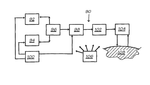
can be generated with an apparatus such as apparatus 90, shown in block
diagram form in
Fig. 6. Apparatus 90 includes a first timing block 92 which generates a
succession of
intervals T1 and T2, and optionally also T5 and T6; a second timing block 94
which generates a
succession of intervals T3 and optionally also T4 and T7; an interconnection
block 96 which
combines the signals from blocks 92 and 94 so that the succession of intervals
Ti and T2
appears only during intervals T3; a voltage or current switch 98 which
generates an output
signal at usable intensity; an optional adjustment block 100 for modifying the
signal timing
and intensity (i.e., amplitude); a filter 102 which removes unwanted signal
components and
preferably also sets transition and decay time constants; a connection block
104 which passes
the signal out to a load 106 (cell culture, tissue, organism or part thereof,
etc.); and a power
supply 108 which provides energy as needed to enable the other components of
apparatus 90
to perform their functions.
When present, adjustment block 100 may provide the capability of selecting
from
among a plurality of alternative, paired values of intervals T1 and T2, of
intervals T4 and T7,
CA 02467713 2015-08-24
16
or of both sets of intervals. More preferably, such paired interval values are
selected so as to
change the operating frequency of apparatus 90 while maintaining a selected
duty cycle, or
vice-versa. For example, one such paired value set of intervals T4 and T7 may
be one in
which both intervals approach zero, thereby making the output a continuous
pulse train such
as waveform 80f.
Optional adjustment block 100 may also provide the capability of selecting
among a
plurality of alternative values of voltage or current levels Li, L2 and Ls in
order to establish an
optimal current density within the living matter being treated (i.e., load
106), as may be
needed or desired for a specific application. To this end, switch 98 may
generate an output
waveform 70 or 80a-80f as a voltage waveform, which is then converted to a
current
waveform by passage through a suitable resistor, resistor network or voltage-
controlled
current source making up a part of filter 102 under the control of adjustment
block 100.
When a charge-balanced output is desired, filter 102 preferably includes one
or more
nonpolarized capacitors, or back-to-back combinations of electrolytic
capacitors, connected in
series with the output so as to block any direct-current component from the
signal unless such
a component is desired for a specific application. However, other types of
devices may also
be useful for filter 102.
Filter 102 preferably also includes suitable devices for blocking frequencies
above a
selected level (i.e., frequencies greater than the highest ones intentionally
generated), to create
a desired transition profile or to prevent interference by external high-
frequency signal
sources, as may be convenient. For example, filter 102 may include a shunt
capacitance
placed across the output lines after the signal has passed through the
previously-mentioned
resistor, resistor network or voltage-controlled current source so as
simultaneously to slow
and control the rate of transitions, to attenuate output frequency components
above about 50
KHz, and to prevent interference with circuit functioning by any radio-
frequency signals
coming from the outside.
Filter 102 may also include any suitable type of rectifier for converting an
otherwise
biphasic output with no net DC content into a quasi-monophasic output with
controlled DC
content (as may be desirable for some wound-healing applications). If
rectification is used, a
switch may also be provided by which rectification may be turned on or off as
may be needed
for a specific case or phase of treatment. With rectification, it may be
convenient to eliminate
interval T.õ or to set output levels L2 and L3 relatively close together.
Blocks 92, 94, 96, 98, 100, 102, 104, 108 of Fig. 6 may be implemented in any
of a
wide variety of ways. For example, timing blocks 92 and 94 may both be astable
multivibrators whose outputs are further processed by digital logic,
constituting
interconnection block 96, in approximately the manner which was described in
U.S. Patent
No. 5,217,009 (which may be referred to for details). Alternatively, timing
block 92 may be an
astable multivibrator with timing block 94 then derived from block 92
digitally, for example,
by a frequency-divider chain. Timing blocks 92 and 94 may both be derived
digitally from a
CA 02467713 2015-08-24
17
common timing source, using a divider chain or microprocessor, in
approximately the manner
which was described in U.S. Patent No. 5,413,596 (which may be referred to for
details). In
yet another approach, both timing blocks 92 and 94 may be astable
multivibrators, with block
94 controlling block 92 so that block 92 runs, generating intervals T1 and T2,
only during
interval T3 and is turned off at other times, in approximately the manner
which was described
in U.S. Patent No. 6,011,994.
A timing block particularly well-suited for generating asymmetric, repeating
waveforms such as 70 and 80a-80f is based on complementary metal-oxide-
semiconductor
(CMOS) logic. It is a little-known fact that a CMOS logic gate can function as
either an
analog or a digital device, or as both at once. This permits many signal
generation and
processing operations to be performed in a surprisingly effective and
straightforward manner
using CMOS logic gates with analog or mixed signals as inputs. A self-
starting, asymmetric
CMOS oscillator 120 (technically, an astable multivibrator) based on this
principle, consisting
of two inverting logic gates 122a and 122b and a handful of passive
components, was
described in U.S. Patent No. 6,011,994 and is shown in schematic form in Fig.
7.
Oscillator 120 generates two complementary outputs 124a and 124b, each
consisting of a
succession of alternating intervals of high and low voltage, whose durations
depend upon the =
values of capacitor 126 and resistors 128a, 128b and 128c, and the polarity of
diode 130.
Such an oscillator can function as either timing block 92 or timing block 94
in Fig. 6. Using
the complementary outputs 124a and 124b in differential mode, rather than
either of the
outputs against a fixed potential, yields a peak-to-peak output voltage of
nearly twice the
supply voltage.
With a diode 130 connected as shown, and = neglecting nonideal behavior of
circuit
components:
T1=1.1 x Ri C,
T2 = (I. 1 x C) / (1/Ri + 1/R2),
F= 1 / (Ti +T2), and
D = T1 /(r, +T2)
where Ti is the "high" output period of waveform 124a, T2 its "low" output
period, R1 the
value of resistor I28a, R2 that of resistor 128b, C that of capacitor 126, F
the oscillation
frequency and D the duty cycle, provided that R3, the value of resistor 128c,
is large
compared with R/ and R2. For waveform 124b, T1 and T2 are reversed. Tj and T2
are also
reversed in both waveforms if the polarity of diode 130 is reversed.
Suitable values for these components may be found by first specifying a
practical
nonpolarized capacitor value typically in the range from about 100 pF to about
1 [LF;
calculating R1 and R2 from the equations
CA 02467713 2004-05-18
WO 03/015866 PCT/US02/26590
18
R1 = Tj /(1.1 x C), and
R2 = 1 / (1.1 X C(1/TI + 1/T2));
assigning R3 any practical value at least twice and preferably approximately
ten times R2; then
optimizing R1 and R2 (by a modest amount of experimentation) to compensate for
the
nonidealities of real-world components. Optimized values for R1 and R2
typically lie within
approximately 20-30% of those calculated as described above. In no case
should R1 or R2
be less than about 3300 Q nor more than about 3.3 MQ, nor R3 greater than
about 22 MQ . If
this occurs, a new value should be chosen for C in order to bring RI, R2 and
R3 back within
these ranges.
An oscillator 120 such as this can provide virtually any desired oscillation
period from
several seconds down to 1 Asec or less, and any desired duty cycle within such
an oscillation.
Particularly useful is the fact that the oscillation frequency can be changed
without
substantially altering the duty cycle, simply by changing the value of
capacitor 126. This
feature makes it possible to select among a plurality of alternative, paired
values of T1 and T2
while preserving a desired duty cycle, for example, through the use of a
switch selecting one
of a plurality of capacitors.
Two such oscillators 120 can be interconnected so that one of them,
oscillating at a
relatively low frequency, controls the second, which oscillates at a much
higher frequency but
only during a selected phase of the lower-frequency oscillation (either T1 or
T2), thereby
generating a waveform similar to that shown in Fig. 1. Such an interconnected
pair of
oscillators 120a, 120b, shown in Fig. 8, can function as timing block 92 and
94 of Fig. 6,
with the connection between the two oscillators serving simultaneously as
interconnection
block 96. An advantage of this approach is that, since the power consumption
of a CMOS
circuit (neglecting output loading) is strongly dependent on the operating
frequency, turning
off the higher-frequency oscillator except during that portion of the lower-
frequency
oscillation when it is needed minimizes the power consumption.
Two such coupled CMOS oscillators can also be used to generate the equalizing
pulse
of interval T4. More preferably, the two complementary outputs of the higher-
frequency
oscillator are buffered and transformed by an added, mixed analog and digital
stage so that
they generate output voltage or current level L1 when in one set of opposite
logic states,
another voltage or current level L2 when in the opposite set, and a third
level L3 when, at the
end of interval T4, both outputs are brought to like logic states.
In a preferred embodiment, apparatus 90 generates a plurality of specific
waveforms
aimed at various biomedical applications, including but not necessarily
limited to fracture
healing, pain relief, and osteoporosis treatment. For example, a particular
embodiment of
apparatus 90 may generate the six waveforms illustrated in Fig. 9, in any of a
plurality of
user-selectable intensities. Here, waveforms 150, 152, and 154 are pulse-burst
type
CA 02467713 2004-05-18
WO 03/015866 PCT/US02/26590
19
waveforms, each having a different set of values for intervals T1, T2, T5 and
T6; while T3, T4
and T7 are the same in all three. Waveforms 156, 158 and 160 are continuous
pulse-train
equivalents of waveforms 150, 152, and 154, respectively, differing from them
chiefly in that
T4 and T7 are in each case are set to zero. An example of a set of timing
intervals for the
waveforms of Fig. 9 is given in Table 1.
Table 1. Timing intervals for waveforms 150, 152, 154, 156, 158, and 160
(Fig. 9).
Timing Interval*
Waveform T1 T2 T3 T4 T5 T6 T7
150 200 30 10 3 50 54
156 200 30 0 50 0
152 600 70 10 3 150 54
158 600 70 0 150 0
154 1500 170 10 3 400 54
160 1500 170 0 400 0
*(T1, T2, T5, and T6 are given in ixsec; T3, T4, and T7 are in msec)
Timing accuracy for the example of Table 1 is about 10% or 20 ptsec,
whichever is larger.
An apparatus 90 with these timing intervals has been cleared by the U.S. Food
and Drug
Administration for use in the relief of chronic pain. Different timing
intervals may also be
useful for some applications.
When one CMOS oscillator of this type controls another in the manner shown,
interval T5 is the starting delay of the higher-frequency oscillator at the
start of a pulse burst
and is typically about one-fourth of interval T1, while interval T6 is simply
that portion of the
last interval T/ which remains at the end of interval T3. Hence, no attempt is
made to define
T6 beyond what has already been given. Intervals T3, T4 and T7 have the same
values for all
three pulse-burst waveforms; for the continuous waveforms, interval T3 is
undefined while T4
and T7 are both zero.
Intervals T/ and T2 are selected so that, for a pulse-burst type waveform,
each burst
may be divided either into approximately 6-8 pulses ("low modulation") as in
waveform
150, approximately 15-32 pulses ("medium modulation") as in waveform 152, or
approximately 35-72 pulses ("high modulation") as in waveform 154. The same
values of
intervals T1 and T2 are used in the corresponding continuous pulse-train
waveforms.
To compensate for variable tissue cross-sections to be treated or differing
optimal
current densities of various tissues, preset intensities for each waveform may
be provided as
shown in Table 2.
CA 02467713 2004-05-18
WO 03/015866 PCT/US02/26590
Table 2. Nominal output current (total output current from connection block
104 into load 106, measured according to ANSI/AAMI Standard No. NS-4-
1985. Within load 106, the current is distributed approximately uniformly
5 across the full cross-section of the load, with local variations
depending on the
particular tissue types present).
Output Current (IAA)
Setting Pulse-Burst Mode Continuous Mode
10 LOW 60 180
MEDIUM 200 600
HIGH 600 1800
In general, pulse-burst operation is recommended for treatment periods of
15 approximately one hour or more; treatment periods up to eight hours per
day or even higher
are recommended for many conditions. Where available treatment time is
restricted to an hour
or less, however, continuous pulse-train operation may be preferred. Low
modulation is
recommended for treating patients with thin or moist skin, medium modulation
for normal
skin, and high modulation for thick or dry skin. Similarly, low intensity is
recommended for
20 use on the fingers, medium intensity on the hands and arms, and high
intensity elsewhere on
the body. However, the optimum combination of settings is best determined
individually for
each particular patient being treated; a modicum of experimentation may be
applied to find the
most effective combination of settings in any particular case. As noted above,
waveforms
150-160 meet all the safety requirements of ANSI/AAMI NS-4-1985. As a result,
an
apparatus 90 with the settings set forth in Tables 1 and 2 can safely be used
wherever a
conventional microcurrent electrostimulator or TENS unit can be used.
An apparatus 90 with the output parameters of Tables 1 and 2 includes parts
corresponding to each of blocks 92-108 of Fig. 6, examples of which will be
set forth
below. While specific, preferred through-hole type parts numbers are sometimes
given in the
following descriptions, it should be understood that different components
(including surface-
mount type devices) and components manufactured according to differing
technologies may
also be useful. Resistors are typically 1/4-watt, metal or metal-oxide film
types with 1%
tolerance unless stated otherwise.
Power supply 108, shown in Fig. 10, includes a replaceable battery 172; a
three-
position, on/off and function selector switch 174; a steering diode 176 for
function selection;
a pair of blocking diodes 178a and 178b to prevent damage should battery 174
be inserted
backwards; and an electrolytic bypass capacitor 180 which provides a charge
reservoir for
circuit operation. No adapter, socket or other device for external power input
is provided. In
a preferred embodiment of the invention, the battery compartment for battery
172 is designed
so that apparatus 90 operates only when the compartment is closed.
CA 02467713 2004-05-18
WO 03/015866 PCT/US02/26590
21
Battery 172 may have a nominal output of nine volts or thereabouts. Output
voltages
in this range may be provided by a series stack of three 3-volt lithium coin
cells with
capacities of at least approximately 270 milliampere-hours each, for example,
Type 2032
lithium coin cells surrounded by a heat-shrunk sleeve trimmed flush with the
most positive
and most negative cell faces. Such a stack powers an apparatus 90 with the
particular
components described below for approximately two weeks of continuous use. For
longer
run times, larger coin cells may be used or a plurality of such cells may be
connected in
parallel. Lithium cells are preferred because of their combination of small
size, long shelf
life, high energy density, and relatively flat discharge curve under low and
approximately
constant loading; however, other types of batteries may also be useful.
In the embodiment shown in Fig. 10, position "A" of selector switch 174
disables
control oscillator 190 via diode 176 and output line 182, selecting continuous
pulse-train
mode; position "B" allows both oscillators to run, generating pulse bursts,
while position "C"
is "off". Positions "C", "B" and "A" of switch 176 thus correspond to "OFF",
"BURST"
and "CONTINUOUS" operating modes, respectively.
Diodes 178a and 178b prevent accidental damage from reversed battery insertion
in
switch positions "A" and "B" respectively. Capacitor 180 provides an energy
buffer to
minimize the effects of rising internal resistance in battery 174 near the end
of the battery's
useful life. Output lines 184 and 186 from capacitor 180 are respectively +9
volts nominal
and ground, supplying power to the remaining circuit blocks including
connections,
otherwise not shown, between these lines and the CMOS logic devices in these
blocks.
Switch 174 may be an on-on-on type, single-pole 3-position (SP3T) miniature
slide
switch, such as an NKK type SS14SDP2. Diodes 176, 178a and 178b are small
general-
purpose silicon rectifiers, such as Diodes Incorporated type BAV19 or a
similar type of
rectifier. Capacitor 180 may be any common, miniature aluminum or tantalum
electrolytic
type with a capacity of at least approximately 100 laF at 10 volts DC or
higher.
Fig. 11 shows timing blocks 92 and 94 in the same configuration previously
shown
in Fig. 8. First timing block 92 includes two CMOS logic gates 190 and 192;
three resistors
194a, 194b and 194c; a capacitor 196; and a diode 198. These components form
an astable,
asymmetric multivibrator as shown in Fig. 6. Gates 190 and 192 may be two of
the four 2-
input NAND gates in a CD4011B quad package, connected with lines 184 and 186
as
positive and negative supply, and preferably with each gate having one input
tied "high" so
that it functions as a simple inverter with minimal input and supply currents.
Alternatively, an
inverter may be formed by tying both gate inputs together.
By way of example, resistors 194a, 194b and 194c may have values of 732 KQ,
212
KQ, and 2.2 MQ, respectively, with tolerances of 1%. Capacitor 196 may be a
polypropylene or polyester film type capacitor with a value of approximately
0.100 uF at
2% tolerance. These components yield a control signal with a relatively low
duty cycle, as
CA 02467713 2004-05-18
WO 03/015866 PCT/US02/26590
22
shown in Fig. 5D, and a frequency of 15 Hz. Other values of resistance and
capacitance may
be used if other duty cycles or frequencies are desired. Exact values may also
differ
depending on factors such as the type of device, manufacturer, and lot number,
but may be
optimized as previously described. Diode 198 is a small general-purpose
silicon rectifier,
preferably a BAV19 or similar type.
Similarly, second timing block 94 consists of two CMOS logic gates 200 and
202;
three resistors 204a, 204b and 204c; three capacitors 206a, 206b and 206c,
only one of
which is selected at a time; and a diode 208. These form the same type of
oscillator just
described, except that this one accepts a control input and generates
complementary outputs in
the manner which was shown in Fig. 7. Gates 200 and 202 are preferably two of
the four 2-
input NAND gates in a CD4011B quad package, connected with lines 184 and 186
as
positive and negative supply.
Gate 200 receives as one input the output of gate 192, so that oscillator 94
is turned
on when this line is "high" and off when it is "low" (this connection
corresponds to
interconnection block 96 of Fig. 6). Thus, when signal 192 has a low duty
cycle, oscillator
94 runs only for a small fraction of the total time, thereby conserving
battery power. Gate
202 has one input tied "high" in the same manner as gates 190 and 192. Gates
200 and 202
respectively feed output lines 210a and 210b with complementary pulse-burst
signals in the
manner which was explained with Fig. 8.
Selection among capacitors 206a, 206b and 206c is made through a three-
position
switch 212, which functions as a part of adjustment block 100 (Fig. 6).
Capacitor 206a has
the highest value of the three, and capacitor 206c the lowest. Hence, these
three capacitors
respectively provide the "LOW", "MEDIUM" and "HIGH" modulation settings.
For purposes of illustration, diode 208 is shown in Fig. 11 with polarity
opposite that
of diode 198. This arrangement causes the generation of complementary outputs
(as shown
in Fig. 7) with a low duty cycle on line 210a and a correspondingly high duty
cycle on line
210b. Alternatively, reversing diode 208 reverses this relationship while the
outputs remain
complementary.
For example, resistors 204a, 204b and 204c may have values of 147 1(Q, 15.4 KR
and 2.2 MQ respectively, with tolerances of 1%. Capacitors 206a, 206b and
206c are
preferably polypropylene or polyester film types with 2% tolerances and
values of .0068
12F, .0027 11F and .001 [IF, respectively. These components yield pulse trains
with high duty
cycles and with approximately frequencies of 600 Hz, 1,600 Hz, and 4,000 Hz,
respectively.
Diode 208 is a small general-purpose silicon rectifier, preferably a BAV19 or
close functional
equivalent.*The optimum values of any circuit components provided herein as
examples may
differ depending on the type of device, manufacturer, lot number, and so
forth, and may be
found by a modest amount of experimentation for each particular application
Voltage switching block 98, filter 102, an associated part of adjustment block
100,
and connection block 104 are shown together in Fig. 12. Voltage switching
block 98
CA 02467713 2004-05-18
WO 03/015866 PCT/US02/26590
23
consists of two pull-up resistors 220a and 220b, two input protection
resistors 222a and
222b, two signal coupling capacitors 224a and 224b, two bypass diodes 226a and
226b, and
two CMOS inverters 228 and 230. For added current-handling capacity, each of
inverters
228 and 230 may be formed by two standard CMOS logic gates of matched
switching
characteristics connected with inputs and outputs in parallel, and powered in
common by lines
184 and 186 as positive and negative supply, rather than by a single gate.
More preferably,
both inverters are formed from the four 2-input NAND gates in a single CD4011B
quad
package or similar devices taken in pairs.
Pull-up resistor 220a and coupling capacitor 224a together form a high-pass
filter
which transfers fast-changing signals from line 210a to the inputs of inverter
228 with
minimal distortion, but draws these inputs to logic "high" when no fast-
changing signals are
present. Resistor 222a and diode 226a prevent voltage or current overshoots
which might
damage the inverter inputs. Resistors 220b and 222b, capacitor 224b and diode
226b serve
an identical function with line 210b and inverter 230. As a result, the
outputs of inverters 228
and 230 reproduce the complementary outputs of gates 202 and 200 respectively
when
oscillator 94 is running, but both assume equal logic "low" potentials if no
transitions have
taken place on these lines within a specified delay time. The differential
voltage between
these outputs then becomes zero, midway between its positive and negative peak
values,
corresponding to interval T7 in Fig. 4.
Filter 102 is made up of capacitors 240a-240d, resistors 244a and 244b, and
capacitor 246. Connected in series with the output of each inverter 228 and
230 is a pair of
electrolytic capacitors 240a and 240b (or 240c and 240d) with their anodes
tied together, thus
forming a single, effectively nonpolarized capacitor which will pass a fast-
changing signal but
block any direct-current component, thereby creating a charge-balanced output.
Nonpolarized
electrolytic capacitors made for audiophile applications may also be useful;
however, these
types of capacitors may have excessive leakage current for use with the
present invention.
Placed in series with each such capacitor pair is a resistor 244a or 244b,
beyond
which both lines are bridged by capacitor 246. The function of resistors 244a
and 244b and
capacitor 246 is to filter out unwanted high-frequency signal components of
signals leaving
the inverters, while simultaneously blocking the entry of outside high-
frequency signals
which might interfere with device functioning. The corner frequency of the
resulting filter is
preferably about 50 KHz. Dividing the resistance equally between resistors
244a and 244b
also enhances safety, since even if any one component should fail, the current
will still be
limited to a safe level.
After the end of a given pulse burst, capacitors 240a-240d discharge, as
indicated by
line 38 of Fig. 1 over interval 36, with a time constant which is set in part
by the component
values in filter 102 and the properties of load 106. When this curve reaches
zero, capacitors
240a-240d hold no net charge.
CA 02467713 2004-05-18
WO 03/015866 PCT/US02/26590
24
At the end of the delay generated by resistors 220a and 222a, capacitor 224a
and
diode 226a, or by their "b" counterparts, the outputs of inverters 228 and 230
assume equal
voltages, both logic "low". If this transition coincides with the passage of
the capacitor
discharge curve through voltage level L2, the discharge curve is truncated at
that point.
Thereafter, since zero voltage is placed across the capacitors and zero charge
remains on
them, the output current is zero until the start of the next pulse burst. Such
truncation is
shown, for example, at the end of interval T4 in waveform 70 of Fig. 13.
While additional components may be needed to find the actual transition after
each
pulse burst, tests of the above-described apparatus 90 under typical loading
conditions
showed that after a 10-millisecond pulse burst, for example, the transition
took place after
about three more milliseconds. Since the curve is not particularly steep at
this point, minor
changes to component values in filter block 102 and to load 106, or to the
electrical
characteristics of the living tissue to which the signal is being delivered,
do not substantially
affect the output. Hence, values for resistor 220a and capacitor 224a (and for
220b and
224b) may be found which give near-optimal performance over substantially all
expected
conditions of use. The resulting delay then becomes T4 (74d in Fig. 4) while
the following,
substantially current-free "rest" period becomes T7 (74g).
Resistors 220a and 222a, capacitor 224a and diode 226a (and their "b"
counterparts)
serve the additional safety function of forcing the outputs of inverters 228
and 230 both to
logic "zero", and thus the output current to zero, in case of oscillator
failure. This feature
prevents electrolytic damage to tissue which might otherwise slowly occur if
the oscillator
failure took place in a device whose capacitors 222a through 222d had higher
than nominal
amounts of DC leakage. Values for resistors 220a and 220b, based on this
criterion, are 681
KQ each; for resistors 222a and 222b, 150 KQ each; and for capacitors 224a and
224b,
0.0068 [IF each. These capacitors are preferably miniature polypropylene or
polyester types
with 2% tolerance. Capacitors 240a-240d are preferably small 10 liF aluminum
or
tantalum electrolytic types rated at 15 volts or higher, although each
directly-connected pair
may optionally be replaced with a single, nonpolarized capacitor of like value
and voltage
rating. Preferred practical values for resistors 244a and 244b are 332 Q each.
Diodes 226a
and 226b are small general-purpose silicon rectifiers, preferably BAV19s or
similar devices.
Fig. 13 illustrates the approximate waveforms 70 and 80 which are produced by
the
above-described circuit under pulsed and continuous operation, respectively.
The voltage
"droop" (that is, decay toward intermediate level L4) is caused by the finite
charge capacity of
the DC-blocking capacitors.
For some applications, such as stimulation of wound healing, it may be
convenient to
superimpose a controlled amount of DC upon waveform 70 rather than to suppress
the DC
content of the output, or to provide the ability to do so as an option.
Preferably, the DC bias
of the waveform is shifted without diminishing its amplitude. Diode 250
provides a simple
rectification device by which this can be done, while switch 252 provides the
flexibility of
CA 02467713 2004-05-18
WO 03/015866 PCT/US02/26590
switching the diode into or out of the circuit to provide either charge-
balanced or DC-biased
operation. Where this flexibility is not desired and only DC-biased operation
is to be used,
the circuit of Fig. 12 may be modified by removing all components between
input 210a and
the junction of resistor 244a and capacitor 246; connecting this junction
directly to positive
5 supply rail 184; and replacing the combination of capacitors 240c and
240d with a short
circuit. This renders levels L2 (76b), L3 (76c) and L4 (76d) substantially
equal while
eliminating voltage droop, as in a waveform 82 (shown in Fig. 14).
The magnitude of the output current delivered to load 106 is determined in
part by
switch 260, which functions as a part of adjustment block 100 by selecting any
one of three
10 different resistors 262a, 262b or 262c to be placed in series with
capacitors 240a and 240b
and resistor 244a. Resistor 262a has the highest value of the three, and
resistor 262c the
lowest. The selected resistor acts in concert with resistors 244a and 244b,
the series
combination of the three plus the internal resistance of inverters 228 and 230
serving to limit
the output current to cell culture, tissue, organism or part thereof 106.
Hence, these three
15 resistors respectively provide the "LOW", "MEDIUM" and "HIGH" output
intensity settings.
Resistors 262a, 262b and 262c may have values of approximately 24.1 KR 3.92
K52, and
332 52, respectively.
Output block 104 consists of diodes 270 and 272, wires 274a and 274b, and
conductive block 276a and 276b by which physical contact is made with the
living tissue
20 (load 106) to be treated. At least one of diodes 270 and 272 is a light-
emitting diode (LED),
such as a Fairchild MV8412, while the other is a small silicon rectifier such
as a BAV19. The
LED may be either diode 270 as shown, or diode 272. However, for DC-biased
(i.e.,
monophasic) operation, the LED is preferably that diode of 270, 272 which
shares the
polarity of diode 250 with respect to the output loop. Alternatively, both
diodes may be
25 LEDs. With the diodes arranged in antiparallel manner as shown (the
anode of each tied to
the cathode of the other) the pair is able to pass a high-frequency signal and
emit light in
proportion to the current flowing. This provides an indication simultaneously
that the battery
is providing adequate operating voltage, that all circuit blocks which it
powers are functioning
correctly, and that wires 274a and 274b and conductive block 276a and 276b are
connected
correctly to load 106.
Wires 274a and 274b are multistranded, fatigue-resistant wires, for example,
22
AWG equivalent wires with 30/37 stranding, insulated with a tough but flexible
nonconductive material such as PVC. Their lengths may be chosen as needed for
a specific
application. Wires 274a and 274b, or sections thereof, may optionally be made
removable
from the remainder of the apparatus as shown, for example, by means of
appropriate, FDA-
acceptable plugs and sockets. Each of the wires may terminate in a 2 mm
(0.080") diameter
metal pin, miniature alligator clip or other device by which easy connection
may be made to
conductive blocks 276a and 276b.
CA 02467713 2004-05-18
WO 03/015866 PCT/US02/26590
26
Conductive blocks 276a and 276b may include electrically-conductive saline
solutions
or gels held in appropriate structures such as disposable or reusable
electrode pads, salt
bridges or other appropriate structures depending upon the intended use and
type of load 106
to be treated. For example, saline gel electrodes may be adhered to the skin
of a human or
animal patient so that the field of current flow which is established between
them includes the
tissues to be treated. An example of such a gel electrode is the Uni-Patch
"Multi-Day" #633;
however, other types of electrodes may also be useful. Alternatively, block
276a and 276b
may be in whole or in part of other materials, such as silver wire or silver-
plated textile fabric,
used in a similar fashion.
Alternatively, an output such as that as shown in Fig. 14 can be generated
more
simply, yet with greater efficiency and more accurate current limiting, using
a circuit 290 as
shown in Fig. 15. Here, signals 210a and 210b (from the circuit of Fig. 11)
are fed, via
resistors 300a and 300b, to the bases of bipolar silicon transistors 302 and
304 respectively.
Each of transistors 302 and 304, together with the associated passive
components, forms a
simple current regulator.
Current passing through a forward-biased semiconductor junction causes a
voltage
drop which is only weakly (i.e., approximately logarithmically) affected by
the amount of
current flowing. For many purposes, this voltage drop, sometimes called a
"diode drop,"
may be assumed to be approximately constant regardless of the current. The
magnitude of the
voltage drop is characteristic of the material: in silicon, for example, it is
typically close to
0.65 volt, while in gallium phosphide (used to make green light-emitting
diodes) it is about
2.1 volt.
Thus, when voltage 210a is low, the current passing through a resistor 300a
and
diodes 306a and 306b sets the base of a PNP transistor 302 two diode drops, or
about 1.3
volt, below positive supply rail 184. The base-emitter junction of transistor
302 cancels one
diode drop of this, while the second diode drop appears between rail 184 and
the emitter, in
this case across a resistor 308 plus a small parasitic resistance (typically
about 10 Q) in the
base-emitter path. The resulting collector current thus equals about 0.65 volt
divided by the
value of a resistor 308 plus 10 Q, unless limited by other components in the
current path.
Transistor 302 therefore sets a maximum limit on the output current.
Similarly, when voltage 210b is high, the current passing through resistor
300b and
diodes 306c and 306d sets the base of an NPN transistor 304 two diode drops
above negative
supply rail 186. Again, the base-emitter junction cancels one diode drop,
while the other
appears between the emitter and rail 186. In this case, a switch 310 allows
any one of a
plurality of resistors 312a, 312b, . . . to be selected. Alternatively, some
combination of one
or more resistors 312a, 312b, . . . might be selected, or a continuously
variable resistance
might be substituted. The resulting collector current is about one diode drop
divided by the
selected resistance plus 10 Q, unless limited by other components.
CA 02467713 2004-05-18
WO 03/015866 PCT/US02/26590
27
Through the combined action of the components shown in Fig. 11 and described
previously, signal line 210a is normally high (near rail 184) but pulses low
(near rail 186)
during each wave train, as indicated by simplified waveform diagram 230a.
Similarly, line
210b is normally low but pulses high with each wave train, as indicated by
diagram 230b.
As a result, both transistors 302 and 304 have their base-emitter junctions
forward-biased
during the pulses of each wave train, allowing collector current to flow, but
not during the
intervals between the pulses or between the wave trains. Current is therefore
provided to the
output only during the pulses of each wave train.
As before, the output is through wires 274a and 274b, electrodes 276a and
276b,
light-emitting diode 270, and load 106 (which may be living tissue), all of
which are placed in
series between the collectors of transistors 302 and 304, so that current
leaving the collector
of transistor 302 passes through them before entering the collector of
transistor 304. The
current passing through load 106 will therefore approximate the smallest of:
(1) 0.65 volt divided by the value of resistor 308 plus 10 Q (transistor 302
dominates);
(2) 0.65 volt divided by the value of the selected resistor 312a, 312b, and so
forth
plus 10 Q (transistor 304 dominates); or
(3) the voltage between rails 184 and 186, minus two silicon and one gallium
phosphide diode drop totaling about 3.4 volts, the result then divided by the
total resistance of
resistor 308, selected resistor 312a, 312b, and so forth, wires 274a and 274b,
electrodes
276a and 276b, material 106, plus 20 Q (load dominates). In this case, the
current may be
arbitrarily small while, with a 9-volt supply, the voltage appearing across
the load will be
approximately 7-8 volts.
Preferably, the lowest-valued of resistors 312a, 312b, . . . is equal to or
slightly
higher than resistor 308, with the others increasing by approximately
logarithmic steps. As a
result, transistor 304 normally dominates unless load 106 is of low
conductivity or there is a
faulty connection in wires 274a and 274b or electrodes 276a and 276b, with the
actual current
being selected by switch 310. For three resistors 312a, 312b and 312c as
shown, whose
values increase in logarithmic steps, the current in load 106 therefore
decreases in proportion
as indicated by simplified waveform diagrams 322a, 322b and 322c respectively.
Should
transistor 304 fail, transistor 302 takes over and maintains current limiting
at a safe, though
no longer user-selectable level. Alternatively, switch 310 and resistors 312a,
312b, . . .
could be connected instead to transistor 302 in place of resistor 308, or
switch 310 might be a
double-pole type with resistors 312a, 312b, . . . duplicated for both
transistors
As described above, light-emitting diode 270 monitors the output current and
signals,
by its flashing, that all connections are secure, the battery is good and
current is being
delivered to load 106. However, since current flows in only one direction
between the output
terminals (out of the collector of transistor 302, through wire 274a, material
106, wire 274b,
CA 02467713 2004-05-18
WO 03/015866 PCT/US02/26590
28
diode 270 and into the collector of transistor 304), no antiparallel diode,
such as diode 272 in
Fig. 12, is needed.
As an example of the circuit of Fig. 15, transistor 302 is a small-signal PNP
type such
as a 2N2907 or MMBT4403LT1, transistor 304 is a small-signal NPN type such as
a
2N2222 or MMBT4401LT1, diodes 306a through 306d are silicon rectifiers such as
BAV19s, resistors 300a and 300b are each 10 1(Q, resistors 308 and 312a are
each 130 Q,
resistor 312b is 412 Q, and resistor 312c is 1400 Q. All resistors have 1%
tolerance.
The resulting maximum current in load 106 is about 4.2 mA with resistor 312a
selected, about 1.4 mA with resistor 312b selected, and about 0.42 mA with
resistor 312c
selected. This current is nearly independent of the electrical characteristics
of load 106,
provided that the load does not dominate as explained above. With a preferred
waveform
timing of 2001,1,sec on and 30 vsec off, repeated for 10 msec 15 times per
second as described
above, the resulting time-averaged DC current delivered to load 106 is
approximately 600
vamp with switch 310 selecting resistor 312a, 200 vamp with the switch
selecting resistor
312b, or 60 vamp with the switch selecting resistor 312c.
For some applications, such as the stimulation of nerve regeneration, it may
be useful
not only to superimpose a DC component upon the AC waveform, but also to
reverse the
polarity of this DC component at regular intervals, typically each ten to
sixty minutes. A
waveform including such reversal is shown in Figs. 16A and 16B.
Fig. 16A shows a waveform 330 for a short interval including two pulse trains
340a
and 340b as previously described, a polarity reversal 342, followed by two
additional pulse
trains 340c and 340d. Voltage levels 76a and 76b are set about equidistant
from zero but
have opposite polarities, while levels 76c and 76d are both set close to zero.
For clarity,
reversal 342 is shown as occurring during an interval between pulse trains,
but it could as
easily take place at any other point in the waveform or at different such
points at different
times. Note that on reversal, the voltage level during the pulses and the
level during the
intervals between them switch places so that the time-averaged DC component is
also
reversed in polarity while remaining roughly constant in amplitude.
Fig. 16B shows waveform 330 for a longer period, including three reversals
342a,
342b and 342c, illustrating how the voltage level during the pulses and the
level in the
intervals between them repeatedly switch places. For purposes of illustration,
only five pulse
trains are shown during each period between reversals. In a real application,
however, the
number of pulse trains between reversals would more likely be several
thousands or tens of
thousands.
For some applications, as in treatment during sleep in conditions for which a
treatment
period of less than eight hours has been found optimal, it may be useful to
turn off the
treatment unit after a selected length of time. Fig. 17 illustrates a waveform
332 similar to
CA 02467713 2004-05-18
WO 03/015866 PCT/US02/26590
29
that in Fig. 16B, but also including an automatic shutoff 344, following which
the output
voltage and current fall to and remain at zero.
Fig. 18 illustrates a circuit 348 capable of generating waveforms such as
those shown
in Figs. 14, 16A, 16B, and 17. As in Fig. 11, a control oscillator 92
generates the pulse-
burst envelope and a pulse oscillator 94 then generates the bursts themselves.
All components of control oscillator 92 are as previously described, except
that logic
gate 192 is provided with a second control input line 350 to turn the control
oscillator, and
thereby the pulse oscillator also, off upon automatic shutdown so as to
minimize power
consumption and prolong battery life. For example, gate 192 may be a NOR gate
as shown,
so that a negative signal on a line 350 permits normal operation but a
positive signal there
turns it off. Alternatively, gate 192 may be a NAND gate, turned off by the
application of a
negative signal to line 350. Other control methods are also possible.
Similarly, all components of pulse oscillator 94 are as previously described,
except
that only one of the two possible, complementary outputs is taken, for
example, through
signal line 210b. Rather than feed the output filter directly, this signal is
applied to one input
of an exclusive-OR (XOR) gate 352. Such a gate has the property that if a
steady or changing
logic-level signal is fed to one of its inputs and a steady low level to the
second input, the
logic signal appears, faithfully reproduced, at its output. If the second
input is held high
instead, the signal applied to the first input appears inverted at the output.
Signal polarity
reversal, as illustrated in Figs. 16A, 16B and 17, may thus be accomplished
simply by
changing a signal 354 applied to the first input from logic high to logic low,
or vice-versa.
A first output signal 356a from gate 352 is then passed through an inverter
358,
creating a second output signal 356b which is complementary to first signal
356a, thus
undergoing polarity reversal at the same time but in the opposite direction.
First and second signals 356a and 356b then pass to components which drive the
output to zero after automatic turnoff. For DC-biased operation these may
simply be a pair of
logic gates 360a and 360b, of the same kind as gate 192 and fed by the same
control signal
350. Such gates produce outputs 362a and 362b which are complementaiy in one
state of
signal 350 but equal, yielding a zero output, in the other. For example, using
NOR gates as
shown, outputs 362a and 362b are complementary so long as signal 350 remains
at logic
low, but both drop to zero, yielding zero output, when signal 350 changes to
logic high.
Signals 362a and 362b may then be connected to additional filtering and output
components, for example taking the form which was shown in Fig. 18 with the
deletions
suggested in the text for DC-biased operation.
For charge-balanced operation with automatic turnoff, gates 362, 358, 360a and
360b
may be eliminated, control line 350 and gate 192 retained as shown in Fig. 18,
and signals
210a and 210b taken from the pulse oscillator as shown in Fig. 11 and filtered
as shown in
Fig. 12. The simple shutdown of the control oscillator by signal 350, causing
in turn a
CA 02467713 2004-05-18
WO 03/015866
PCT/US02/26590
shutdown of the pulse oscillator through the action of the components shown in
Fig. 12,
suffices to drive the output to zero and hold it there without any other
circuit modifications.
Shutdown signal 350, polarity-reversing signal 354, or both, may be derived
from the
control oscillator output 370 by a conventional digital divider 372, such as a
multistage binary
5 divider chain.
For example, dividing the preferred control-oscillator frequency of 15 Hz by
2" to
create signal 354 yields polarity reversal at intervals of about 9.1 minutes,
while division by
215 yields reversal at 18.2-minute intervals. Either of these will likely
suffice for many
applications with no need for more elaborate divider circuitry. Alternatively,
any convenient
10 divider circuitry may be employed with the invention.
Similarly, dividing the preferred control-oscillator frequency by 217 yields a
shutoff
signal 350 becoming active after approximately 1 hour and 13 minutes, by 218
after 2 hours
and 26 minutes, by 219 after 4 hours and 51 minutes, and by 220 after 9 hours
and 43
minutes. Again, these intervals will likely suffice for many applications,
although different
15 divider circuitry (including circuitry that provides different
intervals) may be used if desired.
An advantage of deriving the shutdown timing from the control oscillator is
that, once
shutdown has occurred, the control oscillator is disabled and no further
counting takes place.
Thus, once shut down, the device remains that way with no need for further
attention until it
is manually reset. This may be done either by turning the stimulator off and
then on again, or
20 (again, if desired) by pressing a "reset" button sending an appropriate
signal 374 to a reset
input of divider chain 372.
Alternatively, another oscillator of the same or a different type, such as a
crystal
oscillator of the type used in digital watches, might be used to create
shutdown signal 350,
polarity-reversing signal 354, or both.
25 An apparatus 90, made using the component values given above and
including all or
any selected subset of the functions described above, may be mounted in a
small, lightweight
housing of molded plastic or other suitable material, preferably a housing
with a pocket clip
or other means for convenient mounting to a bandage, cast, wrist or other
band, or article of
clothing. Most preferably, the housing is no larger than necessary to hold the
described
30 devices and the circuit board or boards which bear them. Suitable
housings need be no larger
than approximately 5 cm x 6 cm x 2 cm (about 2.0" x 2.5" x 0.75") or
thereabouts. Smaller
housings may be useful if some or all of the described functions of apparatus
90 are
implemented using surface-mount components, rather than the through-hole ones
which have
in some cases been identified in the descriptions above.
Apparatus 90 is lightweight, compact, self-contained, cost-effective to
manufacture
and maintain, and convenient to carry or wear for extended periods. It is safe
for
unsupervised home use without the need for special training, and able to
generate the signals
just described and deliver them efficiently through conductive pads making
direct contact with
the skin. Since only low voltages and currents are used, apparatus 90 does not
pose a shock
CA 02467713 2015-08-24
31
hazard even in case of malfunction. Power is furnished by compact and
inexpensive
batteries, needing replacement only once in several weeks of use.
An apparatus according to the invention is used to provide electrotherapeutic
treatment
for human and animal patients, including but not limited to healing
acceleration, relief of acute
or chronic pain, and relief of swelling and/or inflammation. However, the
apparatus need not
be confined to use with intact organisms, since isolated cells or tissue
cultures can also be
affected by electrotherapeutic waveforms (appropriate electrical stimuli have
been observed to
modify the rates of cell metabolism, secretion, and replication). Isolated
skin cells, for
example, might be treated with selected waveforms in an appropriate medium to
increase cell
proliferation and differentiation in the preparation of tissue-cultured,
autogenous skin-graft
material. As another example, the growth of bacteria genetically engineered to
produce a
desirable product, such as human insulin, might be accelerated, or their
secretion of the
desired product increased, by treatment with a suitable waveform.
With respect to the above description of the invention, it is to be realized
that the
optimum dimensional relationships for the parts of the invention, to include
variations in size,
materials, shape, form, function and manner of operation, assembly and use,
are deemed
readily apparent and obvious to one skilled in the art, and all equivalent
relationships to those
illustrated in the drawings and described in the specification are intended to
be encompassed
by the present invention.
Therefore, the foregoing description is considered as illustrative only of the
principles
of the invention. Further, since numerous modifications and changes will
readily occur to
those skilled in the art, it is not desired to limit the invention to the
exact construction and
operation shown and described, and accordingly, all suitable modifications and
equivalents
may be resorted to, falling within the scope of the invention. Thus, it will
be apparent to
those skilled in the art that many changes and substitutions can be made to
the preferred
embodiment herein described without departing from the scope of the present
invention as defined by the appended claims.