Note: Descriptions are shown in the official language in which they were submitted.
CA 02467806 2009-11-17
71495-63
-1-
METHOD FOR POLISHING A SUBSTRATE SURFACE
Field of the Invention
The present invention relates generally to the preparation of semiconductor
substrate
surfaces, and more specifically to preparing substrate surfaces using chemical
mechanical
polishing (CMP).
Background of the Invention
Chemical mechanical polishing (CMP) is a process that is used to polish
surfaces of
semiconductor wafers. In particular, CMP employs both physical and chemical
forces to
polish wafer surfaces. First, a load force is applied to the back of a wafer
while it rests on a
polishing pad. Both the pad and the wafer are then counter-rotated while
slurry containing
both abrasives and reactive chemicals is passed underneath.
CMP is typically used to planarize a surface of a wafer for the purpose of
creating an
is integrated circuit. CMP has emerged as the planarization method of choice
because of its
ability to planarize over longer lengths than traditional planarization
techniques. As
discussed, CMP is a combination of a chemical reaction and mechanical action.
First, the
slurry weakens the wafer surface and the slurry particles, in addition to
particles located on
the pad, complete material removal from the wafer surface.
It is desired to use aluminum nitride (AIN) as a substrate material for
creating
commercial semiconductor devices, however, there are problems in processing
AIN surfaces
to derive substrate surfaces suitable for epitaxial growth. For example,
current CMP
processes damage the AIN material making it unsuitable for epitaxial growth.
It would be
CA 02467806 2004-05-19
WO 03/043780 PCT/US02/37135
-2-
beneficial to have an improved method for polishing AIN wafers that produces a
quality
surface suitable for epitaxial growth.
Summary of the Invention
One illustrative embodiment of the invention is directed to a method of
preparing a
surface of a substrate, the method comprising the acts of preparing the
surface of the substrate
for a chemical mechanical polishing (CMP) process, performing the CMP process
on the
surface of the substrate, and finishing the surface of the substrate, wherein
the act of
performing the CMP process further comprises an act of applying an abrasive
suspension in a
solution during the CMP process. According to one aspect of the invention, a
method is
provided wherein the substrate is aluminum nitride (A1N).
According to another aspect of the invention, the abrasive suspension in the
solution
further comprises a silica suspension in a hydroxide (basic) solution.
According to another
aspect of the invention, the abrasive suspension includes a KOH-based slurry.
According to
one aspect of the invention, the abrasive suspension in the solution further
comprises a silica
particles suspended in an ammonia-based slurry.
According to another aspect of the invention, the act of performing the CMP
process
includes an act of applying the abrasive suspension at a rate of approximately
0.5 mL per
minute for a circular 8.0" diameter polishing surface. According to one aspect
of the
invention, the act of performing the CMP process includes an act of
maintaining a polishing
speed of the sample in a range of approximately 13 to 18 m/sec.
According to another aspect of the invention, the act of preparing includes
cleaning a
polishing apparatus prior to polishing the surface of the substrate to
substantially reduce
contamination of the polishing surface. According to one aspect of the
invention, the act of
finishing the surface of the substrate includes an act of substantially
rinsing the abrasive
suspension from the surface of the substrate. According to another aspect of
the invention,
the method further comrpises cleaning, during the preparing acts, the surface
of the substrate
with a solvent. According to another aspect of the invention, the substrate is
an on-axis, Al-
polarity, c-face surface, and the abrasive suspension has a pH value of
approximately 10.5 or
greater. According to another aspect of the invention, an substrate is
provided produced by
CA 02467806 2004-05-19
WO 03/043780 PCT/US02/37135
-3-
the method. According to another aspect of the invention, a device having a
substrate
produced by the method is provided.
According to another aspect of the invention, a method is provided for
preparing a
surface of a substrate. The method comprises acts of preparing the surface of
the substrate for
a chemical mechanical polishing (CMP) process, the act of preparing comprising
acts of
determining an orientation of the substrate; and performing a removal of the
surface of the
substrate based on the orientation. According to another aspect of the
invention, the substrate
is A1N, and the act of determining an orientation includes an act of
determining, for the A1N
substrate, at least one face of the A1N substrate and its orientation to the
surface to be
polished. According to another aspect, the act of performing a removal
includes an act of
determining a period of removal based on the orientation. '
According to another aspect of the invention, the act of performing a removal
includes
an act of removing exposed off-axis material from the substrate surface.
According to another
aspect, the act of removing the exposed off-axis material includes removing
between 50 and
100 m of material from the substrate surface.
According to another aspect, the substrate includes a surface normal to be
polished,
and the act of determining an orientation includes determining, for a given
face of the
substrate, an orientation of the normal surface with respect to the given
face. According to
another aspect of the invention, the act of performing a removal of the
surface of the substrate
based on the orientation of the normal surface with respect to the given face.
According to another aspect, the substrate includes an Al-polarity side of c-
face
substrate, and the act of performing a removal includes performing at least
one of a dry
grinding and polishing using a polymer diamond suspension to prepare the Al-
polarity side of
the c-face substrate. According to another aspect of the invention, the A1N
substrate includes
a non-polar surface, and the act or performing a removal further comprises an
act of removing
between 10 and 20 gm of the non-polar surface.
According to another aspect of the invention, the method further comprises an
act of
performing the chemical mechanical polishing (CMP) process, and a polishing of
the
substrate surface is performed based on the orientation. According to another
aspect,
CA 02467806 2009-11-17
71495-63
-4-
the polishing further comprises an act of polishing the substrate surface with
a
slurry having a pH value, and the slurry being selected based on the face of
the
substrate and the pH value.
According to another aspect, the substrate is AIN, and the substrate
surface is the on-axis Al-polarity, c-face surface, and the pH value of the
selected
slurry is greater than 10.5.
According to another aspect of the invention, a substrate is provided
produced by the method. According to another aspect of the invention, a device
having a substrate produced by the method is provided.
According to one aspect of the present invention, there is provided a
method of preparing a surface of a single-crystal aluminum nitride (AIN)
substrate,
the method comprising: preparing the surface of the single-crystal AIN
substrate
for a chemical mechanical polishing (CMP) process; performing the CMP process
on the surface of the single-crystal AIN substrate; and finishing the surface
of the
single-crystal AIN substrate, wherein performing the CMP process comprises
applying an abrasive suspension in a solution consisting substantially of a
hydroxide during the CMP process.
According to other aspects of the present invention, there are
provided a substrate prepared by a method described herein and a device having
a substrate prepared by a method described herein.
Further features and advantages of the present invention as well as
the structure and operation of various embodiments of the present invention
are
described in detail below with reference to the accompanying drawings. In the
drawings, like reference numerals indicate like or functionally similar
elements.
Additionally, the left-most one or two digits of a reference numeral
identifies the
drawing in which the reference numeral first appears.
CA 02467806 2009-11-17
71495-63
-4a-
Brief Description of the Drawings
The invention is pointed out with particularity in the appended claims. The
above and
further advantages of this invention may be better understood by referring to
the following
description when taken in conjunction with the accompanying drawings in which
similar
reference numbers indicate the same or similar elements.
s
In the drawings,
Figure 1 shows a conventional CMP apparatus that may be used to polish
substrate
surfaces in a CMP process according to one embodiment of the invention;
Figure 2 shows a flow chart of a process used to polish a substrate surface
according
to one embodiment of the invention;
Figure 3 shows a more detailed process for polishing a substrate surface
according to =
one embodiment of the invention;
Figure 4 shows an AFM image of an Al-polarity c-face of an AIN substrate after
performing CMP polishing according to one embodiment of the invention; and
CA 02467806 2004-05-19
Printed: 15-01-2004 DESCPAMD L US0237135
-5-
Figure 5 shows an AFM image of an AIN substrate surface tilted 45 degrees with
respect to a c-axis direction of the AIN substrate, the surface pictured after
performing CMP
polishing according to one embodiment of the invention.
Detailed Description
The use of single crystal III-nitrides allow improved epitaxial growth,
improved
thermal and chemical compatibility, as well as improved thermal conductivity.
Applications of
to wide-bandgap and high-temperature semiconductors including the development
of blue/UV
solid-state charge injection lasers, UV optical sources and detectors, high
power microwave
devices, high power switches, and high temperature applications. However,
there is a need to
obtain a method for suitably preparing surfaces of aluminum nitrides (AIN)
substrates for
epitaxial growth to produce these devices. For example, nitrides (e.g. AIN,
Al., Ga(t-.)N, etc.)
]5 may be epitaxially grown on single crystal AIN substrates by, for example,
Organometallic
Vapor Phase Epitaxy (OMVPE) and other formation processes.
Device fabrication on AIN substrates generally involves the epitaxial growth
of a
device layer. The quality of this device layer depends on the quality of the
surface of the AIN
substrate. Despite the best polishing techniques, the wafer surface can retain
polishing defects
20 such as micro-damage and surface roughness. Surface defects are known to
effect the quality
of finished semiconductors prepared through epitaxial growth. It is believed
that conventional
polishing procedures damage the AIN surface both at a submicron scale and just
under the AIN
surface in such a way that the substrate is unsuitable for epitaxial growth.
Difficulty arises in
preparing such surfaces because the AIN surface is unable to be polished using
conventional
25 CMP process without introducing surface defects. Because conventional CMP
techniques
damage the AIN surface, a method that produces an atomically smooth surface
suitable for
epitaxial growth for AIN crystals is desired.
According to one aspect of the invention, an improved process for preparing a
surface
of a substrate is provided wherein the surface of the substrate is prepared
for a chemical
3o mechanical polishing (CMP) process, the CMP process is performed on the
surface of the
1 ! AMENDED SHEET 122-12-2003
CA 02467806 2004-05-19
WO 03/043780 PCT/US02/37135
-6-
substrate, and the surface of the substrate is finished to clear the substrate
surface of any
active ingredients from the CMP process. Also, an improved substrate produced
by the
method is provided. According to one aspect of the invention, particular
polishing materials
and procedures may be used that allow for increased quality of A1N substrate
surfaces.
To employ A1N crystals as substrates for epitaxial growth of other compound
semiconductors such as GaN, InN, or 2H-SiC, large area, high perfection A1N
wafers are
needed. After growing AIN boules, the boules are generally cut into wafers
using annular
diamond saws or wire saws and then the surface of each is ground and polished
flat.
According to one embodiment of the invention, A1N crystal surfaces (e.g., the
a, +c or -c
surfaces of A1N) are polished using CMP to derive surfaces suitable for
epitaxial growth.
Optimally, these polished surfaces are flat, highly perfect surfaces with a
minimum of
scratches, pits, or damage dislocations and other subsurface damage. Also,
these polished
surfaces are also free of aluminum oxide coating or islands.
In any grinding process, the powder employed for grinding should have a
microhardness greater than or equal to that of the crystal being ground. The
basic goal is to
remove material from the crystal in a short period of time. The polishing is
intended to give a
mirror-like finish to the surface, and leave a damage-free crystal underneath.
This polishing
process is much like "chemical-mechanical-planarization" processes as are
known in the art
which are used most frequently to planarize wafer surfaces of multilayer
devices. In this
process, the polishing lubricant actually reacts slowly with the crystal being
polished. The
slurry and abrasive pad are designed to continuously remove the reaction
products without
appreciably damaging the underlying crystal.
In CMP, high elevation features of a wafer are selectively removed (i.e.,
material from
high elevation features is removed more rapidly than material at lower
elevations), resulting
in a surface having an improved planarity. Mechanical polishing, assisted by
chemical action,
produces such selective material removal. The process is performed by mounting
the wafer
face down on a carrier. The carrier is then pressed against the rotating
platen containing a
polishing pad. The carrier itself is also rotated. An abrasive-containing
aqueous slurry is
dripped onto the table, saturating the pad. Conventionally, the slurry
comprises abrasives of
CA 02467806 2004-05-19
Printed: 15-01-2004' DESCPAMD US0237135
-7-
silica, alumina, ceria, or other nanometer-size particles suspended in an
alkaline or acidic
medium.
According to one aspect of the invention, it is realized that orientation
affects
mechanical preparation of a substrate surface prior to CMP processing. So-
called c-face
substrates are produced when the AIN crystal is sliced perpendicular to the c-
axis of the
crystal. These c-face substrates are polar and the surfaces on the two sides
of the substrate will
have quite different properties. One side of the substrate is aluminum (AI)
terminated (or so-
called Al-polarity, c-face) and the other side is nitrogen (N) terminated (or
so-called N-
polarity, c-face).
When the AIN crystal is cut so that the c-axis of the crystal is contained in
the plane of
the substrate, a non-polar substrate is produced wherein the two surfaces have
identical
behavior. Substrates that are cut at some angle away from the c-axis (other
than 90 ) also
demonstrate some polarity effects, but these effects are not as strong as the
effects of c-face
substrates. C-face substrates are currently being used to produce electronic
devices that take
advantage of polar effects to create a high-density electron gas without any
or with minimal
doping. However, optoelectronic devices are expected to be better if non-polar
substrates are
used.
According to one embodiment of the invention, it is realized that substantial
differences
exist for optimal preparation of the substrates surfaces with different
crystallographic
orientations. In the case of an AIN substrate, it is realized that the Al-
terminated, c-face is not
reactive with water, but the N-terminated c-face is reactive with water, along
with non-polar
faces. During wet lapping and polishing, the Al-polarity face tends to chip
under the same
conditions that are well-suited to mechanically polish the non AI-polarity
faces and for Al-
polarity faces where the c-axis is oriented 20 degrees or more away from the
surface normal of
the substrate. (Effectively, wet mechanical processing used on orientations
other than the on-
axis c-face is actually a chemical mechanical processing with a fixed
abrasive). According to
one embodiment of the invention, dry grinding and polymer diamond suspensions
are used to
prepare the Al-polarity side of c-face substrates that are close to on-axis
(misorientation less
than approximately 20 ). Even under strictly
1
~2 AMENDED SHEET 22-12-2003
CA 02467806 2004-05-19
WO 03/043780 PCT/US02/37135
-8-
mechanical polishing, the removal rates observed for the on-axis, Al-polarity
surface is lower
than for all other crystal orientations.
According to one embodiment of the invention, it is realized that the amount
of
material that should be removed during the mechanical processing prior to fine
mechanical
polishing and CMP depends upon quality of the saw cut. Typically between 50
and 100 m
must be removed to level the irregular cut of the saw for an annular saw. At
this point, the
sample is generally planar and should have a low pit density, and the sample
may be subjected
to fine mechanical processing. In this step, it is realized, according to one
embodiment, that
planarity of the samples be brought to the highest level for c-face, Al-
polarity substrate
surfaces, because it is realized that any exposed off-axis material will lead
to undercutting of
the desired surface during CMP. For non-polar surfaces, the high chemical
reactivity allows
planarization during CMP (few microscopically viewable pits and scratches are
allowable and
does not cause the CMP undercutting effects on the Al-polarity surfaces. Fine
mechanical
processing generally involves a measured removal totally between 10 and 20 m
of sample
thickness.
According to one embodiment of the invention, it is realized that the removal
rate
during CMP is very much a function of the crystallographic orientation of the
substrate
surface. For the Al-polarity, c-face substrates, the removal rate increases
from around 1 pm
per hour to over 10 m per hour as the angle between the surface normal and the
c-axis is
increased from near zero to over 20 . For the non-polar and N-polarity, c-face
surfaces, the
removal rate is mechanically limited by the abrasive particles in the slurry.
Example
Figure 1 shows a conventional CMP apparatus that may be used to polish
substrate
surfaces in a CMP process according to one embodiment of the invention. A
wafer 101 to be
polished is mounted on a wafer carrier 102 which generally includes a backing
film 109
positioned between wafer 101 and a chuck 108 which holds the wafer and the
wafer carrier
102. Wafer carrier 102 is rotated by a spindle 105. A force is applied to the
wafer carrier 102
to contact the wafer 101 with one or more polishing pads 103A-103B. The one or
more
polishing pads 103A-103B are adhered to a platen 106 which also rotates.
Further, a slurry
CA 02467806 2009-11-17
71495-63
-9-
107 is applied to the pad 103A-103B and the drip rate is controlled, for
example, by a control
flow dispenser (not shown).
It should be appreciated that other CMP tools and/or polishing apparatus may
be used
and the invention is not limited to any particular CMP tools or polishing
configurations.
According to one aspect of the invention, the CMP process may involve
polishing the
substrate using a slurry, the slurry comprising an abrasive suspension in a
solution such that
the slurry is capable of etching the substrate surface and creating a finished
surface suitable
for epitaxial growth. For example, a silica suspension in a solution may be
used. This
solution may be, for example, a hydroxide (basic) solution. Such a slurry is
available
TM
1 0 commercially, for example, as the KOH-based CMP slurry known in the art as
SS-25 (Semi-
Sperse 25), available from Cabot Microelectronics or the Syton slurry
available from
Monsanto.
According to one embodiment of the invention, it is realized that a higher pH
KOH
TM _
slurry works better for the Al-polarity, c-face surface. The SS25 slurry has a
pH of 11Ø Its
high pH distinguishes it from other commercially availably KOH slurries (like
Syton and
Glanzox) which have lower pH. For the on-axis Al-polarity, c-face surface, it
is realized,
according to one embodiment of the invention, that the pH should be over 10.5
to obtain
observable removal rates.
It should be appreciated that other slurry types may be used. For example,
diamond,
silicon carbide, or other material may be used in a slurry. Also, other
commercially-available
TM TM
slurries are available (e.g., SS-25-E and SS-225 (ammonia hydroxid-based) both
of which are
TM TM
available from Cabot Microelectronics, AM 100 and Rodel 2371 (ammonia-based
slurries)).
Such chemical/mechanical polishing methods are particularly suitable for
preparing
very hard surfaces, such as aluminum nitride (A1N) surfaces. It should be
appreciated that
.25 various aspects of the invention reduce an amount of impurities and
surface defects
introduced into the AIN crystal substrate by the polishing procedure.
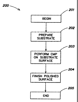
Figure 2 shows a process 200 for polishing a substrate according to one
embodiment
of the invention. At block 201, process 200 begins. At block 202, the
substrate is prepared
for polishing. This may include removal of contamination from the surface of
the substrate,
the polishing apparatus and environment. Such contamination is generally
responsible for the
CA 02467806 2004-05-19
WO 03/043780 PCT/US02/37135
-10-
introduction of surface defects during the polishing process. At block 203, a
CMP process is
performed on the substrate surface. In the case of A1N, the CMP process may
include
polishing the surface using a slurry having a hydroxide solution. For example,
the SS-25
slurry available from Cabot Microelectronics may be used. It should be
appreciated that the
invention is not limited to the type of slurry, and that other appropriate
slurries may be used as
discussed above. At block 204, the polished sample is finished. This may
involve, for
example, removal of the sample from the polishing apparatus and carefully
cleaning the
sample to remove any reactive agents introduced by the polishing process. At
block 205,
process 200 ends.
Figure 3 shows a more detailed process 300 for polishing a substrate according
to one
embodiment of the invention. At block 301, process 300 begins.
According to one embodiment of the invention, the A1N substrate is prepared
for a
CMP process. More particularly, the environment and wafer are cleaned of
possible
contaminants, and the polishing apparatus adjusted to apply the correct
polishing force to the
wafer. The following example is a procedure for preparing the substrate
according to one
embodiment of the invention:
1. Preparation of Substrate and Apparatus for CMP Process
1. The sample surface and mounting block should be cleaned of substantially
all possible
contamination particles (e.g., wax, dirty, and larger mechanical grit
particles). This is
typically done with, for example, organic solvent (e.g., by acetone and/or
methanol) cleaning
performed at block 302. Also, any remaining particles from previous
processings (e.g., CMP
fluid residue) should be cleaned from all surfaces that contact the polishing
area so as to
reduce the likelihood of contaminating the polishing surface and potentially
damaging the
substrate surface.
2. The mounting block is then prepared to hold the sample at block 303. For
example,
the sample may be adhered to a surface of the mounting block. The mounting
block is then
switched from the "mechanical" process fixture to the "CMP" process fixture.
According to
one embodiment of the invention, these fixtures may be identical items; their
use may be
CA 02467806 2004-05-19
WO 03/043780 PCT/US02/37135
-11-
segregated to avoid cross contamination between the mechanical and chemical
mechanical
polishing.
3. The mounted sample may have the vertical offset corrected to allow the
sample
appropriate contact with the polishing surface. A mass to ensure proper down
force can be
added to the block at 304. Pressure in a range of 5 x 10⁵ to 7 x 10⁵ N/m2 have
been shown to
be suitable. These are conditions that have yielded the most consistent
results for both non-
polar and polar faces. However, it should be appreciated that the invention is
not limited to
any particular set of conditions.
According to one embodiment of the invention, a CMP process may be performed
on
the prepared substrate surface. In one aspect of the invention, SS-25 (Semi-
Sperse 25) slurry
available from the Cabot Microelectronics Corporation may be used to polish an
A1N
substrate.
II. CMP Process
The following is a detailed sequence of steps, according to one embodiment of
the
invention, to prepare an A1N substrate surface and the drip rates for a CMP
process according
to one embodiment of the invention.
= A new "Multitex 1000" fine polishing pad or any other suitable fine
polishing pad should
be applied to the polishing table (platen). Generally, such a polishing pad
has a self-
adhesive backing to adhere it to the platen surface. At block 305, the
polishing pad is
adhered to the platen surface. For best results, the polishing pad should be
applied to the
polishing deck in such a way to ensure that the pad is not placed with space
behind the
pad causing it to be uneven. For example, the polishing pad may be rolled onto
the table
from the lead edge to the other side with a cleaned rod so that spaces behind
the pad can
be avoided.
CA 02467806 2004-05-19
WO 03/043780 PCT/US02/37135
-12-
= At block 306, the pad surface may be cleaned. For example, the pad may be
cleaned with
distilled water, saturated with water and the empty pad and platen surface
rotated (e.g.,
45-60 RPM or 13 to 18 m/sec in the sample path) on the pad for 10 to 15
minutes. During
this cleaning process, the sample (with the substrate to be polished) should
be lifted out of
contact with the polishing surface. During this time, the surface of the pad
should be
thoroughly rinsed with filtered distilled water. This is performed to ensure
that both the
pad and the fixture have been completely cleaned of all dust and cross-
contaminated
particles.
= At block 307, the slurry drip rate and rotation of the fixture should be set
for polishing.
During this rotation cleaning of the surface, the drip rate should be set
using an
appropriate flow control dispenser. The rate that has yielded the best and
most consistent
polishing results has been 3 drops of SS-25 slurry and distilled water per
minute
(approximately 0.5 mL/minute of each of the CMP fluid and distilled water for
a circular
8.0" diameter polishing surface). It should be appreciated, however, that the
invention is
not limited to any particular drip rate, and that drip rate depends on the
type of slurry used,
pressure applied to the sample, and rotation speed. With this average drip
rate set, the SS-
slurry should be allowed to drip onto the polishing surface allowing the
lapping fixture
to evenly spread the solution and fill the sample area with a consistent level
of abrasive
20 particles and reactive solution prior to polishing the substrate surface.
The polishing pad
may be preconditioned in this manner prior to polishing for approximately 30-
60 minutes
or any other appropriate time to allow for substantially even distribution of
slurry and
etchant over the surface of the pad.
25 = Following the proper rate confirmation and with the observation of proper
rotation of the
fixture, then the sample may be lowered on the surface to begin the CMP
process. At
block, 308, the sample is polished.
Although a typical process time (polishing time) for this step is
approximately 1 hour,
a process time in a range of 5 minutes to 100 hours has been shown to
adequately polish a
CA 02467806 2004-05-19
WO 03/043780 PCT/US02/37135
-13-
surface. It should be understood that the invention is not limited to a
particular process time,
but rather, the process time range is provided by way of example.
Although the material removal depends highly upon the crystal quality and the
orientation of the sample, common values range from 0.1 m (Al face c-axis) to
60 m (N
face c-axis) for 1 hour processing.
According to one embodiment of the invention, the sample is cleaned to remove
any
contamination from the CMP process, and to remove traces of reacting chemicals
from the
substrate surface to stop any residual reactions with the substrate.
III. Finishing
1. At block 309, the sample is rinsed. At the end of the CMP process, the
sample should be
lifted from the polishing surface and immediately rinsed, for example, with
distilled water.
This is performed to ensure that the reaction between the A1N and any of the
active
ingredients in the slurry be stopped, and to remove abrasives that may dry to
the prepared
surface.
2. Following this rinsing, the sample is carefully cleaned at block 310 with
suitable organic
solvents to remove the agent bonding the substrate to the substrate holder.
Mounting
waxes soluble in these solvents and other common sample holding techniques may
be
used to hold the substrates, as well as other adhesive film and vacuum
chucking
techniques. Each of these holding techniques may need different substrate
debonding
procedures at block 311, as is well-known in the art.
3. Following the CMP processing, the sample surface should be cleaned very
well at block
312. For example, the sample surface may be cleaned prior to removal of the
sample from
the mounting block, and then the entire sample may be cleaned when removed.
4. At block 311, process 300 ends.
CA 02467806 2004-05-19
WO 03/043780 PCT/US02/37135
-14-
Figure 4 shows an AFM image of the Al-polarity of the c-face substrate after
polishing
according to one embodiment of the invention. The substrate surface is
oriented with its
normal approximately 5 off the direction of the c-axis. It can be seen that
the surface is
nearly atomically flat. Analysis of a wider area shows that all mechanical
damage has been
removed. Similarly smooth surfaces may be obtained for the N-polarity of a c-
face substrate.
Figure 5 shows an AFM image of a substrate after polishing according to one
embodiment of the invention. The surface is tilted 45 with respect to the c-
axis direction. As
can be observed, the substrate surface is nearly atomically flat. Evidence of
mechanical
damage has been removed. The crossed box on the center was eliminated from the
image for
to the statistical analysis.
Having described several embodiments of the invention in detail, various
modifications and improvements will readily occur to those skilled in the art.
Such
modifications and improvements are intended to be within the spirit and scope
of the
invention. Accordingly, the foregoing description is by way of example only,
and is not
intended as limiting. The invention is limited only as defined by the
following claims and the
equivalents thereto.
What is claimed is: