Note: Descriptions are shown in the official language in which they were submitted.
CA 02468079 2007-06-08
-1-
PCT/US02/37816
CORRECTIVE PHASE QUADRATURE MODULATOR SYSTEM AND
METHOD
BACKGROUND OF THE INVENTION
The present invention relates to a system and method for producing a
quadrature
QAM signal as a function of the difference in the phase relationship between
the two
components signals of the phase-corrected QAM signal and the phase
relationship
between the two input signals, typically referred to as the "I" and "Q"
sil,mals.
One use for the QAM modulator is in a wireless communication system,
although the present inventive system and method is not omitted to wireless
communication systems. A conventional QAM modulator typically receives an in-
phase signal ("I signal"), a quadrature signal ("Q signal"), each of which
contains
digital data to be communicated to a receiver, and a first carrier signal. The
I and Q
signals are typically phase shifted 900 each form the other. A first carrier
signal is
tpyically used to produce a second carrier signal by means of a phase shifting
circuit
which shifts the phase of the first carrier signal by 90 . The I signal is
used to
modulate the first carrier signal to thereby produce a first component signals
and the
Q signal is used to modulate the second carrier signal to thereby produce a
second
component signal. The first and second component signals are conventionally
added
together to produce an output QAM signal which is then transmitted, either
over a
wireless or wired system, to a receiver.
The output of the QAM modulator is characteristically a constellation of
signal points when viewed in the I-Q plane. The minimum distance ("dmin")
between
any two points of the signal constellation can be seen as a measure of the
susceptibility of the communication system to degradation caused by noise.
Noise
typically causes the data being received by the receiver to be misinterpreted
thereby
increasing the bit error rate of the system and resulting in the
retransmission of the
bits received in error. The higher the bit error rate, the more
retransmissions required
and the less data throughput realized by the cominunication system. One way to
CA 02468079 2007-06-08
-2-
PCT/US02/37816
increase the data throughput is to increase the order of modulation. However,
as the
order of modulation increases, the more points populate the signal
constellation
resulting in a smaller dmiõ of the signal constellation and consequently
increasing the
susceptibility of the communication system to noise.
Ideally, the phase shift between the first and second carrier signals in the
modulator is 90 which will result in the maximum dmiõ for a given modulation
order
and associated signal constellation. In practical systems, however, there is
always
some phase imbalance, i.e., a phase relationship between the two carrier
signals of
other than 90 , which results in a smaller dmin for the signal constellation.
7'ypical prior art systems attempt to solve the phase imbalance problem a
variety of ways. One prior art system and method is to characterize the phase
imbalance for a particular communication system and to then statically
multiply one
of the two carrier signals by a constant amount to compensate for the
characterized
phase imbalance. The problem with this approach is that the phase imbalance
may
vary depending on non-constant factors, such as ambient temperature.
Additionally,
these prior art systems are only effective when the phase imbalance is
relatively small.
Another prior art system and method may attempt to adjust the level of one or
both of
the input signals to a QAM modulator as a function of some measured parameter,
such as ambient temperature, in an open-loop feedback system. Such open loop
control systems may provide some limited degree oI'control and these systems
typically increase the complexity and cost of a QAM modulator by requiring a
CPU,
memory and attendant circuitry. 'I'he degree of control attainable is only as
good as
the program in the CPU.
Yet another prior art system may employ digital techniques to correct the
phase imbalance by sing intermediate frequency ("IF") based components. These
systems suffer from the added complexity and expense of the added IF
components
such as CPU's, up-converters, multiple filter stages, etc. Yet another typical
prior art
systems and methods may additionally attempt to compensate for phase imbalance
due to a change in ambient temperature by compensating one or both of the
carrier
signals by a predetermined amount. 'l'hese systems require the added
complexity and
CA 02468079 2007-06-08
-3-
PCT/UM2/37816
cost of temperature measuring equipment along with the attendant signal
processing
hardware and software.
SUMIVIARY OF THE INVENTION
One embodiment of the present invention avoids the problems and limitations
of the prior art by providing a feedback loop to dynamically control the
amount of
phase shift applied to the carrier signal as a function of the difference in
the phase
relationship of the two component signals comprising the output QAM signal and
the
phase relationship of the I and Q input signals. The inventive system provides
dynamic, closed loop control based on the current operating conditions while
adding
only a few simple, inexpensive components.
Accordingly, it is an object of the present invention to obviate many of the
above problenis and limitations in the prior art and to provide a novel system
and
method for generating a phase corrected QAM output signal.
It is another object of the present invention to provide a novel system and
method for controlling the amount of phase shift applied to the carrier signal
as a
funclion of the difference between the phase relationship of the two component
signals compromising the output QAM signal and the phase relationship between
the
input I and Q signals.
It is yet another object of the present invention to provide a novel system
and
method of producing an error signal as a function of the relative phase
imbalances
between the input and output signals in a QAM modulator where the error signal
is
used to phase correct one of the two carrier signals for the QAM modulator.
It is still another object of the present invention to provide a novel system
and
method for a phase correcting M-QAM modulator operating in the RF frequency
range.
It is a further object of the present invention to provide a novel system and
method for
producing a phase corrected QAM signal representative of an I and a Q input
signal
where the I sigmal modulates a I"irst carrier signal and the Q sil,mal
modulates a second
carrier signal produced by applying the first carrier signal to one or more
phase
shifting circuits.
CA 02468079 2004-05-21
WO 03/047090 PCT/US02/37816
It is yet a further object of the present invention to provide a novel M-QAM
modulator comprising a feedback loop for dynamically adjusting the phase
relationship between the two carrier signals as a function of the difference
between
the phase relationship of the two carrier signals and the phase relationship
of the I and
Q input signals.
It is still a further object of the present invention to provide a novel
system and
method for producing a QAM signal in a phase correcting QAM modulator where
one
of the carrier signals is derived by applying the other carrier signal to at
least one
phase shifting circuit where the amount of phase shift applied is a function
of the
difference in phase between a first signal representative of the phase
relationship of
the two component signals comprising the QAM output signal and a second signal
representative of the phase relationship of the two input signals to the QAM
modulator.
It is an additional object of the present invention to provide a novel system
and
method for providing closed-loop feedback control for dynamically controlling
the
amount of phase shift applied to a first carrier signal for producing a second
carrier
signal where the amount of phase shift applied is a function of the difference
between
the phase relationship of the two coinponent signals comprising an output QAM
signal and the phase relationship between the two input (I and Q) signals.
These and many other objects and advantages of the present invention will be
readily apparent to one skilled in the art to which the invention pertains
from a perusal
of the claims, the appended drawings, and the following detailed description
of the
preferred embodiments.
BRIEF DESCRIPTION OF THE DRAWINGS
Figure 1 is a conventional prior art quadrature modulator without phase
correction.
Figure 2 is a notional graph of a 16 QAM constellation with a 90 phase shift
between the I and Q components, depicting a minimum distance between adjacent
constellation points.
-4-
CA 02468079 2004-05-21
WO 03/047090 PCT/US02/37816
Figure 3 is a notional graph of a 16 QAM constellation with less than 900
phase shift between the I and Q components, depicting a smaller minimum
distance
between adjacent constellation points.
Figure 4 is a functional block diagram of a prior art quadrature modulator
illustrating one method of phase correction.
Figure 5 is a functional block diagram of a prior art quadrature modulator
illustrating another method of phase correction.
Figure 6 is a functional block diagram of an embodiment of a quadrature
modulator according to the present invention illustrating a feedback loop to
control
the amount of phase shift applied to the carrier signal in the phase shifter.
Figure 7 is a functional bloclc diagrain of another embodiment of a quadrature
modulator according to the present invention illustrating a plurality of
cascaded phase
shifters for applying a phase shift to the carrier signal where the phase
shifters are
controlled by the feedback loop.
Figure 8 is a functional block diagram of yet another embodiment of a
quadrature modulator according to the present invention illustrating two
cascaded
phase shifters, one for applying a fixed amount of phase shift to the carrier
signal and
the other for applying a phase shift to the carrier signal the amount of which
is
controlled by the feedback loop.
Figure 9 is a functional block diagram of still another embodiment of a
quadrature modulator according to the present invention illustrating a
feedbaclc loop
to control the amount of level adjustment applied to the I signal.
Figure 10 is a functional block diagram of still yet another embodiment of a
quadrature modulator according to the present invention illustrating feedback
loops to
control the amount of level adjustment applied to the I and Q signals.
DESCRIPTION OF PREFERRED EMBODIMENTS
With reference to the drawings, like numerals represent lilce components
throughout the several drawings.
-5-
CA 02468079 2007-06-08
-6-
PCT/US02/37816
As discussed above and shown in Figure 1, a conventional QAM modulator
100 receives an in-phase signal, or the I signal 110, conventionally expressed
as
1=1(t)
And a quadrature signal, or the Q signal 120 conventionally expressed as
Q=q(t)
where i(t) and q(t) may represent information to be transmitted from a
transmitter to a
receiver in a communication system.
The I and Q signals typically contain digitized data to be transmitted to a
receiver over a carrier wave. A first carrier signal 130, which is
conventionally
generated by an oscillator 101, is applied to a multiplier 103 to be modulated
by the I
signal 110 to produce the first component signal 150. Any standard means known
in
Lhe art to generate a carrier signal is contemplated by the presenL invention.
The first
carrier signal 130 is also applied to a phase shifting circuit 102 which
ideally shifts
the phase of the first carrier signal by 90 to thereby produce a second
carrier signal
140. The second carrier signal is applied to the multiplier 104 to be
modulated by the
Q signal 120 to produce the second component signal 160. The first and second
component signals are combined in the adder 105 to thereby produce the QAM
output
signal 170.
The QAM output signal, when viewed on the I-Q plane, may be visualized as
a signal constellation of points. Figure 2 is a notional graph of an ideal 16
QAM
orthogonal signal constellation 200 in the I-Q plane with a 90 phase shift
between the
I and Q components. Although a 16 QAM signal constellation is shown, it is to
be
understood that the present invention is not limited to 16 QAM but rather the
present
inventive system and method is operational at any order of modulation, i.e.,
any M-
ary signal constellation. As is evidence from the conventional expressions of
the I
and Q signals above, the I axis is the horizontal axis and the Q axis is the
vertical axis.
The signal constellation points are arranged in a well-defined pattern and the
minimum distance 21, dmiõl, between any two points in the signal constellation
can be
defined. I Figure 2, dmiõi is defined as the distance between signal
constellation points
22 and 23.
CA 02468079 2007-06-08
-7-
PCTILIS02/37816
A phase imbalance of a between the I and Q signals, i.e., the I and Q signals
are offset from each other by (90 + a) in pllase, results in the I and ! axes
being offset
by a , as shown notionally in Figure 3. Along with the offset in the I and Q@
axes is
a distortion of the signal constellation 300, shown partially in Figure 3 for
clarity.
The minimum distance 31, dmin2, between any two points in the signal
constellation
can be defined. In figure 3, dmin2, is defined as the distance between signal
constellation points 32 and 33. due to the distortion in the signal
constellation caused
by the phase imbalance of u , dminz < dminl =
With attention now to Figure 4, a functional block diagram depicting a prior
art phase-compensating QAM modulator 400 is depicted where similar numerals
depict similar components and signals with the respective components and
signals of
the QAM modulator 100 depicted in Figure 1. The basic operation of the phase
compensating QAM modulator 400 depicted in Figure 4 is similar to the
operation of
the QAM modulator 100 depicted in Figure 1 except as noted below. The prior
art
phase-compensating modulator 400 includes a level adjuster 406 which
multiplies the
Q signa1420 by a constant predeterniined amount. The constant predetermined
amount of adjustment is designed to compensate for a know phase imbalance for
a
given set of operating conditions. The output of the level adjuster 406 is
combined
with the I signal in adder 407. The output of the adder 407 is applied to the
multiplier
403 in a similar manner as the I signal 110 is applied to the multiplier 103
in Figure 1.
The remaining operation of the phase-compensating QAM modulator 400 in Figure
4
is similar to the operation of the QAM modulator 100 in Figure 1. As discussed
above, the limitation of the prior art phase-compensating QAM modulator 4090
is that
he modulator can only compensate for known, constant phase imbalances and
cannot
react effectively to time-varying imbalances. Therefore, dynamic compensation
of
the phase imbalance cannot be achieved based on actual operating conditions.
With attention now to Figure 5, a functional block diagram depicting a prior
art phase-compensating QAN1 modulator 500 is depicted where similar numerals
depict similar components and signals with the respective components and
signals of
the QAM modulator 100 depicted in Figure 1. The basic operation of the phase
CA 02468079 2004-05-21
WO 03/047090 PCT/US02/37816
compensating QAM modulator 500 depicted in Figure 5 is similar to the
operation of
the QAM modulator 100 depicted in Figure 1 except as noted below. The I signal
510
and the Q signal 520 are each applied to the level adjusters 508 and 509. The
level
adjusters may be controlled by control signal 580 and 590, respectively. The
output
of the level adjuster 508 is applied to the multiplier 503 for modulating the
first
carrier signal 530 to produce the first component signal 550. Likewise, the
output of
the level adjuster 509 is applied to the multiplier 504 for modulating the
second
carrier signal 540 to produce the second component signal 560. The control
signals
580 and 590 may be generated from a lookup table or a CPU so as to supply
either a
constant predetermined level adjustment to the I and Q signals or as a
function of an
external measurement, such as ambient temperature, in an open-loop control
mode.
The remaining operation of the phase-compensating QAM modulator 500 in Figure
5
is similar to the operation of the QAM modulator 100 in Figure 1.
Turning attention now to the inventive system and method, one embodiment
of the present invention is depicted in the functional block diagram in Figure
6 wliere
similar numerals depict similar components and signals with the respective
components and signals of the QAM modulator 100 depicted in Figure 1. The
basic
operation of the phase compensating QAM modulator 600 depicted in Figure 6 is
similar to the operation of the QAM modulator 100 depicted in Figure 1 except
as
noted below.
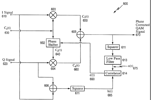
The first carrier signal 630, cl(t), is applied to the phase shifter circuit
602,
which produces the second carrier signal 640, c2(t), by adjusting the phase of
the first
carrier signal by an amount controlled by the error signal 690, e(t). The I
signal 610
modulates the first carrier signal 630 in multiplier 603 to produce the first
component
signal 650, c3(t). Likewise, the Q signal 620 modulates the second carrier
signa1640
in multiplier 604 to produce the second component signa1660, c4(t). The first
and
second component signals 650 and 660, respectively, are combined in adder 605
to
produce the phase-corrected QAM signal 670.
The error signal 690 is representative of the difference between the phase
relationship of the first and second component signals 650 and 660,
respectively, and
-8-
CA 02468079 2007-06-08
-9-
PCT/iJS02/37816
the phase relationship of the I and Q signals 610 and 620 respectively. The
phase
relationship of the first and second coinponent signals rnay be determined by
passing
the phase-corrected QAM signa1670 through a squarer circuit 611, the output of
which is passed through a low pass filter 613 to strip off the carrier signals
and the
associated harmonics. The resulting signal a(t), 675, is representative of the
phase
relationship of the first and second cornponent signals 650 and 660,
respectively. The
I and Q signals are combined in the adder 606, the output of which is applied
to
another squarer circuit 611. The output sil,mal 685 of this squarer circuit,
b(t), is
representative o the phase relationship of the I and Q signals 610 and 620,
respectively. 1'he signals a(t) and b(t) are both applied to the correlator
614 which
determines the correlation between signals a(t) and b(t). The correlator
produces an
error signal 690, e(t) that is proportional to the correlation between signals
a(t) and
b(t), which in turn is proportional to the phase imbalance between the first
and second
component signals 650 and 660, respectively. The error signal 690, e(t), is
fed back
to the phase shifter 602 to dynamically correct the phase of the second
carrier signal
c2(t) and therefore correct the phase of the second component signal c4(t) to
ensure
that the first and second component signals 650 and 660, respectively,
maintain a 90
phase orientation from each other based on the actual current phase
relationship of the
first and second component signals.
The squarer circuit 611 may comprise a schottky diode in a multiplier circuit,
although the present invention is not limited to any particular implementation
of the
squarer circuit.
With reference directed towards Figure 7, a second embodiment of the present
inventive system and method is depicted in a functional block diagram where
similar
numerals depict similar components and signals with the respective components
and
signals of the phase-compensating QAM modulator 600 depicted in Figure 6. The
basic operation of the phase-compensating QAM modulator 700 depicted in Figure
7
is similar to the operation oCthe phase compensating QAM modulator 600
depicted in
Figure 6 except as noted below.
CA 02468079 2004-05-21
WO 03/047090 PCT/US02/37816
As can be seen by a comparison of Figures 6 and 7, the phase-compensating
QAM modulator 700 differs from the phase-compensating modulator 600 by
replacing the phase shifter 602 with a cascaded series of phase shifters 702-
1, 702-2,
through 702-N. Since each individual phase shifter may operate over a limited
range
and therefore only be able to compensate for a small variation of phase
imbalance, the
cascaded approach shown in Figure 7 will be able to compensate for a larger
phase
imbalance.
With reference directed towards Figure 8, a third einbodiment of the present
inventive system and method id depicted in a functional block diagram where
similar
numerals depict similar components and signals with the respective components
and
signals of the phase-coinpensating QAM modulator 600 depicted in Figure 6. The
basic operation of the phase-compensating QAM modulator 800 depicted in Figure
8
is similar to the operation of the phase compensating QAM modulator 600
depicted in
Figure 6 except as noted below.
As can be seen by a coinparison of Figures 6 and 8, the phase-compensating
QAM modulator 800 differs from the phase-compensating QAM modulator 600 by
replacing the phase shifter 602 with a cascaded series of two phase shifters
802-1 and
802-2. The phase shifter 802-1 applies a fixed amount of phase shift to the
first
carrier signal 830. The amount of phase shift applied by the phase shifter 802-
1 is
less than 90 . The phase shifter 802-2 applies an amount of phase shift
controlled by
the error signal 890, e(t), which is a function of the difference between the
phase
relationship of the first and second component signals 850 and 860,
respectively (c3(t)
and c4(t), respectively) and the phase relationship of the I and q signals,
810 and 820,
respectively, as described above for the operation of the phase-compensating
QAM
modulator in Figure 6. The combination of the amount of constant phase shift
added
to the first carrier signal 630, cl(t), by the phase shifter 802-1 and the
amount of
variable phase shift added to the first carrier signal by the phase shifter
802-2
maintains the phase relationship between the first and second component
signals, 850
and 860, respectively, at 90 .
-10-
CA 02468079 2004-05-21
WO 03/047090 PCT/US02/37816
Other preferred embodiments of the present inventive system and method are
shown in Figure 9 and Figure 10 where like numerals represent like components
with
Figure 4 and Figure 5, respectively and similar numerals represent similar
signals
with Figure 6. Figure 9 is a modification of the prior art system shown in
Figure 4. A
feedback loop 900 is added to the device in Figure 4 to dynamically adjust the
amount
of level adjustment applied to the input Q signa1920. As can be seen in Figure
9, the
feedbaclc loop 900 supplies the error signal 990, e(t), to the level adjuster
406 to
thereby dynamically adjust for phase imbalance. As noted above in the
discussion of
Figure 4, the device depicted in Figure 4 includes the level adjuster 406
which
multiplies the Q signa1420 by a constant predetermined amount and adds the
resultant
signal to the I signal 410 to compensate for a known phase imbalance. The
device in
Figure 4 is not capable of dynamically adjusting the amount by which the Q
signal
420 is modified. The inventive device depicted in F'igure 9 dynamically
adjusts the
amount by which the Q signa1920 is modified as a function of the actual phase
inibalance detected by the feedback loop 900.
Similarly, Figure 10 is a modification of the prior art systein shown in
Figure
5. A feedback loop 1000 is added to the device in Figure 5 to dynamically
adjust the
amount of level adjustment applied to the input I and Q signals. As can be
seen in
Figure 10, the feedbaclc loop 1000 supplies the error signal 1090, e(t), to
the level
adjusters 508 and 509 to thereby dynamically adjust for phase imbalance. As
noted
above in the discussion of Figure 5, the device depicted in Figure 5 includes
the level
adjusters 508 and 509 which each multiply the I and Q signals, 510 and 520,
respectively, by a constant predetermined amount to compensate for a lcnown
phase
imbalance. The device in Figure 5 is capable of open loop control by measuring
an
external condition, such as anibient temperature, and sending control signals
580 and
590 to the level adjusters 508 and 509, respectively, to dynamically adjust
the amount
by which the I and Q signals are modified. However, the device in Figure 5 is
incapable of closed-loop dynamic control of the level adjusters 508 and 509
based on
a direct measurement of the phase imbalance. The inventive device depicted in
Figure 10 dynamically adjusts the amount by which the I and Q signals, 1010
and
-11-
CA 02468079 2004-05-21
WO 03/047090 PCT/US02/37816
1020, respectively, are modified in a closed-loop feedback mode by the
feedbaclc loop
1000 as a function of the actual phase imbalance detected.
While preferred embodiments of the present invention have been described, it
is to be understood that the embodiments described are illustrative only and
that the
scope of the invention is to be defined solely by the appended claims when
accorded a
full range of equivalence, many variations and modifications naturally
occurring to
those of skill in the art from a perusal hereof.
-12-