Note: Descriptions are shown in the official language in which they were submitted.
CA 02468251 2004-05-25
WO 03/046536 PCT/EP02/13309
1 THE USE OF 1D SEMICONDUCTOR MATERIALS AS CHEMICAL SENSING
MATERIALS, PRODUCED AND OPERATED CLOSE TO ROOM TEMPERATURE
Description
The invention relates to a chemical sensor device, a method for obtaining such
chemical
sensor device and a method for detecting an analyte by using said chemical
sensor
device.
In recent years much effort has been made to develop devices, which mimic the
sense of
smell or taste. Such devices, which are usually called electronic noses and
electronic
tongues, respectively, would be well suited for a broad variety of
applications, such as
entertainment robots, identification systems, quality control systems,
environmental
monitoring, and medical diagnostics. However, up to now only a limited number
of
electronic nose devices have been marketed. Although these devices are capable
of
identifyixig or classifying some "odour" samples, further improvements are
necessary to
fulfil the needs for many advanced applications mentioned above. These
applications
often require higher sensitivity, higher discrimination capability, faster
response, better
stability, and lower power consumption. Since such features strongly depend on
the
characteristics of the chemical sensors used in the device, there is a strong
demand for
improved sensors meeting the requirements for advanced e-nose and e-tongue
applications. An overview of sensor principles currently under development is
given in
J.W. Gardner and P.N. Bartlett, Electronic noses - Principles and
applications, 1999,
pages 67 - 116 Oxford University Press, Oxford.
There are several gas sensors available on the market, among which are metal
oxide
sensors, often referred to as Tagushi sensors. They are composed of metal
oxides)
having a porous form, generally doped with a metal. They are operated at
elevated
temperatures of 100 to 600 °C in order to allow combustion of the
analyte at the metal
oxide surface, inducing a change of oxygen concentration and therefore a
change in
conductance. Metal oxide sensors are generally employed as single device to
detect toxic
or flammable gases. They can also be employed as arrays for electronic noses,
but their
use for odour recognition was up-to-now limited by the lack of selectivity.
J. Kong, N.R. Franklin, C. Zhou, M.G. Chapline, S. Peng, K. Cho and K. Dai,
Science,
2000, 287, 622 - 625 describe chemical sensors based on individual single-
walled
carbon nanotubes (SWNTs). Upon exposure to gaseous molecules such as N02 or
NH3,
the electrical resistance of a semiconducting SWNT is found to change by up to
three
orders of magnitude within several seconds of exposure to analyte molecules at
room
temperature. The chemical sensors are obtained by controlled chemical vapour
SUBSTITUTE SHEET (RULE 26)
CA 02468251 2004-05-25
WO 03/046536 PCT/EP02/13309
2
deposition growth of individual SWNTs from patterned catalyst islands on
Si02/Si
substrates. Sensor reversibility is achieved by slow recovery under ambient
conditions
or by heating to high temperatures. After e.g. the NOa-flow is replaced by
pure Ar, the
conductance of the SWNT sample slowly recovers with a typical recovery time of
about
12 hours at room temperature.
Z. W. Pan, Z.R. Dai and Z.L. Wang, Science, 2001, 291, 1947 - 1949, describe
the
synthesis of ultralong beltlike nanostructures, so-called nanobelts, of
semiconducting
oxides of zinc, tin, indium, cadmium, and gallium by evaporating the desired
commercial metal oxide at high temperatures. The as-synthesized oxide
nanobelts are
pure, structurally uniform, and single crystalline, and most of them are free
from
defects and dislocations. They have rectangle cross section with typical width
of 30 to
300 nanometers, width-to-thickness ratios of 5 to 10, and lengths of up to a
few
millimetres. A possible use of doped nanobelts as nanosize sensor is
suggested.
V. Bondarenka, S. Grebinskij, S. Mickevicius, H. Tsardauskas, Z. Martunas, V.
Volkov
and G. Zakharova, Phys. Stat. Sol., 1998, A 169, 289 - 294, have investigated
the
influence of humidity on the electrical properties of poly-vanadium acid
xerogels and
xerogels based on poly-vanadium acid where vanadium is partly substituted by
molybdenum or titanium. The conductance of thin-film samples increases with an
increase in humidity as an exponential function and therefore those films are
suitable
for the fabrication of humidity sensors. Thin films of the vanadium-metal-
oxygen
materials were produced by the sol-gel technology. The vanadium pentoxide
powder and
the other components were dissolved in hydrogen peroxide at 273 K. Then the
solution
was heated in an open beaker at 353 K for one/two hours. The obtained gels
were
deposited by a screen-printing method on substrates and baked at 333 K in air.
All
compounds such obtained have a layered structure with interlayer distances of
11,1 to
11,5 A. The amount of water contained in the compounds depends on the relative
humidity RH and increases with an increase in RH.
S. Capone, R. Rella, P. Siciliano and L. Vasanelli, Thin Solid Films, 1999,
350, 264 -
268, investigated the physical and gas sensing properties of bulk material
V205 and
W03 thin films. Gas-sensitive films of vanadium oxide and tungsten oxide were
prepared by means of sputtering technique in a thickness of about 200 nm.
Samples for
gas testing were placed onto a heated sample holder and exposed to different
gas
concentrations. For both materials at high temperatures a strong exponential
dependence of the electrical conductivity on the temperature was observed.
Upon
CA 02468251 2004-05-25
WO 03/046536 PCT/EP02/13309
3
exposure to NO gas an increase of the electrical resistance of the films was
observed.
WO3-based sensors exhibited higher sensitivity values than V~05 ones. In
addition,
tungsten oxide thin filins were also able to detect very low concentrations of
NO in the
sub-ppm range. V~05 could be used for detection of high concentration of NO,
up to a
range of 50 - 500 ppm.
Z.A. Ansari, R.N. Kareka and R.C. Aiyer, Thin Solid Films, 1997, 305, 330 -
335
describe a humidity sensor using planar optical waveguides with claddings of
various
oxide materials, among others bulk-Va05. The planar waveguides were fabricated
on a
soda-lime glass substrate using an ion-exchange process. Films of porous
semiconducting oxides were screen printed on the waveguide surface. The
relative
humidity (RH) was varied from 3 to 98 %. At a cladding length of 3 mm and a
cladding
thickness of 25 ,um V205 exhibited a response time of 5 s and a recovery time
of 30 min.
A hysteresis of 8 % is observed for V205 cladding.
R. Rella, P. Siciliano, A. Cricenti, R. Generosi, L. Vanzetti, M. Anderle and
C. Coluzza,
Thin Solid Films, 1999, 349, 254 - 259, studied the physical properties and
gas-surface
interaction of bulk vanadium oxide thin films. Thin films of vanadium oxide
were
prepared by means of r.f. reactive sputtering. For evaluation of sensing
properties the
films were electrically tested in presence of different gases. Films grown
with 15
oxygen in an Ar-O~-mixture exhibited best sensing properties, giving a maximum
response at a working temperature ranging between 280 and 300 °C.
In most cases vanadium pentoxide is only a secondary component in the
sensitive
coating employed in combination with a more sensitive material, e.g. W03. X.
Wang, N.
Miura and N. Yamazone, Sensors and Actuators, 2000, B66, 74 - 76, report on
W03-
based sensing materials for NH3 and NO detection. Gas sensing materials loaded
with 1
wt.-% metal oxides were prepared. The sensing properties of these materials
towards
NH3 and NO were better than of sensing films of pure W03.
The use of vanadium pentoxide films as temperature sensor is described by Z.
S. El
Mandouh and M.S. Selim, Thin Solid Films, 2000, 371, 259 - 263. The vanadium
pentoxide films were prepared by an inorganic sol-gel method. The temperature
coefficient of resistance, (3T, is 2 % K-1, which indicates, that V~05 can be
used as a
thermoresistor.
CA 02468251 2004-05-25
WO 03/046536 PCT/EP02/13309
4
W098/26871 discloses nanotubes made from transitions metal oxides, preferably
from
a vanadium oxide of variable valence. The nanotubes show oxidation-reduction
activities and are particularly suited as an active material for catalytic
reactions. In the
experimental part synthesis of vanadium oxide nanotubes and the structure of
the
nanotubes obtained is described.
WO01 /44796 discloses a nanotube device comprising at least one nanotube,
preferably
a carbon nanotube, which is electrically connected with its ends to first and
second
conducting elements. The nanotube device may be used as a chemical or
biological
sensor. To tune the sensitivity of the device to a variety of molecular
species the
nanotubes may be modified by coating, or decorating with one or more sensing
agents,
so as to impart sensitivity to a particular species in its environment. The
nanotubes
may also be formed from other materials than carbon, e.g. silicon. Detection
of various
analytes is demonstrated in the experiments. Experiments were done on NOZ and
NH3
gas, thioles, HZ, CO and avidin (a protein). Modification of the sensitivity
by depositing
metal particles, e.g. gold, platinum of nickel, metal oxides, e.g. TiO~, or
biological
species on the sensing agent is also described.
Several types of sensors can be employed at room temperature and show good
selectivity to organics. The most commonly encountered are conducting polymer
chemiresistors, polymer based SAW (Surface Acoustic Wave) and BAW (Bulk
Acoustic
Wave) devices. However, some of these sensors suffer from low sensitivity like
for
example conducting polymer chemiresistors to gases. Devices based on
mechanical
transducers like cantilever and BAW devices are harder to incorporate into
integrated
circuits than the ones based on electrical transducers. For optical detection
based
sensors, the complexity of the transducer may be a limiting factor, especially
when
miniaturisation is considered. Concerning electrochemical cells, they are of
limited use
in the gas sensor domain but are gaining importance for electronic tongues.
A general problem in the use of sensors is humidity. Found in a large majority
of
samples it decreases the detection capabilities. The first reason is related
to the fact
that water will influence the analyte partitioning in the sensor medium or
weaken the
interactions of the analyte with the sensor medium. An example is the
detection of an
aroma of wine. One has to be capable of detecting traces of an aromatic
compound
among a matrix containing large amounts of water and alcohol. A second problem
is
that a change in humidity can be seen as a false detection. For example in the
case of
CA 02468251 2004-05-25
WO 03/046536 PCT/EP02/13309
CO detection, a 20 % change in relative humidity should not be interpreted as
a 50 ppm
CO.
A way to minimize the humidity problem is to dry the analyte. One can
dehydrate the
5 sample itself before analysis, for example dehydrating cheese before sensory
analysis.
The drawback is that the smell may denature during the process because
volatiles are
removed or decomposed. The headspace of the sample can also be dried before
reaching
the detector. This can for example be performed using a nafion filter. Water
will be
filtered off but some components of the analyte, like alcohols, will also be
removed,
partially or completely. Water can also be eliminated by separating the
different
chemicals of a sample using techniques like gas chromatography or similar
techniques.
Only a limited number of reports exist where humidity is of advantage, meaning
the
sensors show an increase of sensitivity with increasing humidity. Kappler, J.;
Tomescu,
A.; Barsan, N.; Weimar, U.; Thin Solid Films 2001, 391, 186 - 191, report on
an
increase of sensitivity of Sn02 gas sensors operated at elevated temperature
toward CO
with increasing humidity. The sensor's response (R°,r/Rco) increased
from 5 to 30 by
increasing the humidity from 0 to 50 % relative humidity. Sadaoka, Y.; Sakai,
Y.;
Murata, Y.U.; Sensors and Actuators 1993, B 13-14, 420 - 423 report a similar
behavior
of an optical sensor based on calcein-poly(acrylonitrile) in the case of
ammonia
detection. The sensitivity increased when I/Io (optical intensity ratio)
decreased from
0.95 to 0.83 under dry air and 50 % relative humidity, respectively. Another
illustration
is based on host molecules (tecton DM 189) deposited on a mass-sensitive
device
(Boeker, P.; Horner, G.; Rosier, S. Sensors and Actuators 2000, B 70, 37 -
42). The
response to 100 ppm ammonia (in Hertz) is double at 20.000 ppm water
(saturated
humidity) compared to the response in dry air.
Amines are found in many foodstuffs, for example in wine, fish, cheese or
meat. Amines
can be for example indicators of fish freshness. Amines can also give some
information
on the health status of a person. There is therefore a need for amine sensors
in the food
industry and for medical applications. These sensors should be highly
sensitive to the
target preferably as well as show no significant decrease in sensitivity when
humidity is
present. An electronic nose comprising such sensors is therefore of great
interest.
Some amine gas sensors are commercially available. For example electrochemical
cells
are offered on the market that are specific to a given amine, and that for a
wide range of
amines. The detection limit is around 2.5 to 5 ppm, depending on the amine.
The main
CA 02468251 2004-05-25
WO 03/046536 PCT/EP02/13309
6
problem appears to be the size, which is in the centimeter scale. Metal oxide
sensors
can also detect ammonia, with a detection limit of about 25 ppm, but they
suffer from
their high power consumption and a low selectivity to amines.
It is an object of the invention to provide a chemical sensor device with a
high selectivity
towards analytes, a high sensitivity and a high stability in performance which
can be
operated at a temperature close to room temperature and has low power
consumption .
To solve this object, the present invention provides a chemical sensor device,
comprising a substrate, a sensor medium formed on the substrate, the sensor
medium
comprising one-dimensional nanoparticles, wherein the one-dimensional
nanoparticles
essentially consist of a semiconducting AXBy compound, wherein the
semiconducting
AXBY compound is selected from the group, consisting of II-VI-semiconductors,
III-V-
semiconductors, semiconducting metal oxides (B = O), semiconducting metal
sulfides (B
= S), semiconducting metal phosphides (B = P), metal nitrides (B = N),
semiconducting
metal selenides (B = Se) and semiconducting metal tellurides (B = Te); and
detection
means for detecting a change of a physical andlor chemical property of the
sensor
medium.
The semiconducting metal compounds have different selectivities towards a
target
analyte. The material of the one-dimensional nanoparticles used for assembling
the
sensor device are therefore selected depending on the analyte to be detected.
The
semiconducting AXBY compound may be a binary compound wherein A and B are a
single element, respectively. Examples are Sn02 and MgO. Further also ternary
or
quaternary compounds may be used, e.g. GaAs/P. Preferably is x > 0 and y > 0.
Preferably A is at least one element selected from the group consisting of V,
Fe, In, Sb,
Pb, Mn, Cd, Mo, W, Cr, Ag, Ru and Re. Preferably B is at least one element
selected
from the group consisting of O, S and Se.
The metal (compound A) in a semiconducting AXBY compound may be present in a
single
oxidation state. Preferably at least one element (A or B) is present in
different oxidation
states in a single semiconducting AXBy compound. Most preferred Element A is
present
in different oxidation states. The ratio between the two oxidation states
preferably
ranges between 0.001 and 0.1. When using e.g. V205 as a material of the one-
dimensional nanoparticles vanadium may be present in the V4+ as well as in the
V5+
state. In the case of V205, the mixed valence is due to defects in the
structure.
CA 02468251 2004-05-25
WO 03/046536 PCT/EP02/13309
7
Therefore, the mixed valence is not obvious from the formula. Another example
for a
mixed valence compound is Fe304 where the stoichiometric indexes indicate that
there
are Fea and Fein in the material and the ratio of Fe ions in the oxidation
states II / III is
equal to 0.5. Further examples for elements forming e.g. oxides and sulfides
where the
element can be of different oxidation state are cobalt, chromium, lead,
titanium,
rhenium and molybdenum. Further illustrations of elements giving in the case
of oxides
different oxidation states are aluminium, gallium, germanium or iridium.
Within one
given material, two different oxidation states can be encountered (mixed
valence). Sn is
as Snn in SnO, as SnI" in Sn02 and as Snu and SnI" in Sn304. Similarly, Sb is
found as
Sb~ and SbI" in oxide, as well as (III and V) in Sb~05 ~ x HBO. Chromium can
form oxides
with the oxidation states II, III, IV and VI, as well as (II and III) in
Cr304. Similar
behaviour is known for manganese (II, III, IV, VII and (II and III) in Mn304)
as well as
silver (I and III in Ag203).
The mixed valence can also be introduced by defects, e.g. by a dopant or an
impurity.
By providing an element in different oxidation states the charge carrier
concentration
can be controlled and therefore the electrical conductivity of the
semiconducting AxBY
compound at room temperature may be enhanced. By creating possible reaction
sites,
for example by introducing defects, the sensitivity of the sensor may be
enhanced.
The one-dimensional nanoparticles used as the sensitive medium in the sensor
device
according to the invention have a much larger extension in a longitudinal
direction than
in directions perpendicular thereto. Usually the nanoparticles have dimensions
in the
micrometer scale in a longitudinal direction and in the nanometer scale in
both
directions perpendicular thereto. Preferably the one-dimensional nanoparticles
have a
length of less than 100 ~.m, especially preferred less than 15 ~,m, most
preferred
between 100 nm and 15 ~.m, and a cross section of less than 100.000 nm2,
preferably
less than 5000 nm2, especially preferred less than 50 nm2. The length of the
one-
dimensional nanoparticles can conveniently be controlled by the reaction time
during
the synthesis of the one-dimensional nanoparticles. The one-dimensional
nanoparticles
have the shape of a fibre and therefore do not easily self organize to form a
close-packed
arrangement as for example nanoparticles which have a spherical shape.
Therefore
voids within the sensor medium are increased allowing a better access of the
analyte to
the one-dimensional sensing material. The sensor medium of the sensor device
according to the invention provides a large surface area accessible to the
analyte which
enables a high sensitivity of the sensor medium and a fast response of the
sensor
device.
CA 02468251 2004-05-25
WO 03/046536 PCT/EP02/13309
8
The one-dimensional nanoparticles are present in the sensor medium as
individual
particles. It is sufficient to stabilize the sensor medium just by physical
interactions and
to deposit the one-dimensional nanoparticles on a substrate surface. To
increase
mechanical stability of the sensor medium the one-dimensional nanoparticles
may be
interlinked by e.g. bifunctional ligands or may be embedded in a matrix.
The one-dimensional nanoparticles used in the sensor device according to the
invention
are made from a semicondueting material essentially consisting of a
semiconducting
AXBY compound. Depending on the nature of the components A and B of the
semiconducting AXBY compound the one-dimensional nanoparticles have different
selectivity towards a given analyte compared to the carbon-SWNT based sensors
described by J. Kong et al. loc. cit. Methods for obtaining one-dimensional
nanoparticles, as used in the sensor device according to the invention, are
well
established. The one-dimensional nanoparticles can easily be modified in their
composition, e.g. by addition of a dopant, and therefore the sensor device can
be
tailored to a target analyte.
The chemical sensor device according to the invention can be operated close to
room
temperature and therefore has low power consumption because generally no
heating of
the sensor medium is necessary. This also enables an easy operation of the
sensors
according to the invention. Usually the sensor is operated at temperatures
below 100
°C, preferably below 50 °C, especially preferred at room
temperature. The sensors can
be produced at low costs and also can be miniaturized to form part of
integrated
circuits.
The one-dimensional nanoparticles may be hollow or filled and may e.g. have
the form
of a nanotube or a nanowire. Filled one-dimensional nanoparticles are
preferred.
Further the one-dimensional nanoparticles may have various shapes of cross
sections,
e.g. may have a round (circular) or rectangular cross section. The one-
dimensional
nanoparticles may then have the form of a nanowire or a nanobelt. Nanobelts
are
especially preferred as sensing material. The sensor medium may also comprise
bundles of one-dimensional nanoparticles.
The synthesis of one-dimensional nanoparticles formed of II-VI-semiconductors
or III-V-
semiconductors is e.g. described by X. Duan and C. M. Lieber, Adu. Mat., 2000,
12, 298
- 301. Binary Group III-V materials that may be used for the sensor according
to the
CA 02468251 2004-05-25
WO 03/046536 PCT/EP02/13309
9
invention are e.g. GaAs, GaP, InAs and InP. Ternary III-V materials are GaAs/P
or
InAs/P, examples for binary II-VI compounds are ZnS, ZnSe, CdS, and CdSe. One-
dimensional nanoparticles have been prepared from the above-mentioned
semiconducting materials in bulk quantities with high purity. Nanowires for
examples
can be prepared using the laser assisted catalytic growth (LCG) method.
One-dimensional nanoparticles of semiconducting metal oxides can be prepared
by a
method described by Z. W. Pan et al. loc. cit. Semiconducting metal oxides
that can be
used as a source for the preparation of one-dimensional nanoparticles used in
the
sensor device according to the invention are e.g. Gaz03, SnOz, Inz03, PbOz,
MgO, Fez03,
Wl$049, and GeOz. One-dimensional nanoparticles consisting of semiconducting
metal
sulfides may be prepared from MoSz, NbSz, TaSz, TiSz, WSz, Wo.~Moo.zCo.iSz. A
suitable
method to prepare MoSz and WSz as well as BN nanotubes is e.g, described by M.
M.
Nath, A. Govindaraj and C.N.R. Rao, Adu. Mat., 2001, 13, 283 - 286.
Patzke, G.R.; Krumeich, F.; Nesper, R. Angew. Chem. Internat. Edit. 2002, 41,
2446 -
2461 reported on the formation of nanotubes and nanorods of oxides (e.g.
Fez03, Fe3O4,
Inz03, Sbz03, SnOz, TiOz and SiOz). The synthesis of Si3N4-nanoparticles has
been
described by Han, W.; Fan, S.; Li, ~.; Hu, Y. Science 1997, 277, 1287 - 1289;
Remskar, M.; Mrzel, A.; Skraba, Z.; Jesih, A.; Ceh, M.; Demsar, J.;
Stadelmann, P.;
Levy, F.; Mihailovic, D. Science 2001, 292, 479 - 481 described the synthesis
of one-
dimensional nanoparticles made from GaSe.
One-dimensional nanoparticles can be prepared with a wide range of compounds
using
a porous template , e.g. a porous polycarbonate membrane (Kovtyukhova, N.L;
Mallouk,
T.E. Chem. Eur. J. 2002, 8, 4355 - 4363; Mbindyo, J.K.N.; Mallouk, T.E.;
Mattzela, J.B.;
Kratochvilova, L; Ravazi, B.; Jackson, T.N.; Mayer, T.S. J. Am. Chem. Soc.
2002, 124,
4020 - 4026) or a one-dimensional template. Examples of one-dimensional
templates
are carbon nanotubes or organic fibres. The template can be removed via the
appropriate technique, for example thermal decomposition or etching, leaving
the
required one-dimensional nanoparticles. Details towards the growth of one-
dimensional
nanoparticles are given e.g. in Caruso, R.A.; Schattka, J.H.; Greiner, A. Adu.
Mat. 2001,
13, 1577 - 1579.
The materials mentioned above can be used in pure form or in combination with
each
other. For example it is possible to use one-dimensional nanoparticles made of
pure
VZOS. The physical characteristics of the one-dimensional VzOS may be modified
by
adding a further material, e.g. W03, to the one-dimensional V205-material.
Further
CA 02468251 2004-05-25
WO 03/046536 PCT/EP02/13309
different one-dimensional nanoparticles made of different semiconducting
materials
may be used within a single sensor medium of the chemical sensor according to
the
invention. The sensor medium then contains e.g. a first one-dimensional
nanoparticle
made of a first semiconducting AXBY compound and a second one-dimensional
5 nanoparticle made of a second semiconducting AXBy compound.
Preferably the semiconducting one-dimensional nanoparticles are made of a
vanadium
oxide material. Vanadium pentoxide one-dimensional nanoparticles are easily
obtained
by wet-chemistry, in large amounts and as pure material. They can be obtained
both as
10 nanotubes and as nanofibres or nanobelts. Vanadium pentoxide nanofibres
show a
suitable conductivity and can be used as coatings for chemiresistor devices.
Vanadium pentoxide nanotubes can be synthesised by templating with an amine.
Such
a method is described e.g. by H.J. Muhr, F. Krumeich, U.P. Chonholzer, F.
Biers, M.
Niederberger, L.J. Gaukler and R. Nesper, Adu. Mat., 2000, 12, 231 - 234. The
amine
contributes to the formation of layers, which then roll to form multiwalled
tubes. The
amine can later be readily exchanged with neutral amine or cations by proton
exchange.
If no template is employed in the synthesis, the vanadium pentoxide can form
belts with
a rectangular cross section. Vanadium pentoxide nanobelts are well-organized
solids of
well defined dimension. They form ribbons of about 1 - 5 nm thickness, 10 nm
width
and more than 500 nm in length. They are n-type semiconductors produced by
polymerisation of ammonium(meta) vanadate on an acidic ion exchange resin. The
synthesis of vanadium pentoxide nanobelts is described e.g. by ~. Pelletier,
P.
Davidson. C. Bourgaux, C. Coulon, S. Regnault and J. Livage, Langmuir, 2000,
16,
5295 - 5303.
The one-dimensional nanoparticles can be employed as synthesized in an undoped
form. To modify and to tune the selectivity and sensitivity of the sensors
according to
the invention towards a target analyte the one-dimensional nanoparticles may
be doped
with a dopant. Sensors with appropriate dopants are highly sensitive and allow
detection of analytes at concentration levels below 1 ppm.
As a dopant ions may be used, which are incorporated in the structure or
immobilized
at the surface of the one-dimensional nanoparticle. This is possible by
exchanging
protons at the surface of the one-dimensional nanoparticle. In case of
vanadium oxide
most of the vanadium atoms in the one-dimensional vanadium oxide material
contained
in the sensor medium of the sensor according to the invention have a valence
of (V), but
CA 02468251 2004-05-25
WO 03/046536 PCT/EP02/13309
11
up to 10 % of the vanadium atoms can be in the valence (IV) state. To
compensate for
the charge defect the surface of the fibres is protonated. These protons can
be readily
exchanged, introducing a dopant in the film. Only part of these protons is
exchanged by
doping. T. Coradin, D. Israel, J.C. Badot and N. Baffler, Mat. Res. Bull.,
2000, 35, 1907
- 1913, describe that up to 15 % of the protons can be exchanged for large
cations.
When using vanadium oxide comprising only vanadium in the +V oxidation state
hydroxy groups may be formed on the surface of the one-dimensional
nanoparticle by
partially hydrolysing the vanadium oxide in water. Such hydroxy groups are
acidic and
the protons may be exchanged by cations, e.g. Ag+. Higher doping levels can be
achieved
by oxidation of a metal in solution. Silver doped vanadium pentoxide has been
described by F. Coustier, S. Passerini and W.H. Smyrl, Solid State tonics,
1997, 100,
247 - 258. The insertion of large ions can be catalysed by a small cation. The
small
cation aims at partially disrupting the layered structure of the material
enabling
exchange by a larger cation.
The one-dimensional nanoparticles can also be doped by intercalation of
neutral
molecules between layers of the one-dimensional nanoparticles. This implies
swelling of
the structure inducing a weakening of the interaction forces between different
layers of
the one-dimensional nanoparticle. Such an intercalation of neutral molecules
between
layers of vanadium pentoxide xerogels is e.g. described by T. Coradin et al,
loc. cit. and
H.P. Oliveira, C.F.O. Graeff and J.M. Rosolen, Mat. Res. Bull., 1999, 34, 1891
- 1903: It
is also possible to immobilize molecules or particles on the surface of the
one-
dimensional nanoparticle.
Possible dopants that may be used to dope the sensor medium are ions, like
Au(III) from
gold chloride or gold acetate, Au(I) or Ag(I) from the acetate or nitrate salt
may also be
employed. Also possible is to dip the one-dimensional nanoparticles into a
solution
containing the metal which is used as a dopant in solid form. The metal is
then oxidized
and incorporated into the one-dimensional nanoparticles. Such an incorporation
of
metal ions into vanadium pentoxide xerogels has been described e.g. by F.
Coustier, G.
Jarero, P. Passerini and W.H. Smyrl, Journal of Power Sources, 1999, 83, 9 -
14 who
used a copper-doped V~05 xerogel as an ingredient of a cathode material in a
coin cell
assembly.
Further the one-dimensional nanoparticles can be doped with organic molecules.
A
broad variety of organic molecules may be used as dopant. The organic
molecules may
be hydrocarbons which may comprise one or more heteroatoms which may form
polar
CA 02468251 2004-05-25
WO 03/046536 PCT/EP02/13309
12
groups. Suitable heteroatoms are e.g. oxygen, nitrogen, phosphor or sulfur.
Suitable
organic compounds are e.g. aromatic or aliphatic thiols, carboxylic acids,
amines,
phosphines, phosphine oxides, pyridine and pyridine derivatives, thiophene and
thiophene derivatives, pyrrole and pyrrole derivatives. The organic molecules
are
adsorbed on the surface of the one-dimensional nanoparticles or intercalated
between
layers of the one-dimensional nanoparticles thereby modifying the physical and
chemical characteristics of the one-dimensional nanoparticles. For example T.
Kuwahara, H. Tagaya and J. Kadokawa, Inorganic Chemistry Communications, 2001,
4,
63 - 65, report on the intercalation of organic dyes in layered host lattice
V~05. The
intercalation of pyridine derivatives into V205-xerogels is described by Y.
Shan, R.H.
Huang and S.D. Huang, Angewa,ndte Chemie International Edition, 1999, 38, 1751
1754. Furthermore the one-dimensional nanoparticles can be doped with
conducting
polymers. Such inorganic-organic hybrid microstructures are known e.g. from
J.H.
Harreld, B. Dunn and L.F. Nazar, International Journal of Inorganic Materials,
1999, 1,
135 - 146, who prepared vanadium oxide-polypyrrole hybrid aerogels.
Furthermore also
large organic cations can be incorporated into the structure of the one-
dimensional
nanopaxticles. Such a material has been described e.g. by M. Inagaki, T.
Nakamura and
A. Shimizu, J. Mater. Res., 1998, 13, 896 - 900, who prepared intercalation
compounds
from ammonium canons and vanadium oxide xerogels. As part of this invention
incorporation of organic molecules increases the sensitivity to organic
vapours. It is
assumed that the organic molecules enhance the interaction with the vapour and
the
vapour uptake.
Also ion complexes can be used as a dopant for doping the one-dimensional
nanoparticles. An ion complex that can be used as a dopant according to the
invention
are e.g. auriothioglucose or metal complexes with large organic molecules,
like
phthalocyanins or porphyrines. H.P. Oliveira et al. loc. cit. describe the
intercalation of
porphyrin-copper complexes into V205-xerogels.
According to a preferred embodiment of the invention the sensor medium of the
chemical sensor device additionally comprises a second nanoparticle material
which
preferably has an approximately spherical shape. The incorporation of second
nanoparticles different from the one-dimensional nanoparticles into the sensor
medium
allows the modification of the sensor selectivity and sensor sensitivity.
Metal
nanoparticles can be formed by evaporation of the metal on the one-dimensional
nanoparticles pre-immobilized on the substrate. Further metal nanoparticles
stabilized
with an organic shell can be prepared e.g. by wet chemical methods. A method
for
CA 02468251 2004-05-25
WO 03/046536 PCT/EP02/13309
13
preparing such nanoparticles is e.g. described by M. Brust, J. Fink, D.
Bethell, D.J.
Schiffrin and C. Kiely, J. Chem. Soc., Chem. Commun., 1995, 1655 - 1656. This
technique is applicable to a wide range of metal nanoparticles. Examples are
Fe, Au, Ag,
Pt, Pd, as well as some binary nanoparticles, like Fe jPt. Such stabilized
nanoparticles
are soluble in common organic solvents. These nanoparticles can be immobilized
on the
one-dimensional nanoparticles by simply dipping the substrate pre-coated with
the one-
dimensional nanoparticles in the corresponding solution of the second
nanoparticle. A
chemical coupling between the one-dimensional nanoparticles and the second
nanoparticles is possible through a bi- or polyfunctional organic linker
compound.
Finally, certain metal ion complexes, once in solution, produce metal
particles that can
be immobilised by the above-described dipping procedure. Such metal complexes
are
e.g. silver acetate or AuS(CH3)ZCl.
Vanadium pentoxide nanobelt-based chemical sensors are also sensitive to
hydrogen
gas. The sensitivity is enhanced by doping vanadium pentoxide nanobelts with a
metal
e.g. gold. It can. be doped with nanoparticles stabilized with an organic
shell, or by
evaporation of a thin metal layer or with a metal salt that is converted to
nanoparticles
during the doping process.
According to a preferred embodiment the second nanoparticles consists of a
semiconducting material. As a semiconducting material may be used e.g. II-VI
and III-V
semiconductors, Cd3Pz or PbS2.
The sensitivity of the sensor towards a given analyte is influenced by the
dopant. For
detection of CO suitable dopants for vanadium pentoxide nanobelts axe for
example:
- Platinum metal from evaporation of a thin layer;
Iron(III)phthalocyanine;
- Gold metal obtained from evaporation of a thin layer or from doping with
AuS(CH3)~Cl at a high doping level.
The chemical sensor device according to the invention may use various physical
andjor
chemical properties to detect an analyte. In a first group, a change of
electrical
characteristics is detected. For example, a change in conductivity or capacity
of the
sensor medium may be measured. Therefore, the chemical sensor device may act
as a
chemiresistor or a chemicapacitor. The sensor medium can also be utilized in a
configuration forming a chemidiode or a multiterminal device, such as a
chemitransistor (e.g. Chem-FET). Examples of chemical sensitive transistors
comprising
CA 02468251 2004-05-25
WO 03/046536 PCT/EP02/13309
14
semiconducting oligomers based on polythiophene have recently been described
in the
literature (B. Crone, A. Dodabalapur, A. Gelperin, L. Torsi, H.E. Katz, A.J.
Lovinger, Z.
Bao, Appl. Phys. Lest. 2001, 78, 2229 - 2231). The chemical sensor device may
also be
used as a mass sensitive sensor. The sensitive film comprising the one-
dimensional
nanoparticles is then used as a coating on a piezo-electric material to form a
chemically
sensitive surface acoustic wave (SAW) device or a quartz crystal microbalance
(ACM) or
a cantilever or any combination of such sensor types.
According to another embodiment, the chemical sensor device is used as an
optical
sensor. The sensor signal may then be measured as a change in reflectance,
fluorescence, absorption, or scattering. In this case, the binding of analyte
molecules to
the sensor material leads to a change of optical properties (UV/vis and/or
IR). For
example, the luminescence properties may change when the analyte molecules are
adsorbed to the semiconducting one-dimensional nanoparticles. This change is
due to a
change of the electronic states of the one-dimensional nanoparticles and/or of
the close
environment of the one-dimensional nanoparticles. Furthermore the one-
dimensional
nanoparticles can be combined with appropriate chemicals, e.g. dyes, to induce
a
change of optical characteristics upon interaction with an analyte.
It is also possible to utilize the sensor medium as chemically sensitive
coating for fiber
optics (e.g. optodes, interferometer devices). The chemical sensor device may
also use
changes in heat or temperature and therefore be used as a thermistor, or other
thermoelectric device.
Preferably the chemical sensor device is formed as a chemiresistor, wherein
the sensor
medium is addressed by a pair of contacting electrodes.
The sensor medium may be deposited as a film onto interdigitated electrodes,
e.g. made
of Au, which were deposited onto an inert substrate, e.g. by lithographic
techniques, or
both electrodes may be deposited on top of the film. Also other configurations
are
possible. One electrode may be positioned below the sensor film and the other
may be
deposited on top of the sensor film. By the sorption of the analyte to the one-
dimensional nanoparticles the electronic properties of the sensor are
influenced
resulting in a change of conductivity of the sensor filin.
A heater may be provided at the sensor medium to control temperature and to
heat, if
required, the sensor medium for regeneration. The purpose of the heater may
also be to
CA 02468251 2004-05-25
WO 03/046536 PCT/EP02/13309
modulate the temperature within a desired range. Performing a wavelet analysis
of the
signal may allow for analyte identification and quantification. A temperature
sensor is
also of advantage to monitor the real temperature.
5 The inert substrate can be made for example of Si/SiOz when the chemical
sensor is
integrated in an IC device. Further preferred substrates are made of glass
and/or
ceramics.
Several chemical sensors, which preferably have different compositions of the
sensor
10 medium and/or which are operated at different temperatures, may be arranged
to form
a sensor array. For the selectivity and sensitivity of the sensor towards
different
analytes not only the nature of the dopant but also the doping level is
important.
Therefore an array of sensors with a gradient of concentration of dopant can
be used as
an array for electronic nose purposes.
The small size of the one-dimensional nanoparticles allows readily
miniaturisation of
the devices. The chemical sensor according to the invention therefore may be
miniaturized, e.g. to be used in a sensor array in an IC device.
The one-dimensional nanoparticles used in the chemical sensor device according
to the
invention have a quite high electrical conductivity. This is especially the
case when
vanadium pentoxide is used as the one-dimensional nanoparticles. Vanadium
oxide
comprises vanadium in the valence +IV and +V state and therefore already
provides
good electrical conductivity at room temperature.
The sensing action of the sensor device according to the invention can be
based on
different types of interactions between the analyte and the sensing material.
The analyte
may be adsorbed on the surface of the one-dimensional particles or may be
intercalated
into the structure of the sensing material. Depending on the length of the one-
dimensional nanoparticles also sensor devices comprising a single one-
dimensional
nanoparticle may be prepared. In this case preferably a single one-dimensional
nanoparticle is bridging the gap between the two electrodes. A single one-
dimensional
nanoparticle is sufficient to obtain a sensor medium but also several
nanoparticles may
be arranged in a more or less parallel arrangement. One-dimensional
nanoparticles of
smaller size than the gap size of the electrode pair may be arranged to form a
network.
The one-dimensional nanoparticles then form intersections at which the surface
areas
of neighboured nanoparticles are in contact with each other thereby providing
a
CA 02468251 2004-05-25
WO 03/046536 PCT/EP02/13309
16
conductive path between the electrodes. The electrical transport through
individual
vanadium pentoxide nanowires has been described by J. Muster, G.T Kim, V.
Krstic,
J.G. Park, Y.W. Park, S. Roth and M. Burghard, Adu. Mater., 2000, 12, 420 -
424.
Surprisingly the sensitivity of the sensor device according to the invention
towards an
analyte increases at higher relative humidity. The sensors therefore
preferably are
combined with a humidity control or a humidity measuring unit. In the first
case, a
controlled humidity ensures a reproducible response of the sensors. In the
second case,
the analyte concentration can be determined using, for example, a calibration
data set
and taking into account the measured humidity.
The above described chemical sensor device can easily be assembled. Therefore
the
invention further relates to a method for forming a chemical sensor device as
described
above, comprising the following steps:
a) providing a substrate having a substrate surface;
b) providing one-dimensional nanoparticles essentially consisting of a
semiconducting AXBY compound, wherein A, B, x and y are as defined
above;
c) coating the substrate surface with the one-dimensional nanoparticles
thereby obtaining a sensor medium;
d) providing detection means for detecting a change of a physical and/or
chemical property of the sensor medium.
The one-dimensional nanoparticles can be prepared by known methods. An
overview on
methods for obtaining one-dimensional vanadium pentoxide materials is e.g.
given in J.
Livage, Coordination Chemistry Reviews, 1998, 178 - I80, 999 - 1018. The
characteristics of the chemical sensor according to the invention can be
influenced by
the synthesis conditions. The addition of a surfactant during the preparation
of the one-
dimensional nanoparticles introduces a high porosity as has been shown fox
vanadium
alkoxide derived gels by S. Mege, M. Verelst, P. Lecante, E. Perez, F. Ansart
and J.M.
Savariault, Journal of Non-Crystalline Solids, 1998, 238, 37 - 44. Porosity
can be as
high as 75 % in presence of a surfactant, and only 5 % without surfactant. In
the case
of devices with a relatively large number of fibres, it is of advantage to
increase the
porosity enhancing the diffusion rate of the analyte molecules in the sensor
medium
and therefore improving the response time and sensitivity.
CA 02468251 2004-05-25
WO 03/046536 PCT/EP02/13309
17
The one-dimensional nanoparticles can be deposited on the substrate by spin-
coating,
drop-coating, dip-coating, brush techniques, ink jet printing technique or any
other
technique. ,
The one-dimensional nanoparticles can be aligned during deposition e.g. to
bridge two
chemiresistor electrodes. Alignment of one-dimensional nanoparticles is
preferred when
using only few nanoparticles to form a sensor medium and allows a high
reproducibility
of the fabrication process. Alignment of the one-dimensional nanoparticles may
be
achieved by MIMIC (Micro Moulding in Capillaries) technique described by H.J.
Muhr et
al. loc. cit. or by applying a magnetic field. Orientation of liquid-
crystalline suspensions
of vanadium pentoxide ribbons by a magnetic field is e.g. described by X.
Commeinhes,
P. Davidson, C. Bourgaux and J. Livage, Adu. Mat., 1997, 9, 900 - 903.
The sensor device has an increased sensitivity towards the detection of amines
at higher
humidity levels. Further the sensor device shows little influence of humidity
on the
response towards other analytes. To obtain results with high reproducibility
and/or to
detect e.g. amines at very low concentration levels preferably a humidity
control device
and/or a humidity measuring unit is provided in close relationship to the
sensor
medium.
The above described chemical sensor device has a high sensitivity and high
selectivity
towards analytes as well as a fast response and recovery time. A further
subject of the
invention therefore is a method for detecting an analyte in a sample, wherein
a chemical
sensor device as described above comprising a sensor medium and detection
means is
provided, the sample is applied to the sensor medium and a change of a
physical
and/or chemical property of the sensor medium is determined.
The above described chemical sensor devices are sensitive to different gases
and organic
vapour. They also may be used for detecting an analyte in a solution. A major
advantage
of the chemical sensor device according to the invention is its operation at
or close to
room temperature and its high sensitivity.
When using vanadium pentoxide nanofibres as a one-dimensional nanoparticles
the
chemical sensor device is sensitive to gases, say CO, H2, NH3 but also to SOx,
OZ or NOX.
The sensor is highly sensitive to ammonia and polar organic molecules, like
amines or
thiols and detection below 0,5 ppm is possible. By changing the dopant, it is
possible to
create sensors with the same starting material, which cover the whole range of
CA 02468251 2004-05-25
WO 03/046536 PCT/EP02/13309
18
concentration for a given gas. The sensitivity towards amines allows an
application of
the sensor device according to the invention e.g. in the food industry to
monitor food
processing.
The response of V205-based sensors to gases is generally fast. The response
time varies
with the gas/vapour of interest as well as with the dopant. Even if the
response can be
slow, after 1 minute a large signal is already obtained, which is sufficient
for electronic
nose applications.
The reversibility of the signal is good. In most cases, 90 % of the signal is
recovered
within 2 - 3 minutes when operated at room temperature.
With the sensor device according to the invention sensitivity increases with
increasing
relative humidity provided with the analyte in the case of amines. The
detection occurs
at a wide range of humidities. Humidity above 5 % relative humidity is
preferred and
most preferably above 20 % to ensure a sufficient signal..
To obtain reproducible results from the sensor device relative humidity level
of the
analytes is preferably kept at a constant level during the determination of
the change of
a physical property of the sensor medium.
The different effects that humidity has got on the sensitivity to different
analytes can be
used for identification of an analyte. The set-up consists in comparing the
response to
an analyte by humidifying it and by drying it. For example, humidity has
little effect on
the sensitivity of V~05 to propanol. So in such configuration, both responses
should be
similar. However, the response of V205 to an amine will be much larger when
the
analyte is humidified then when a drying agent is placed between the sample
and the
sensor. Therefore, differentiation between propanol and an amine with such set-
up is
straightforward.
The sensor device according to the invention is very sensitive towards the
detection of
amines. It could be demonstrated by the inventors that it is possible to
detect amines in
low concentrations down to 30 ppb at high humidity. Biogenic amines are often
encountered in fermented foodstuff. For example, trimethylamine or ammonia is
produced during fish decomposition. Therefore volatile amines may be used as
indicator
of fish freshness. Wine also contains volatile amines. Their influence can be
limited to
spoiling the taste of the wine, but more seriously, can also endanger the
health of the
CA 02468251 2004-05-25
WO 03/046536 PCT/EP02/13309
19
consumer. With the method according to the invention detection of those
volatile
amines is easy to perform. Further also detection of volatile amines in body
fluids, e.g.
sweat, urine, breath or blood is possible and therefore the method for
detecting an
analyte, preferably an amine, according to the invention may be used for
medical
diagnosis. For example, di- and trimethylamine in the breath of a patient are
indicative
of uremic disease (kidney failure). Breast cancer can also be diagnosed by a
specific
pattern of volatile amines in urine. In addition, ammonia is often used in the
chemical
industry and the detection method according to the invention may be used to
detect
leaks.
Humidity has little effect on the response towards carbon monoxide, acetic
acid and 1-
propanol as could be demonstrated with vanadium pentoxide sensors. There was
little
loss of sensitivity to other analytes than amines at high humidity compared to
dry
conditions. This is a major advantage when an array of sensors containing some
vanadium pentoxide sensors is used to analyse a complex smell.
The invention will now be described in more detail by way of examples and with
reference to the accompanying figures.
Fig. 1 shows schematically an assembled chemiresistor;
fig. 2 schematically displays different types for the arrangement of one-
dimensional nanoparticles to bridge a gap between a pair of electrodes;
fig. 3 schematically displays a set-up of a sensor device identification of
different analytes by varying humidity of an analyte gas;
fig. 4 shows the response of different sensors to 100 ppm analytes NH3, CO
and H2;
fig. 5 shows a response of a silver doped vanadium pentoxide sensor to 100
ppm CO at different doping levels of the sensor medium at room
temperature;
fig. 6 shows a response of a silver doped vanadium pentoxide sensor (sensor 7)
to 360 ppb NH3 at room temperature;
CA 02468251 2004-05-25
WO 03/046536 PCT/EP02/13309
fig. 7 shows the sensitivity isotherm of a silver doped vanadium pentoxide
sensor (sensor 7) to NH3 at room temperature;
fig. ~ shows the response of a vanadium pentoxide sensor doped with gold
5 (sensor 2) to 1 ppm CO at room temperature;
fig. 9 shows the response of another vanadium pentoxide sensor doped with
gold (sensor 3) to 20 ppm Ha at room temperature;
10 fig. 10 shows the response of a silver-doped vanadium pentoxide
chemoresistor
to 30 ppb butylamin.e at 40 % relative humidity;
fig. 11 shows the response of a silver-doped vanadium pentoxide chemoresistor
to fish samples (cod);
fig. 12 shows the response of a silver-doped vanadium pentoxide chemoresistor
to 237 ppm butylamine at different relative humidifies.
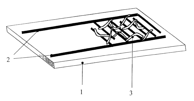
Fig. 1 schematically shows a chemiresistor, which has a sensor medium
comprising
one-dimensional nanoparticles (nanobelts) as a sensitive material. On a
substrate 1 are
placed interdigitated electrodes 2. The electrode structures 2 are covered by
a sensor
film, which is formed of one-dimensional nanoparticles 3. A constant current
may be
applied to the leads of the electrodes 2 and a change in the voltage across
the electrodes
may be detected by a detector (not shown).
Fig. 2 displays different arrangements of one-dimensional nanoparticles 4
between a
pair of electrodes 2. In fig. 2a a single one-dimensional nanoparticle 4 is
bridging the
gap between the pair of electrodes 2. For simplicity only one one-dimensional
nanoparticle is shown on the figure. Several particles can also be employed.
In this
arrangement, the analyte can modulate the conductivity along the one-
dimensional
nanoparticle by adsorption on its surface and/or by intercalation. The analyte
can also
influence the conductivity of the device by affecting the conduction path
between the
particles 4 and the electrodes 2. The arrangement shown in fig. 2a is
preferred for
detecting analytes mainly interacting with the particles changing the
intrinsic
conductivity of the one-dimensional particles. The one-dimensional
nanoparticles can
have a length much smaller than the gap size between a pair of electrodes. The
one-
dimensional nanoparticles are then arranged in a random order to form a
network of
CA 02468251 2004-05-25
WO 03/046536 PCT/EP02/13309
21
nanoparticles 4 between a pair of electrodes 2 as shown in fig. 2b. Like in
the
arrangement of fig. 2a the analyte can affect the intrinsic conductivity of
the particles as
well as the contact resistance between the particles and the electrodes. In
addition, the
analyte can change the interparticle contacts. In this arrangement the analyte
enhances
or reduces the conduction between the nanoparticles. The arrangement shown in
fig. 2b
is preferred when the analyte interacts with the interparticle contacts.
Between
individual one-dimensional nanoparticles 4 are formed voids, which provide an
easy
access of the analyte to the nanoparticle surface even when a sensor medium of
a larger
thickness is used.
Fig. 3 schematically displays a sensor device, which utilizes the influence of
humidity
on the sensitivity of the sensor towards different analytes. In a sample
reservoir 5 an
analyte is provided, comprising various compounds, e.g. an amine and propanol.
From
the sample reservoir 5 the analytes are transported by an carrier gas stream,
e.g. a
nitrogen stream, through a line 6 to a three-way valve 7. In a first step the
three-way
valve 7 is open towards line 6a, whereas line 6b is shut. The gas stream
containing the
analytes is passing a humidity control device 8 by which a defined humidity is
adjusted.
The humidity of the gas stream is monitored by a humidity-monitoring unit 9.
The
humidified gas stream passes a further three-way valve 10 and is then
introduced into
sensor chamber 11, where first signal is detected by sensor 12. Sensor 12 is
connected
to a computer (not displayed), that acts as a detecting device for storing and
comparing
the detected signals. Line 6b is shut by further three-way valve 10 and no gas
is
introduced into line 6b. In a second step three-way valves 7 and 10 are
switched in
such a way that line 6a is shut whereas line f>b is opened. The gas stream
containing
the analytes is now introduced into a drying unit 13 and dried for example by
a drying
agent. The dry gas stream is then introduced into sensor chamber 11 and a
second
signal is detected by sensor 12. In case humidity has little influence on the
sensitivity of
the sensor 12 towards propanol but has a large influence on the sensitivity of
sensor 12
towards amines comparing first and second signal can differentiate those
compounds.
Whereas almost no difference is obtained in case of propanol a clear
difference in
intensity between both signals can be seen in case of an amine.
a) Preparation of undoped vanadium pentoxide nanobelts:
A wet-chemical method previously described by J. Muster et al. Ioc. cit. was
used to
prepare a stock of undoped Vz05 nanofibres. V205 sols were prepared from 0,2 g
ammonium(meta)vanadate (Aldrich) and 2 g acidic ion exchange resin (Dower
50WX8-
CA 02468251 2004-05-25
WO 03/046536 PCT/EP02/13309
22
100, Aldrich) in 40 mL water. After a few hours the formation of an orange sol
is
observed that darkens with time. V2O5 fibres with length of a few micrometers
were
observed after about 3 days. The fibres employed for the experiments were
several
months old.
b) Preparation of silver doped vanadium pentoxide nanobelts
Silver doped vanadium pentoxide nanofibres were prepared as described under
(a) but
during preparation of the Vz05 sols a silver salt (silver nitrate) is added to
the solution.
The silver doped vanadium pentoxide nanofibres were used to prepare sensor 7.
c) Fabrication of sensors:
The one-dimensional nanoparticles were deposited onto BK7 glass substrates
supporting lithographically made interdigitated electrode structures. The
electrode
structures comprised a 5 nm titanium adhesion layer on which a 95 nm gold
layer was
deposited. They comprised 50 finger pairs having a width of 10 ,um, a spacing
of 10 ,um,
and an overlap of 1800 ,um. The overall size of the electrode structures was 2
mm by 2
mm. Before depositing the sensor film, the substrates were cleaned in an
ultrasonic
bath with acetone, hexane, and isopropanol and by applying an oxygen plasma (4
min
at 30 W and 0.24 mbar). The cleaned substrates were immersed into a solution
of 0,1
DAS (N-[3-(trimethoxysilyl)propyl]-ethylenediamine, Aldrich) in water for two
minutes
followed by thorough rinsing with pure water and drying under a stream of air.
This
procedure functionalised the glass substrates with amino groups, which served
as
linking groups for subseduent nanofibre deposition. Fibres obtained under (a)
were dip
coated onto the substrates by dipping the substrate for 20 s in a diluted
suspension of
the fibres in HZO. The substrates were rinsed with pure water and dried in a
stream of
air. Undoped V205-nanofibre sensors (sensor 8) were obtained in this way.
d) Fabrication of a silver-doped sensor (sensor 7)
The fabrication procedure described under (c) was repeated but as one-
dimensional
nanoparticles were used silver doped vanadium pentoxide nanofibres obtained
under
(b). Thereby a silver doped V~05-nanofibre sensor was obtained as sensor 7.
CA 02468251 2004-05-25
WO 03/046536 PCT/EP02/13309
23
e) Doping of sensors by dipping
Sensors obtained under (c) were dipped into a solution of the dopant as
detailed in table
1. After dipping the sensors Were thoroughly rinsed with pure water and dried
in a
stream of air.
Table 1: Sensors obtained by dipping in a dopant solution
Sensor Dopant [Dopant] Solvent Exposure time
1 Silver acetate 1 mg in 1 ml H20 10 s
2 AuS(CH3)2+Cl- 1 mg in 1 ml NMF 20 min
4 AuCl3 1 mg in 1 ml NMF 30 min
5 Silver acetate 0.1 mg in 1 H20 10 s
ml
6 Silver acetate 10 mg in 1 ml H20 10 s
fj Doping of sensor by evaporation of a gold layer (sensor 3)
Evaporation of a gold layer of 2 nm thickness on an undoped sensor obtained
under (c).
resulted in sensor 3. Atomic force microscopy showed that approximately
spherical
particles were formed.
g) Sensitivity of sensors to different gases
For gas test experiments, the sensors prepared as described under (c) - ( fl
were placed
in a home made teflon chamber having a volume of about 1.23 cm3. The test gas
was
prepared by diluting a stock of an analyte (10 % analyte (H2, CO, NH3) in dry
N2) with an
appropriate amount of carrier gas (dry N~) using a mass flow system MK5 from
MCZ
Umwelttechnik GmbH, Ober-Morlen, Germany to obtain the desired analyte
concentration. The mass flow in the test chamber was adjusted to 400 mLJmin
and
kept constant for all experiments. All experiments were done at room
temperature.
The resistance was monitored by applying a do current using a SMU 236
(Keithley) and
recording the voltage using a multimeter 2002 (Keithley). The relative change
in
resistance was measured 120 s after exposing the sensors to the gas of
interest.
CA 02468251 2004-05-25
WO 03/046536 PCT/EP02/13309
24
Table 2: Response ~R/R~i of sensors 1 - 4 to different gases
100 ppm NH3 100 ppm CO 100 ppm H2
Sensor 1 + 18 % + 1.2 % + 0.4
Sensor2 -17% -6% -0.7%
Sensor 3 - g % - 1.2 % - 0.8
Sensor 4 + 13 % + 1.6 % + 0.2
The responses of sensors 1 - 3 are also graphically displayed in fig. 3.
Whereas sensors
1 and 2 have about the same sensitivity to ammonia (in absolute value), sensor
2 has .a
sensitivity towards CO which is about 5 times larger than for sensor 1. By
combining
these two sensors it is therefore possible to distinguish NH3 and CO. Sensor 3
is less
sensitive to ammonia than sensors 1 and 2, but is more sensitive to HZ. This
makes this
sensor more suitable for applications where detection of hydrogen is required.
h) Influence of doping level
Silver doped vanadium pentoxide sensors l, 5 and 6 having low (sensor 5),
medium
(sensor 1 ) and high (sensor 6) doping level were exposed to 100 ppm CO. The
response
of the sensors is displayed in fig. 5. Whereas sensor 5 displayed a fast
response and a
change in relative resistivity OR/R,ni of -1.3 % sensors 1 and 6 having medium
and high
doping level displayed a change in relative resistivity ~R/Rin, of + 1.0 % and
+ 1.3,
respectively. This demonstrates that the response of the sensor can be
modified by
varying the doping level.
i) Sensitivity of silver doped vanadium pentoxide sensors toward NH3
Sensor 7 was exposed to 360 ppb ammonia. The response of the sensor is
displayed in
fig. 6. The sensor displayed a fast response of ~R/R,n, - 1.6 % within 120
seconds. This
demonstrates that the sensor is sensitive to very low concentrations of
ammonia giving
a fast response and a short recovery period. At higher ammonia concentrations
an
increased response of the sensor is obtained as is obvious from the
sensitivity isotherm
displayed in fig. 7.
k) Sensitivity towards carbon monoxide
CA 02468251 2004-05-25
WO 03/046536 PCT/EP02/13309
Gold doped sensor 2 was exposed to 1 ppm CO at room temperature. The response
of
the sensor is displayed in fig. 8. Even at low concentration a response
OR/R,", of - 1.7
was obtained within 120 seconds.
5 1) Sensitivity towards hydrogen gas
Gold doped sensor 3 was exposed to 20 ppm H~ at room temperature. The response
of
the sensor is displayed in fig. 9. Within 120 s a response OR/Rj"i of - 0.4
was obtained.
10 The vanadium pentoxide based sensors can be used as single sensor for NH3,
CO and
H2. Due to the cross-sensitivity to different gases and to the different
selectivities of the
different sensors, an array of V~05-based sensors with different dopants can
be used as
an array of sensors for electronic noses.
15 m) sensitivity towards butylamine at high humidity
Silver doped sensor 7 was exposed to 30 ppb butylamine at 40 % relative
humidity. The
response of the sensor is displayed in fig. 10. The arrow up shows when the
butylamine
is applied and the arrow down shows when the butylamine is removed from the
gas
20 phase. Within 500 s a response ~RIR,°i of 1.9 % was obtained.
n) detection of biogenic amines
Two fresh fish samples (cod) where prepared and stored in glass containers
each. The
25 gas of the head space was sampled by using a micropump and analyzed by
exposing it
to silver doped sensor 7 for 10 seconds each. First sample 1 was analyzed
followed by
sample 2. The dotted line displayed in fig. 11 is the trace recorded at one
day when the
samples were fresh. Both samples gave similar signals. Sample 1 was then
stored in a
fridge for 24 hours whereas sample 2 was stored at ambient conditions. Both
samples
were again analyzed the next day. The plain line displayed in fig. 11
corresponds to the
trace recorded after storage of the samples. The signal of sample 2, stored
under
ambient conditions, gives a larger response than the signal of sample 1 stored
in the
fridge. It is known that most sea fishes produce amines during decomposition.
We
CA 02468251 2004-05-25
WO 03/046536 PCT/EP02/13309
26
assign the increase in signal of sample 2 to a faster decomposition of the
fish due to the
elevated storing temperature, and therefore a higher level of amine.
o) influence of humidity on sensor sensitivity
Silver doped sensor 7 was ea~posed to 237 ppm butylamine at different
humidities. The
sensor response was measured at 5, 20, 30, 40, 50 and 60 % relative humidity.
The
response of the sensor is displayed in fig. 12. The arrow indicates the
increasing
humidity. The highest level of sensitivity was obtained at 60 % relative
humidity.