Note: Descriptions are shown in the official language in which they were submitted.
CA 02468391 2004-05-25
WO 03/049092 PCT/EPO1/15421
A SOLID STATE MICROOPTICAL ELECTROMECHANICAL SYSTEM (MOENS) FOR READING A
PHOTONICS DIFFRACTIVE MEMORY
FIELD OF THE INVENTION
The present invention generally relates to a photonics diffractive memory.
In particular, the present invention relates to an apparatus for reading
information
from the photonics diffractive memory.
BACKGROUND OF THE INVENTION
The large storage capacities and relative low costs of CD-ROMS and DVDs
have created an even greater demand for still larger and cheaper optical
storage
media. Holographic memories have been proposed to supersede the optical disc
as a high-capacity digital storage medium. The high density and speed of the
holographic memory comes from three-dimensional recording and from the
simultaneous readout of an entire packet of data at one time. The principal
advantages of holographic memory are a higher information density (10" bits or
more per square centimeter), a short random access time ( ~ 100 microseconds
and
less), and a high information transmission rate (109 bit/sec).
In holographic recording, a light beam from a coherent monochromatic source
(e.g., a laser) is split into a reference beam and an object beam. The object
beam
is passed through a spatial light modulator (SLM) and then into a storage
medium.
1
CA 02468391 2004-05-25
WO 03/049092 PCT/EPO1/15421
The SLM forms a matrix of shutters that represents a packet of binary data.
The
object beam passes through the SLM which acts to modulate the object beam with
the binary information being displayed on the SLM. The modulated object beam
is
then directed to one point on the storage medium by an addressing mechanism
where it intersects with the reference beam to create a hologram representing
the
packet of data.
An optical system consisting of lenses and mirrors is used to precisely direct
the optical beam encoded with the packet of data to the particular addressed
area
of the storage medium. Optimum use of the capacity of a thick storage medium
is
realized by spatial and angular multiplexing. In spatial multiplexing, a set
of packets
is stored in the storage medium shaped into a plane as an array of spatially
separated and regularly arranged subholograms by varying the beam direction in
the x-axis and y-axis of the plane. Each subhologram is formed at a point in
the
storage medium with the rectangular coordinates representing the respective
packet
address as recorded in the storage medium. In angular multiplexing, recording
is
carried out by keeping the x- and y- coordinates the same while changing the
irradiation angle of the reference beam in the storage medium. By repeatedly
incrementing the irradiation angle, a plurality of packets of information is
recorded
as a set of subholograms at the same x- and y- spatial location.
Previous holographic devices for recording information in a highly
multiplexed volume holographic memory, and for reading the information out,
2
CA 02468391 2004-05-25
WO 03/049092 PCT/EPO1/15421
require components and dimensions having a large size which places a limit on
the
ability to miniaturize these systems. Because previous holographic devices use
motors and large-scale components such as mirrors and lenses, the addressing
systems of these previous devices are slow. Furthermore, the mechanical
components of these previous devices need frequent maintenance to correct
errors
and dysfunction coming, for instance, from wear and friction (i.e., tribology
effect).
Furthermore, previous addressing systems are expensive because they use
complex systems for control. Thus, their prices cannot be lowered by mass
production. Moreover, previous devices are not economical in their energy
consumption. Even when previous addressing devices are accurate when new, the
wear and friction of the interacting surfaces that are in relative motion
lowers their
accuracy with time.
In view of the foregoing, it would be desirable to provide one or more
techniques which overcomes the above-described inadequacies and shortcomings
of the above-described proposed solutions.
OBJECTS OF THE INVENTION
In view of the foregoing, it is an object of the present invention to provide
an
improvement in higher speed and smaller size of photonics diffractive memory
reading systems.
It is a further object of the present invention to provide a miniaturization
of a
3
CA 02468391 2004-05-25
WO 03/049092 PCT/EPO1/15421
photonics diffractive memory reading system.
It is another object of the present invention to reduce the addressing system
of a photonics diffractive memory reading system to a matchbox size.
It is a still a further object of the present invention to design a solid
state
reading system that can be rapidly manufactured in large quantities and low
cost out
of existing resources.
SUMMARY OF THE INVENTION
In order to achieve the above-mentioned objectives, the present invention
comprises a solid-state system for reading information from a photonics
diffractive
memory. A coherent light source generates a convergent light beam which is
then
deflected by an acousto-optic deflector. A plurality of micro-mirrors receives
the
deflected light beam from the acousto-optic deflector at one of the micro-
mirrors.
A photonics diffractive memory having a plurality of points receives at one of
the
points the reflected light beam which is reflected from the micro-mirror. A
detector
has a plurality of light-detecting cells. At least one of the cells receives a
portion of
the reflected light beam transmitted through the point.
In a further aspect of the present invention, the micro-mirrors are configured
as a matrix.
In another aspect of the present invention, there is a lens which forms the
4
CA 02468391 2004-05-25
WO 03/049092 PCT/EPO1/15421
convergent light beam from the light source.
In still another aspect of the present invention, the convergent light source
is selected from the group consisting of a low power laser and a light-
emitting diode.
In yet another aspect of the present invention, the detector is a CCD
detector array.
In a further aspect of the present invention, each of the plurality of points
stores one or more diffraction patterns.
In yet another aspect of the present invention, the photonics diffractive
memory comprises stored therein information located at the plurality of points
of the
memory and at a plurality of angles at each one of the points so as to form a
plurality of packets of information at each one of the points.
In another aspect of the present invention, each of the micro-mirrors is a
oscillatory scanning micro-mirror.
In a further aspect of the present invention, a computer is configured to
coordinate the synchronization of the acousto-optic deflector and the
oscillatory
micro-mirrors so that the reflected light beam is directed to one of the
points with a
specific angle for a sufficient time to retrieve information from the point.
In yet another aspect of the present invention, each of the micro-mirrors is
a oscillatory micro-mirror and the oscillation cycle of the micro-mirror is
coordinated
with the scanning of the acousto-optical deflector so as to direct said
reflected light
beam onto one of the points of the storage medium.
5
CA 02468391 2004-05-25
WO 03/049092 PCT/EPO1/15421
BRIEF DESCRIPTION OF THE DRAWINGS
In order to facilitate a fuller understanding of the present invention,
reference
is now made to the appended drawings. These drawings should not be construed
as limiting the present invention, but are intended to be exemplary only.
FIG. 1 shows a micro-mirror assembly according to the present invention.
FIG. 2 shows a perspective view of a micro-mirror assembly according to the
present invention.
FIG. 2a shows a close up view of the actuator of the micro-mirror assembly
according to the present invention.
FIG. 3a shows adding an epitaxial layer to a wafer as part of the MEMS
fabrication process according to the present invention.
FIG. 3b shows the formation of the starting electrodes and deposition of a
metal layer as part of the MEMS fabrication process according to the present
invention.
FIG. 3c shows an anisotropical etch to remove the substrate underneath the
designed mirror plate as part of the MEMS fabrication process according to the
present invention.
FIG. 3d shows a cross section of the micro-mirror chip according to the
present invention.
FIG. 4a shows a starting electrode of a micro-mirror assembly according to
6
CA 02468391 2004-05-25
WO 03/049092 PCT/EPO1/15421
the present invention.
FIG. 4b shows operation of a micro-mirror being driven by a saw tooth signal
according to the present invention.
FIG. 5 shows a solid state reading system according to the present invention.
FIG. 6 shows an acousto-optic deflector according to the present invention.
FIG. 7 shows a schematic representation of a diffractive optics recording
process
FIG. 8 shows a matrix of points forming a storage medium according to the
present invention.
FIG. 9 shows synchronization of the mirror of the solid state reading system
according to the present invention.
DETAILED DESCRIPTION OF THE INVENTION
The compact architecture for diffractive optics systems in accordance with
the present invention integrates a number of components into a compact
package, including an acousto-optic deflector and a microoptoelectromechanical
system (MOEMS) device which reduces the addressing component of a reading
system for a photonics diffractive memory to a matchbox size. The reading
system is made of solid-state components. The mirrors are built in CMOS
technology resulting in the advantage that the reading system can be mass-
produced at low cost.
7
CA 02468391 2004-05-25
WO 03/049092 PCT/EPO1/15421
Various diffractive recording/reading processes have been developed in the
art and further details can be found in the book Holographic Data Storage,
Springer
(2000) edited by H.J. Coufal, D. Psaltis, and G.T. Sincerbox. In this
specification,
the term "diffractive" is used throughout to differentiate prior art
holographic
technology used for 3-D image generation from diffractive technology necessary
for
the generation of a storage medium. For example, diffraction efficiency is
critical
to the viability of any material to be used as a diffractive storage medium.
The
quality of interference constituting a 3D-hologram is simple to achieve
compared to
the quality required to realize a storage medium. Moreover, a storage
diffractive
pattern can also be implemented by using other techniques than the
interference
of a reference and object beam, such as using as an e-beam etched on a
material
to generated diffraction patterns. For all these reasons, the specification
herein
introduces the concept of a broader diffractive optics technology.
FIG. 1 shows a top view of a scanning micro-mi,rrorelement 100 comprising
a mirror plate 102 suspended by two or four torsional springs 122a, 122b which
connect the mirror plate 102 to anchors 120a, 120b, respectively. The anchors
120a, 120b are attached to the substrate 110. The two comb like driving
electrodes
105a, 105b create torque to move the mirror plate 102. The mirror plate 102 of
FIG.
1 is an example of a microoptoelectromechanicalsystem (MOEMS). A MEOMS is
a system which combines electrical and mechanical components, including
optical
components, into a physically small size.
8
CA 02468391 2004-05-25
WO 03/049092 PCT/EPO1/15421
FIG. 2 shows a perspective view of the micro-mirror element 100 comprising
the mirror plate 102 cut in a silicon substrate on which a reflected film is
deposited,
typically a film of aluminum with a typical thickness of about fifty
nanometers. The
plate 102 is suspended from the two or four twisting points 120a, 120b and is
actuated by the two or four drive electrodes 105a, 105b, depending on whether
it
is desired to have the mirror 102 rotates in one or two directions. The angle
of
deflection is in theory unlimited, but in practice it is about 60°.
The variation of the capacitance C 125 (C varies with angle ~) between the
mirror plate 102 and the comb like driving electrodes 105a, 105b is used to
generate the plate tortional movement. If a voltage U is applied by an energy
source (not shown) to the driving electrodes 105a, 105b, the generated
electrostatic
torque M is:
M=1/2dC/dcpU2
where ~ is the deflection angle of the plate.
The mirror plate 102 can have a size from .5 x .5 mm up to 3 x 3 mm. The
actuators (the movement between mirror plate 102 and electrodes 105 as driven
by
the energy source) are resonantly excited, i.e., they are continuously
oscillating.
The scan frequency depends on the size of the mirror plate (0.14KHz up to
20KHz)
and a mechanical scan angle of ~15° can be achieved at a driving
voltage of only
9
CA 02468391 2004-05-25
WO 03/049092 PCT/EPO1/15421
20V.
When the actuator works in synchronous mode, it is possible to control the
angular position of the mirror plate 102 by controlling the maximum deflection
amplitude and oscillating period. Advantages of these mirrors is that the
amplitude
of the deflection can be monitored with the driving voltage U. For a large
scan
angle, the deflection angle varies linearly with the excitation voltage.
As shown in FIG 2A, the space lying between the mirror plate 102 and the
drive electrodes 105a, 105b forms a variable capacitor. Thus, applying a
voltage
generates electrostatic torque acting on the plate and causing it to rotate
and/or
oscillate. Given the particularly small size of these micro-mirrors on the one
hand,
but also their mode of operation on the other, it becomes possible to reduce
the size
of the read device 400 (see FIG. 5) significantly and hence achieve a very
high level
of integration.
FIGs. 3a-3d show the process for manufacturing a micro-mirror element
200 on a substrate 230 with starting electrodes 210a, 210b. The fabrication is
achieved using a CMOS-compatible technology. Referring to FIG. 3a, a wafer
230 serves as the base material. A buried oxide (BOX) layer 221 is produced in
a SIMOX (Separation by Implantation of Oxygen) process. A 200-nm-thick
silicon layer 205 on top of the BOX 221 is strengthened by a 20 um thick
epitaxial layer. Referring to FIG. 3b, an oxide and a metal layer are
deposited
and patterned to form the starting electrodes 210a, 210b. The metal layer is
CA 02468391 2004-05-25
WO 03/049092 PCT/EPO1/15421
protected by an additional oxide. In the next step a 50-nm-thick layer 206 of
AI is
deposited forming the reflective coating in the mirror area. Referring to FIG.
3c.,
the substrate underneath the designed torsional springs and the mirror plate
205
is removed by an anisotropical etch in a tetramethylammonium hydroxide
(TMAH) solution leaving the remaining portions 230. TMAH is a chemical
solution used for antisotropical etching of the wafer substrate in which the
micro
mirrors are etched. After that the BOX layer is removed and the epitaxial
layer is
patterned using the Advanced Silicon EtchT""-process, trenches 207 are formed.
A cross section of the micro-mirror chip 200 at the end of the process is
shown in
Figure 3d.
FIG. 4a illustrates the operation of the micro-mirror element 100. FIG. 4a
shows the starting electrodes 210a used to start a motion of the mirror plate
205.
A voltage of a fixed frequency is applied on the starting electrode 210a which
yield asymmetries. Assuming perfect symmetry of the actuator it is impossible
to
start the oscillation without external induced forces. Therefore, there is an
additional starting electrode 210a, 210b which is located on top of each of
the
driving electrodes 221 and isolated from it by an oxide 209. These electrodes
210a, 210b can be contacted separately and break the symmetry of the
configuration. Once oscillation is initiated, the mirror actuation works in a
synchronized mode where the mirror plate 205 oscillates in phase with the
driving excitation of the voltage U generated by an energy source.
11
CA 02468391 2004-05-25
WO 03/049092 PCT/EPO1/15421
FIG. 4b shows synchronization of the mirror plate 102 as driven by a saw
tooth signal 300. The saw tooth signal 300 comprises the voltage U applied
with a predetermined frequency per second. The operation of the mirror plate
102 is shown at five different positions 301-305 as the mirror plate 102 is
driven
by saw tooth wave 300 applied across the drive electrodes 105a, 105b (see FIG.
1). In a full cycle comprising a movement from a positive angle, to zero
degrees,
to a negative angle, the mirror element 102 moves from positions 301 to 304 (a
full cycle) and then begins the cycle again at position 305.
Table 1 shows the eigenfrequency (resonance frequency) of the micro-
mirror element 100 as a function of mirror size. The eigenfrequency depends on
the mechanical and electrical characteristics of the micro-mirror element 100.
In
the synchronized mode, the mirror oscillates at two times the eigenfrequency.
1 D Mirror0.5 1 1.5 2 3
size (mm)
Resonance 2.32 0.4 - 7.5 .25 - 2.5 .14 - 1.5 .2
frequency
(Khz)
Table 1
12
CA 02468391 2004-05-25
WO 03/049092 PCT/EPO1/15421
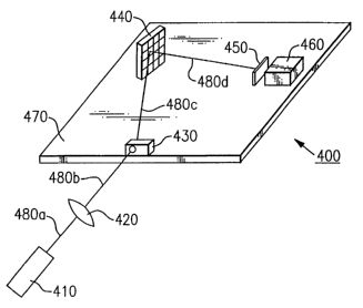
FIG. 5 shows a reading system 400 comprising a separate unit on a
platform 470 supporting an acousto-optic deflector 430, a
microoptoelectromechanical systems (MOEMS) matrix 440, a matrix memory
450, and an image sensor 460, such as a CCD (charge-coupled device)
detection system or other such image detection system. Additional devices
located on or off the platform 470 comprise a light source 410 (e.g., a laser,
laser
diode) and a converging lens 420.
The operation of the reading system proceeds with the light source 410
emitting a light beam 480a which is focused by the converging lens 420 from a
plane wave to spherical wave 480b. The spherical wave 480b is a convergent
beam. The convergent beam 480b is deflected by the acousto-optic deflector 430
to form beam 480c which impinges on one of the micro-mirror elements of the
MEOMS matrix 440. The MEOMS mirror matrix 440 has a size that fits the
constraints of the memory matrix addressing system. The matrix of micro-
mirrors
440 is used to address the matrix of points of the memory 450 in which data
are
recorded by spatial and angular multiplexing. The beam 480c coming from the
acousto-optic deflector 430 forms an area with a diameter that can fit within
the
diameter of each one of the mirror elements of the MEOMS matrix 440.
Additionally, the memory matrix 450 is spatially adjusted in such a way that
the size
of the laser beam 480d fits exactly the size of every point of the memory
matrix 450.
13
CA 02468391 2004-05-25
WO 03/049092 PCT/EPO1/15421
FIG. 6 shows the acousto-opticdeflector430 in greater detail. The acousto-
optic (AO) deflector 430 directs the laser beam 480b at an angle to the micro-
mirror
array 440. When acousto-optical crystals are subjected to stress, especially
by
means of a transducer usually consisting of a piezoelectric crystal, they
modify the
angle of diffraction of the light and, in general, of the electromagnetic wave
which
passes through them in order to modify the value of the diffraction angle of
the
emerging beam 480c. Thus, modifying the actuating frequency of the
piezoelectric
transducer deflects the light beam 480b to form the light beam 480c at one of
a
plurality of angles.
Thus, as shown in FIG 6, the variations in orientation along OX and OY
(referring to the rectilinear co-ordinates of FIG. 2) of the incident read
beam 480b
emanating from the low-power laser 410 are obtained by subjecting this beam to
two acousto-optic components 121, 122. Consequently it may be understood that,
by varying the vibration frequency of the piezoelectric crystal associated
with the
acousto-optic component(s), it becomes possible to modify, very rapidly, the
desired
orientation of the grating within the rows and columns of the data-carrying
matrix
450. The limiting factor then becomes the response time of the mirror elements
of
the MEOMS matrix 440 which act on the angle of incidence of the read beam.
FIG. 7 and FIG. 8 describe the contents of the diffractive storage medium.
Referring to FIG. 7, in forming a diffractive pattern, or alternately a
hologram, a
reference beam 1 intersects with an object beam 4 to form a sub-hologram 8a
14
CA 02468391 2004-05-25
WO 03/049092 PCT/EPO1/15421
(referred to alternately as a point) extending through the volume of storage
medium
8. There is a separate sub-hologram or point 8a extending through the volume
for
each angle and spatial location of the reference beam 1. The object beam 4 is
modulated with a packet of information 6. The packet 6 contains information in
the
form of a plurality of bits. The source of the information for the packet 6
can be a
computer, the Internet, or any other information-producing source. The
hologram
impinges on the surface 8a of the storage medium 8 and extends through the
volume of the storage medium 8. The information for the packet 6 is modulated
onto the storage medium 8 by spatial multiplexing and angle multiplexing.
Angle
multiplexing is achieved by varying the angle a of the reference beam 1 with
respect
to the surface plane of the storage medium 8. A separate packet 6 of
information
is recorded in the storage medium 8 as a sub-hologram for each chosen angle a
and spatial location. Spatial multiplexing is achieved by shifting the
reference beam
1 with respect to the surface of the storage medium 8 so that the point 8a
shifts to
another spatial location, for example point 8a', on the surface of the storage
medium 8.
The storage medium 8 is typically a three-dimensional body made up of a
material sensitive to a spatial distribution of light energy produced by
interference
of the object light beam 4 and the reference light beam 1. A hologram may be
recorded in a medium as a variation of absorption or phase or both. The
storage
material must respond to incident light patterns causing a change in its
optical
CA 02468391 2004-05-25
WO 03/049092 PCT/EPO1/15421
properties. In a volume hologram, a large number of packets of data can be
superimposed, so that every packet of data can be reconstructed without
distortion.
A volume (thick) hologram may be regarded as a superposition of three
dimensional gratings recorded in the depth of the layer of the recording
material
each satisfying the Bragg law (i.e., a volume phase grating). The grating
planes in
a volume hologram produce change in refraction and/or absorption.
Several materials have been considered as storage material for optical
storage systems because of inherent advantages. These advantages include a
self developing capability, dry processing, good stability, thick emulsion,
high
sensitivity, and nonvolatile storage. Some materials that have been considered
for
volume holograms are photorefractive crystals, photopolymer materials, and
polypeptide material.
Referring now to FIG.B, there is shown in greater detail the storage medium
8 arranged in the form of a flat sheet, herein referred to as a matrix. In
this
example, the matrix is 1 cm2. Each of a plurality of points on the matrix is
defined
by its rectilinear coordinates (x, y). An image-forming system (not shown)
reduces
the object beam 4 to the sub-hologram 8a having a minimum adopted size at one
of the x, y point of the matrix. A point in physical space defined by its
rectilinear
coordinates contains a plurality of packets 8b.
In this case, a 1 mm2 image 8a is obtained by focusing the object beam 4
onto the storage medium 8 centered at its coordinate. Due to this interference
16
CA 02468391 2004-05-25
WO 03/049092 PCT/EPO1/15421
between the two beams 1,4, a diffractive image 8a 1 mm2 in size is recorded in
the
storage material 8 centered at the coordinates of the matrix. Spatial
multiplexing
is carried out by sequentially changing the rectilinear coordinates. The
object beam
4 focuses on the storage material 8 so that a separate image 8a is recorded at
a
5. unique position in the plane defined by its coordinates (x, y). This
spatial
multiplexing results in a 10 by 10 matrix of diffractive images 8a. Angle
multiplexing
is carried out by sequentially changing the angle of the reference beam 1 by
means
of the mirror elements of the MEOMS matrix 440. Angle multiplexing is used to
create 15-20 packets of information 8b corresponding to 15 discrete variations
of
the angle of incidence of the reference beam. Additionally, it is possible to
reach
20-25 packets by simple multiplexing and 40-50 packets by using double
symmetrical angular multiplexing. A data packet is reconstructed by shinning
the
reference beam 1 at the same angle and spatial location in which the data
packed
was recorded. The portion of the reference beam 1 diffracted by the storage
material 8 forms the reconstruction, which is typically detected by a detector
array.
The storage material 8 may be mechanically shifted in order to store data
packets
at different points by its coordinates (x, y).
FIG. 9 shows synchronization of the micro-mirrors 440. Because the
micro-mirrors 440 are continuously oscillating, it is necessary to synchronize
the
acousto-optic deflector (AOD) 430 and the micro-mirrors 440 in order to
realize
the addressing of a data packet of the memory 450. By knowing mirrors
17
CA 02468391 2004-05-25
WO 03/049092 PCT/EPO1/15421
parameters like amplitude of deflection and oscillating period, it is possible
to
control the switching time of the AOD 430. This way, one of the micro-mirrors
can be accessed which addresses a desired position on the memory 450. The
AOD 430 redirects the laser beam on a chosen mirror at a given time.
Two representative micro-mirrors 440a, 440b of the micro-mirror array 440
of FIG. 5 are shown with each of the micro-mirrors at a different position.
The
rest position 441 a is shown for the micro-mirror 440a. The rest position 441
b is
shown for the micro-mirror 440b. The coherent laser beam.is directed by the
AOD 430 at different times to one of the micro-mirrors 440a, 440b which
reflect
the light beam at a predetermined location and angle to the memory 450. The
lens 455 focuses the light energy onto the CCD array 460. A CPU (not shown),
such as a computer, microcontroller, or other such control device, controls
the
AOD 430, the micro-mirrors 440, and the CCD detector 460. The CPU (not
shown) receives inputs from sensors indicating the positions of the micro-
mirrors
440a, 440b and receives inputs on the state of the AOD 430. The CPU (not
shown) then controls the mirror positions of the micro-mirrors 440 and the
deflection angle of the AOD 430. Synchronization of the micro-mirrors 440 with
the AOD 430 is necessary to reach a maximum deflection angle. The maximum
deflection angle is the maximum angle that can be reached by the processed
beam. This means that the output beam of the acousto-optic device can reach a
maximum value. Between the positive and negative value of this maximum will
18
CA 02468391 2004-05-25
WO 03/049092 PCT/EPO1/15421
lie the angular range of the acousto-optic device. An other advantage of
synchronization is that the maximum deflection can be monitored by the driving
voltage control . That is, the deflection varies linearly with the driving
excitation
voltage U.
FIG. 9 illustrates synchronization between the micro-mirrors 440, the AOD
430 and the CCD camera 460. The synchronization is shown for two of the
micro-mirrors 440a, 440b of the micro-mirror array 440. Because the micro-
mirrors 440a, 440b are continuously oscillating at low frequencies (i.e.,
200Hz),
the micro-mirrors 440a, 440b can be considered as fixed mirrors compared to
the switching time of the AOD (10 to 100 ~ s). At a switching time T, the
micro-
mirrors positions can be monitored so that the it is determined how to access
a
specific packet of information from the memory 450. In the present invention,
the
CPU (not shown) controls the mirror synchronization and calculates the
switching time of the AOD 430 and the CCD 460 to read a given packet of the
memory 450. The positions of the micro-mirrors 440 are calculated to address
every packet of the memory 450. At a time T1, the AOD 430 is switched to
address the micro-mirror 440a to read a packet of the memory 450. At another
time T2, the AOD 430 is switched to address the micro-mirror 440b to read a
packet of the memory 450. The micro-mirror 440a is shown at an angle a1 from
the normal position 441 a. The micro-mirror 440b is shown at an angle a2 from
the normal position 441 b. The lens 455 focuses the output waveform carrying
19
CA 02468391 2004-05-25
WO 03/049092 PCT/EPO1/15421
the data packets onto the array of the CCD camera 460.
The present invention is not to be limited in scope by the specific
embodiments described herein. Indeed, various modifications of the present
invention, in addition to those described herein, will be apparent to those of
skill in
the art from the foregoing description and accompanying drawings. Thus, such
modifications are intended to fall within the scope of the appended claims.
20