Note: Descriptions are shown in the official language in which they were submitted.
CA 02468551 2004-05-27
MULTIPART ELECTRONIC CIRCUIT ASSEMBLY WITH DETACHABLY
INTERCONNECTING AND LOCKING COMPONENT CIRCUIT SUBSTRATES
FIELD OF THE INVENTION
The present invention relates generally to the field of electronic circuit
substrates
and more particularly, to an electronic circuit assembly have two or more
component
substrates that detachably interconnect and lock to one another.
BACKGROUND OF THE INVENTION
Electronic equipment conventionally comprises an enclosure such as a box-
shaped housing containing electronic circuitry. In some instances, a face of
such a
housing is open so as to provide access to shelves, each of which may be
configured with
receiving stations for holding electronic circuitry units or circuit packs in
a side-by-side
or top-to-bottom relationship. Typically, such units comprise at least one
circuit substrate
such as a printed circuit board or card carrying a plurality of electronic
components.
When installed into such a housing, one or more of these units may be
connected to
electrical connectors mounted within the housing. Each of the electronic
circuitry units
may provide particularized or dedicated functionality for the end user, and
this may
permit the user to configure a given housing in a modular or customized
manner.
In certain types of electrical equipment, for instance in telecommunications
networking equipment, it would be desirable to have a mechanism that would
permit two
or more circuit substrates such as printed circuit boards to be releasably
interconnected
together. Such an arrangement would allow for various configurations of
printed circuit
boards to be interchanged with each other in a given enclosure therefor.
Moreover, it
would be desirable to have a mechanism that would permit two or more component
circuit substrates such as printed circuit boards to be releasably
interconnected together in
123081-344262
TDO-RED #8232498 v. I
CA 02468551 2004-05-27
-2-
a multipart circuit assembly while permitting one of the boards to be removed
from a
given enclosure therefor and the other of the boards to remain installed and
operational
therein. It would moreover be desirable to have a mechanism that would permit
the said
two or more component circuit substrates to be removed from a given enclosure
therefor
either as an interconnected unit or with one of the component circuit
substrates being
removable therefrom independently of the component circuit substrates to which
the
removable component circuit substrate may be attached.
It is therefore an object of the present invention to provide a mechanism
which
would permit two or more component circuit substrates to be releasably
interconnected
together, such that at least one of said component circuit substrates was
removable from
an enclosure therefor independently of the other component substrates to which
the
removable component substrate may be connected.
These and other objects of the present invention will be made apparent by way
of
the description of the invention which follows.
SUMMARY OF THE INVENTION
According to a first broad aspect of the present invention, there is provided
an
assembly of releasably interconnected circuit substrates, the assembly
comprising: (a) a
first and second circuit substrate, each circuit substrate respectively
providing a first and
second electrical connector for mating electrical engagement between the first
and second
circuit substrates; (b) a two-position lock being operable between a first
position
according to which the first and second circuit substrates are in locked
interconnection
with each other and a second position according to which the first and second
circuit
substrates are separable from each other.
123081-344262
TDO-RED #8232498 v. 1
CA 02468551 2004-05-27
-3-
BRIEF DESCRIPTION OF THE DRAWINGS
For a better understanding of the present invention and to show more clearly
how
it may be carried into effect, reference is now made, by way of example only
and not of
limitation, to the accompanying drawings in which:
FIGURE 1 is a perspective view of a shelf of an equipment housing in which a
multipart interconnected circuit assembly according to an illustrative
embodiment of the
present invention has been deployed (a panel adjacent to the interconnected
circuit
assembly having been removed from the housing for sake of clarity);
FIGURE 2 is an elevation view of the shelf of the housing of Fig. 1, with the
multipart interconnected circuit assembly of Fig. 1 being deployed therein;
FIGURE 3 is another elevation view of the shelf of the housing of Fig. 1,
transverse to the view of Fig. 2, wherein the multipart interconnected circuit
assembly
according to the present invention has not been deployed therein;
FIGURE 4 is another elevation view of the shelf of the housing of Fig. 1, in
the
same direction as the view of Fig. 2, in which a first component substrate of
the multipart
circuit assembly has been releasably detached from a second component circuit
substrate
thereof which remains electrically connected to the shelf;
FIGURE 5 is a perspective view of a first component circuit substrate of the
multipart interconnected circuit assembly according to an embodiment of the
present
invention, wherein the first component circuit substrate is shown detached and
apart from
a second component circuit substrate thereof;
FIGURE 6 is a side elevation view of the first component circuit substrate of
Fig.
5;
123081-394262
TDO-RED #8232998 v. 7
CA 02468551 2004-05-27
-4-
FIGURE 7 is an end elevation view of the first component circuit substrate of
Figs. 5 and 6;
FIGURE 8 is a perspective view of a second component circuit substrate of the
multipart interconnected circuit assembly according to an embodiment of the
present
invention, wherein the second component circuit substrate is shown detached
and apart
from the first component circuit substrate thereof of Figs. 5, 6 and 7;
FIGURE 9 is an end elevation view of the second component circuit substrate of
Fig. 8, showing an end thereof which mates electrically with the first
component circuit
substrate of Figs. 5, 6 and 7;
FIGURE 10 is a side elevation view of the second component circuit substrate
of
Fig. 8 and 9;
FIGURE 11 is another end elevation view of the second component circuit
substrate of Figs. 8, 9 and 10, showing an end thereof which mates
electrically with the
shelf of the enclosure of Figures 1 to 4;
FIGURE 12 is an exploded perspective view of the first component circuit
substrate of Figs. 5 to 7 and the second component circuit substrate of Figs.
8 to 11,
wherein a daughter card of the first component circuit substrate has not been
illustrated so
as to highlight interconnection features of the multipart interconnected
circuit assembly
of Fig. 1;
FIGURE 13 is another perspective view of the first and second component
circuit
substrates of Fig. 12, wherein the said substrates are shown interconnected to
one
another;
/23081-344262
TDO-RED #8232498 v. l
CA 02468551 2004-05-27
- 5 -
FIGURE 14 is a side elevation view of the first and second component circuit
substrates in their interconnected configuration of Fig. 13, wherein a portion
of a locking
mechanism provided with the first component circuit substrate has been
phantomed for
sake of illustration;
FIGURE 15 is a side elevation view of the multipart interconnected circuit
assembly of Fig. 1, wherein both the first component circuit substrate of
Figs. 5 to 7 and
the second component circuit substrate of Figs. 8 to I 1 are shown
interconnected
together, and wherein certain components and parts thereof have not been
illustrated so as
to highlight interconnection features thereof;
FIGURE 15a is a cross-sectional end view showing a detail of interconnection
between the first component circuit substrate of Figs. 5 to 7 and the second
component
circuit substrate of Figs. 8 to 11, namely the engagement of a leading edge of
the first
component circuit substrate with a guide channel provided on the second
component
circuit substrate;
FIGURE I Sb is a cross-sectional end view showing another detail of
interconnection between the first component circuit substrate of Figs. 5 to 7
and the
second component circuit substrate of Figs. 8 to 11, namely the engagement of
a guide
frame provided on the first component circuit substrate with a guide arm
provided on the
second component circuit substrate;
FIGURE 16a is an exploded perspective view of the first component circuit
substrate of Figs. 5 to 7 and the second component circuit substrate of Figs.
8 to 11,
wherein certain components and parts thereof have not been illustrated so as
to highlight
interconnection features of the multipart interconnected circuit assembly of
Fig. 1;
FIGURE 16b is another exploded perspective view of the first and second
component circuit substrates of Figs 5 to 7 and Figs. 8 to 11 respectively,
wherein the
723087-344262
TDO-RED #8232498 v. I
CA 02468551 2004-05-27
-6-
circuit substrates are aligned generally transversely to their direction of
alignment in Fig.
16a;
FIGURE 17 is a side elevation view of the multipart interconnected circuit
assembly of Fig. 1, wherein both the first component circuit substrate of
Figs. 5 to 7 and
the second component circuit substrate of Figs. 8 to 11 are shown
interconnected together
and wherein certain components and parts thereof have not been illustrated so
as to
highlight features of the locking mechanism thereof;
FIGURE 18 is a partial exploded perspective view of the first component
circuit
substrate of Figs. 5 to 7, showing details of the locking mechanism of the
multipart
interconnected circuit assembly of Fig. 1; and
FIGURES 19 and 20 are each a partial side elevation view of the first and
second
component circuit substrates of Figs. S to 7 and of Figs. 8 to 11
respectively, in their
interconnected configuration, and showing further details of the locking
mechanism of
the multipart interconnected circuit assembly of Fig. 1.
DETAILED DESCRIPTION OF EMBODIMENTS
The description which follows, and the embodiments described therein, are
provided by way of illustration of an example or examples of particular
embodiments
which reflect principles of the present invention. These examples are provided
for
purposes of explanation, and not of limitation, of those principles and of the
invention. In
the description which follows, like parts are marked throughout the
specification and the
drawings with the same respective reference numerals.
Referring to Figure 1, there is shown an electrical housing 30 which may be of
the
type known and used in telecommunications switching equipment. The housing 30
is a
123081-349262
TDO-RED #8232498 v. I
CA 02468551 2004-05-27
generally rectangular enclosure that has outer panels 32, 34 and 36. Each of
the outer
panels 32, 34 and 36 is attached to a backplane 38, which is described in
greater detail
below. An additional outer panel (not shown for clarity) extends from the
backplane 38,
as at edge 40 thereof. The housing 30 is open at one face thereof to provide
access to one
or more circuit substrate receiving stations in the form of shelves 42. Each
shelf 42
comprises, in conventional fashion, a set of first and second longitudinal
guides 44 and
46 which are generally disposed in opposed relation to one another.
In the illustrative embodiment, each opposed pair of guides 44 and 46 are
generally coplanar and each shelf 42 measures approximately 20 inches from the
first
guide 44 to the second guide 46. First and second guides 44 and 46 extend in a
direction
generally transverse to the backplane 38 of the housing 30 and serve to direct
the
insertion and removal of electronic circuitry units or circuit packs, such as
the multipart
interconnected circuit assembly 2 or its separable component circuit
substrates 2A and
2B, all as explained in greater detail below.
Once installed in the manner described below, the component circuit substrates
2A and 2B electrically interconnect with respective electrical connectors 54
and 56 (Fig.
3) provided with backplane 38. Electrical connectors 54 and 56 may be known
pin type
connectors with press fit headers. Additionally, backplane 38 may be provided
with
known connectors in the form of power pins 58 (Fig. 3). Power pins 58 provide
an
electrical ground or EDG (Electrical Dumping Ground) to the mounted multipart
interconnected circuit assembly 2, and the mounted component substrate 2B
thereof when
the latter is separate therefrom, to prevent surges of static electricity.
Backplane 38 has a stiffener member or bar 48 which extends across the center
thereof and tends to discourage deflection therein so that proper electrical
connection
may be achieved with the multipart interconnected circuit assembly 2 or its
component
circuit substrates 2A and 2B. As well, the stiffener bar 48 serves an
alignment function
and provides a fastening point for component circuit substrate 2B as explained
below.
723081-344262
TDO-RED #8232498 v. I
CA 02468551 2004-05-27
Housing 30 also has first and second cross-members 50 and 52 which extend
between the
free terminal edges of two opposed outer panels, for instance the outer panels
32 and 36.
Cross-members 50 and 52 provide attachment sites to which the multipart
interconnected
circuit assembly 2 may be fastened during installation thereof into housing
30.
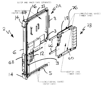
Turning now to Fig. 5, the first component circuit substrate 2A of the
multipart
interconnected circuit assembly 2 according to an embodiment of the present
invention
will next be described. In the embodiment herein described, the multipart
interconnected
circuit assembly 2 provides two interconnected component circuit substrates 2A
and 2B,
but those skilled in this art will appreciate that the present invention is
adaptable to
multipart interconnected circuit assemblies 2 having more than two such parts.
The first
component circuit substrate 2A comprises a printed circuit board or card 4, to
which may
be mounted a plurality of electronic components (not shown), and further
comprises a
transverse web, such as a faceplate 6, adjacent an edge of the printed circuit
card 4 such
that the faceplate 6 will be in external view to a user thereof when the first
component
circuit substrate is mounted in operation within the enclosure 30.
In addition to the printed circuit card 4, the first component circuit
substrate 2A
also provides a daughter card 10 that is spaced apart from the printed circuit
card 4, for
instance in a substantially parallel relationship thereto. As best shown in
Fig. 12, the
daughter card 10 may be attached to the circuit board 4 by means of spacer
pins 3 and a
guide frame 5, by way of example. The guide frame 5 extends generally
transversely
from faceplate 6 adjacent one terminal end thereof and provides an attachment
edge 5a
(Fig. 15b) that extends generally parallel to the printed circuit card 4 and
to which
daughter card 10 may be secured with suitable fasteners 7 or the like (Figs. 5
and 6).
Another function of guide frame 5 will be described hereinbelow.
Daughter card 10 presents a leading edge 9 (Figs. 5 and 6) adjacent a terminal
end
of the faceplate 6. The leading edge 9 is generally transverse to the
backplane 38 when
the multipart interconnected circuit assembly 2 is installed in the enclosure
30. Leading
123081-344262
TDO-RED #8232498 v. I
CA 02468551 2004-05-27
-9-
edge 9 of the daughter card 10 mates in sliding engagement with one of guides
46 of the
enclosure 30. Distally therefrom, leading edge 11 of the printed circuit card
4 (Figs. 5
and 6) mates in sliding engagement with one of guides 44 of the enclosure 30.
While the
leading edges 9 and 11 are generally parallel to one another, they are not
coplanar when
considered together with their respective mating guides 46 and 44 of enclosure
30 in the
illustrated embodiment. In other words, leading edge 9 of daughter card 10
will mate
with a guide 46 of the enclosure 30 that is not in a directly opposed coplanar
relationship
with the guide 44 of enclosure 30 with which leading edge 11 of the printed
circuit card 4
mates.
The printed circuit card 4 is generally L-shaped, as best discerned from Figs.
12 to
14. First component circuit substrate 2A also comprises at least one
electrical connector
8 mounted adjacent one or more edges thereof for electrical interconnection to
electrical
connectors 54 of backplane 38 of the enclosure 30. In the illustrated
embodiment, the
edge of the first component circuit substrate 2A to which electrical connector
8 is
mounted is distal from the edge thereof to which faceplate 6 is attached.
First component
circuit substrate 2A also provides at least another electrical connector 12,
best shown in
Fig. 18, for mating electrical engagement with second component circuit
substrate 2B.
In the illustrated embodiment, the electrical connector 12 of the first
component circuit
substrate 2A faces in a direction of connection that is generally parallel to
the electrical
connector 8 thereof, but further removed from the backplane 38 when the first
component
circuit substrate 2A is installed within enclosure 30.
Faceplate 6 of the first component substrate 2A has a pair of card insertion
actuators or card ejectors, for instance in the form of levers 14 mounted
adjacent each
terminal end of the faceplate 6. Each of the levers 14 pivots about an axis 15
that is
generally transverse to the plane surfaces of printed circuit card 4 and
generally parallel
to the surface presented by the faceplate 6. The levers 14 are moveable
between an open
position (not shown) and a closed position, as known to those skilled in this
art. Each
lever 14 has a distal or free end that can be grasped to actuate the lever 14
between its
123081-344262
TDO-RED #8232498 v. 1
CA 02468551 2004-05-27
-10-
open and closed positions as aforesaid. OppQSite the distal end of each lever
14 are a pair
of spaced apart tabs 16 and 1 ?. In the closed position of the levers 14, the
tabs 16 and 17
project generally in a direction parallel to the lengthwise direction of the
faceplate 6.
When the levers 14 are actuated from their respective open positions to their
respective
closed positions, the tabs 16 and 17 of each lever 14 are caused to engage a
portion of the
applicable cross-member SO and 52 in the manner known to those in this art. As
the
levers 14 move between their respective open and closed positions, the
component circuit
substrate 2A is urged to advance further into a shelf 42, towards backplane
38. When the
levers 14 are in their respective closed positions, the connector 8 of the
first component
circuit substrate 2A will be electrically connected to its corresponding
electrical
connector 54 of backplane 38. In like manner, when the levers 14 are in their
respective
closed positions, the connector 12 of the first component circuit substrate 2A
will be
electrically mated to its counterpart electrical connector 18 of the second
component
circuit substrate 2B, next to be described.
Turning now to Figs. 8 to 11, the second component circuit substrate 2B
comprises a printed circuit board or card 19 to which may be mounted a
plurality of
electronic components (not shown). The second component circuit substrate 2B
provides
at least one electrical connector 20 that is attached to the printed circuit
card 19 along at
least one edge 19 thereof (Figs. 16a and 16b) and which is for electrical
connection with
electrical connector 56 of backplane 38. Adjacent the electrical connector 20
is a
locating and alignment guide pin 24 which is for mating engagement with a
corresponding receiving bore or the like therefor provided in the stiffener
bar 48 of
backplane 38, previously described. In the illustrated embodiment, another
electrical
connector 22 is provided on the second component circuit substrate 2B on the
same edge
19 thereof to which connector 20 is attached for mating electrical connection
to power
pins 58 of backplane 38, also previously described. At least one other
electrical
connector 18 may be provided with the second component circuit substrate 2B
for mating
electrical engagement with the earlier discussed corresponding electrical
connector 12 of
the first component circuit substrate 2A.
123081-344262
TDO-RED #8232498 v. I
CA 02468551 2004-05-27
-11-
As with leading edge 9 of the daughter card 10 of the first component circuit
substrate 2A, the leading~edge 21 of the second component circuit substrate 2B
likewise
mates in sliding engagement with one of guides 46 of the enclosure 30.
However, in the
illustrated embodiment, the guide 46 with which the leading edge 21 of the
second
component substrate 2B mates will not the same as the guide 46 with which the
leading
edge 9 of the daughter card 10 of the first component circuit substrate mates.
Rather, the
guide 46 in the case of the second component substrate 2B will be generally
opposed and
coplanar with the very same guide 44 with which the leading edge 11 of the
first
component circuit substrate mates. As well, in the illustrated embodiment, the
guide 46
with which the leading edge 21 of the second component substrate 2B mates will
be next
immediately adjacent to the guide 46 with which the leading edge 9 of the
daughter card
10 of the first component circuit substrate mates.
The second component circuit substrate 2B further provides at least one latch
arm,
for instance a pair of latch arms 66, each of which extends in a parallel
orientation and in
the same general direction as the leading edge 21 of the second component
circuit
substrate 2B. The latch arms 66 form part of a lock or locking mechanism for
the first
and second component circuit substrates 2A and 2B, as described more fully
below.
With particular reference to Figs. 15 through 16b, the interconnection of the
component circuit substrates 2A and 2B of the multipart interconnected circuit
assembly
2 will now be described in detail. The second component circuit substrate 2B
provides a
guide channel 26 (best illustrated in Figs. 8 to 11 ) along an edge of the
printed circuit
card 18 thereof that is distal and parallel to leading edge 21 of the
component circuit
substrate 2B. Guide channel 26 slidably engages with edge 28 (Figs. 16a and I
6b) of the
first component circuit substrate 2A, as best illustrated in Fig. 1 Sa.
Moreover, a guide
arm 60 is provided with the second component circuit substrate 2B adjacent the
length of
leading edge 21 thereof. As best illustrated in Figs. 12 to 14 and in Fig.
15b, guide arm
123081-344262
TDO-RED #8232498 v. I
CA 02468551 2004-05-27
-12-
60 is for mating and sliding engagement with the guide frame 5 of first
component circuit
substrate 2A, previously described.
Additionally to the cooperation of guide channel 26 and edge 28 together with
that of guide arm 60 and guide frame 5, a locating and alignment pin 62 (Figs.
16a and
16b) may be provided on either of the component circuit substrates 2A or 2B,
for instance
with first component circuit substrate 2A as shown. The locating and alignment
pin 62 is
for mating engagement with a cooperating receiving bore 64 (Figs. 16a and lb)
therefor
provided on the other of the component circuit substrates 2A or 2B, for
instance with
second component circuit substrate 2B as shown.
With reference to Figs. 17 to 20, the lock or locking mechanism alluded to
earlier
for the first and second component circuit substrates 2A and 2B will next be
described.
In the illustrated embodiment, the locking mechanism is a two-position lock
such as a
latch. However, those skilled in this art will appreciate that other locking
mechanisms for
releasably interconnecting the first and second component circuit substrates
2A and 2B
may be suitable. In addition to the latch arms 66 discussed above, the locking
mechanism comprises a sliding switch having a handle 68 to which is fixedly
attached a
backplate 70 by means of appropriate fasteners 71. The handle 68 is movable
between
two positions, as described in greater detail immediately below. The movement
of the
handle 68 is controlled by pins 74 that are each attached to the backplate 70
and which
are slidably retained within corresponding slots 75 therefor whose length
defines the
range of intended movement for the handle 68.
Backplate 70 has two slots 72 therein for respectively receiving the terminal
ends
of the latch arms 66. The latch arms 66 extend through faceplate 6 by means of
respective apertures 80 provided therein. The terminal ends of the latch arms
66 are each
provided with a notch 74 therein which engages with a terminal end of its
corresponding
slot 72 in the backplate 70 when the handle 68 is moved to a locked position
as best
shown in Fig. 19. In this locked position, the latch arms 66 are engaged as
aforesaid with
723081-344262
TDO-RED #8232498 v. 1
CA 02468551 2004-05-27
-13-
the terminal ends of their respective slots 72 in backplate 70, such that the
removal of the
first component circuit substrate 2A from its shelf 42 will also result in the
removal of the
second component substrate 2B interconnected thereto. When the handle 68 is
moved to
its unlocked position as best shown in Fig. 20, the latch arms 66 are not
engaged as
aforesaid with the terminal end of their respective corresponding slots 72 in
backplate 70.
In the unlocked position then, the first component circuit substrate 2A may be
removed
from its shelf 42 and the latch arms 66 will each be withdrawn unimpeded from
the slots
72 of backplate 70, leaving the second component circuit substrate 2B
electrically
connected and mechanically undisturbed in the shelf 42 as shown in Figure 4.
If desired, the locking mechanism as aforesaid can be provisioned to exhibit
some
form of resistance when positioned in its locked position of Fig. I 9 or in
its unlocked
position of Fig. 20, so as to alleviate any accidental or inadvertent movement
away from
either or both of the said positions. For instance, in the embodiment as
illustrated in Figs.
18 to 20, a retainer is provided for discouraging movement of the mechanism
away from
its locked and unlocked positions. The retainer may comprise a pushpin 76 that
is
attached to the handle 68 so as to bear against the surface of faceplate 6.
The pushpin 76
is of the kind known to those in this art, and is a hollow cylinder that
contains a biasing
means such as a spring (not shown) and a spherical bearing or the like (not
shown). The
spring urges the spherical bearing against the aforesaid surface of faceplate
6. Two
receiving detent slots 78 for the bearing are provided in the faceplate 6 and
are spaced
apart substantially at a distance which defines the intended range of motion
for the handle
68. As the handle 68 is brought to either of its locked or unlocked positions,
the bearing
of the pushpin 76 will seat itself within the applicable detent slots to
thereby offer
resistance to the movement of the handle 68 away from its current chosen
position.
Those skilled in this art will appreciate that many other methods of retaining
the handle
68 in either or both of its locked and unlocked positions may be suitable for
use with the
illustrated embodiment of the present invention.
723081-344262
TDO-RED #8232498 v. I
CA 02468551 2004-05-27
-14-
In the illustrated embodiment, the housing 30 may be the 350 Integrated
Versatile
Services Node (ISVN) (trademark), manufactured by Alcatel Canada Inc. of
Kanata,
Ontario, or any other like housing for telecommunications switching equipment.
The
present invention may advantageously permit the first component circuit
substrate 2A of
the multipart interconnected circuit assembly 2 to be removed from housing 30
while
leaving the second component circuit substrate 2B thereof installed and
operational
therein. This may lend itself to applications such as the hot redundant
swapping of the
first component circuit substrate 2A wherein the continued operation of the
second
component circuit substrate 2B from which it has been detached is preserved.
As well,
the present invention can be deployed to allow for various configurations of
printed
circuit cards to be interchanged with one another in a given enclosure
therefore.
Although the above description has been made with reference to equipment in
the
nature of telecommunications switching equipment, those skilled in this art
will
appreciate that other types of electrical or electronic equipment may be used
in
conjunction with various embodiments of the invention. It will likewise be
understood
by those skilled in this art that the foregoing description is made with
reference to
illustrative embodiments of the invention and that other embodiments employing
the
principles of the invention may be envisaged, all of which fall within the
spirit and scope
thereof.
123081-344262
TDO-RED #8232498 v. l