Note: Descriptions are shown in the official language in which they were submitted.
CA 02468685 2004-05-28
WO 03/075372 PCT/US02/37184
DEPOSITION METHOD FOR NANOSTRUCTURE MATERIALS
STATEMENT REGARDING FEDERALLY SPONSORED
RESEARCH OR DEVELOPMENT
At least some aspects of this invention were made with Government support
under contract no. N00014-98-1-05907. The Government may have certain rights
in
this invention.
FIELD OF THE INVENTION
The present invention relates to methods of depositing a nanostructure or
nanotube-containing material onto a substrate, and associated structures and
devices.
l0
BACKGROUND OF THE INVENTION
In the description of the background of the present invention that follows
reference is made to certain structures and methods, however, such references
should
not necessarily be construed as an admission that these structures and methods
15 qualify as prior art under the applicable statutory provisions. Applicants
reserve the
right to demonstrate that any of the referenced subject matter does not
constitute
prior art with regard to the present invention.
The term "nanostructure" material is used by those familiar with the art to
designate materials including nanoparticles such as C6o fullerenes, fullerene-
type
2o concentric graphitic particles; nanowires/nanorods such as Si, Ge, SiOX,
GeOX, or
nanotubes composed of either single or multiple elements such as carbon, BXNy,
CXByNZ, MoS2, and WSz. One of the common features of nanostructure materials
is
their basic building blocks. A single nanoparticle or a carbon nanotube has a
dimension that is less than 500 nm at least in one direction. These types of
materials
25 have been shown to exhibit certain properties that have raised interest in
a variety of
applications and processes.
U.S. Patent No. 6,280,697 to Zhou et al. (entitled "Nanotube-Based High
Energy Material and Method"), the disclosure of which is incorporated herein
by
CA 02468685 2004-05-28
WO 03/075372 PCT/US02/37184
reference, in its entirety, discloses the fabrication of carbon-based nanotube
materials and their use as a battery electrode material.
U.S. Patent Application Serial No. 09/296,572 entitled "Device Comprising
Carbon Nanotube Field Emitter Structure and Process for Forming Device" the
disclosure of which is incorporated herein by reference, in its entirety,
discloses a
carbon nanotube-based electron emitter structure.
U.S. Patent Application Serial No. 09/351,537 entitled "Device Comprising
Thin Film Carbon Nanotube Electron Field Emitter Structure", the disclosure of
which is incorporated herein by reference, in its entirety, discloses a carbon-
1o nanotube field emitter structure having a high emitted current density.
U.S. Patent No. 6,277,318 to Bower et al. (entitled "Method for Fabrication
of Patterned Carbon Nanotube Films"), the disclosure of which is incorporated
herein by reference, in its entirety, discloses a method of fabricating
adherent,
patterned carbon nanotube films onto a substrate.
15 U.S. Patent No. 6,334,939 to Zhou et al. (entitled "Nanostructure-Based
High Energy Material and Method"), the disclosure of which is incorporated
herein
by reference, in its entirety, discloses a nanostructure alloy with alkali
metal as one
of the components. Such materials are described as being useful in certain
battery
applications.
2o U.S. Patent Application Serial No. 09/679,303 entitled "X-Ray Generating
Mechanism Using Electron Field Emission Cathode", the disclosure of which is
incorporated herein by reference, in its entirety, discloses an X-ray
generating device
incorporating a nanostructure-containing material.
U.S. Patent Publication No. 2002/0140336 (Serial No. 09/817,164 entitled
25 "Coated Electrode With Enhanced Electron Emission And Ignition
Characteristics"),
the disclosure of which is incorporated herein by reference, in its entirety,
discloses
an electrode including a first electrode material, an adhesion-promoting
layer, and a
carbon nanotube-containing material disposed on at least a portion of the
adhesion
promoting layer, as well as associated devices incorporating such an
electrode.
30 U.S. Patent Application Serial No. 09/881,684 entitled "Method of Making
_2_
CA 02468685 2004-05-28
WO 03/075372 PCT/US02/37184
Nanotube-Based Material With Enhanced Field Emission", the disclosure of which
is incorporated herein by reference, in its entirety, discloses a technique
for
introducing a foreign species into the nanotube-based material in order to
improve
the emission properties thereof.
As evidenced by the above, nanostructure materials, such as carbon
nanotubes possess promising properties, such as electron field emission
characteristics which appear to be far superior to that of conventional field
emitting
materials. In particular, carbon-nanotube materials exhibit low emission
threshold
fields as well as large emission current densities. Such properties make them
to attractive for a variety of microelectronic applications, such as lighting
elements,
field emission flat panel displays, gas discharge tubes for over voltage
protection,
and x-ray generating devices.
However, the effective incorporation of such materials into these devices has
been hindered by difficulties encountered in the processing of such materials.
For
15 instance, carbon nanotubes are produced by techniques such as laser
ablation and arc
discharge methods. Carbon nanotubes produced by such techniques are collected,
subjected to further processes (e.g. - filtration and/or purification) and
subsequently
deposited or otherwise incorporated into the desired device. Thus, according
to
these conventional techniques, it is not possible to directly form carbon
nanotubes
20 onto a substrate or carrier material.
Post-formation methods such as screen printing and spraying have been
utilized to deposit pre-formed carbon nanotubes on a substrate. However, such
techniques pose certain drawbacks. For instance, screen printing requires the
use of
binder materials as well as an activation step. Spraying can be inefficient
and is not
25 practical for large-scale fabrication.
Carbon nanotubes have been grown directly upon substrates by use of
chemical vapor deposition (CVD) techniques. However, such techniques require
relatively high temperatures (e.g. - 600-1,000°C) as well as reactive
environments in
order to effectively grow the nanotubes. The requirement for such harsh
3o environmental conditions severely limits the types of substrate materials
which can
-3-
CA 02468685 2004-05-28
WO 03/075372 PCT/US02/37184
be utilized. In addition, the CVD technique often results in mutli-wall carbon
nanotubes. These mutli-wall carbon nanotubes generally do not have the same
level
of structural perfection and thus have inferior electronic emission properties
when
compared with single-walled carbon nanotubes.
Thus, there is a need in the art to address the above-mentioned
disadvantages, and others, associated with conventional fabrication
techniques.
SUMMARY OF THE INVENTION
The present invention addresses the above-mentioned disadvantages
associated with the state of the art, and others.
For example, the present invention provides a process for depositing pre-
formed nanostructure material, such as carbon nanotubes, onto a substrate
material
utilizing electrophoretic deposition.
According to one embodiment, the present invention provides a method of
depositing a nanostructure-containing material onto a substrate, the method
comprising:
(i) forming a suspension of pre-formed nanostructure-containing material in
a liquid medium;
(ii) selectively adding one or more chemicals (AchargersC) to the liquid
medium;
(iii) immersing two electrodes in the suspension, wherein at least one of the
electrodes comprises the substrate; and
(iv) applying a direct or alternating current to the immersed electrodes
thereby creating an electrical field between the electrodes;
whereby the nanostructure-containing material is caused to migrate toward,
and attach to, the substrate.
According to another embodiment, the present invention provides a method
of attaching a single nanotube or nanowire onto a sharp tip of a sharp object,
the
method comprising:
(i) forming a suspension of pre-formed nanostructure-containing material in
-4-
CA 02468685 2004-05-28
WO 03/075372 PCT/US02/37184
a liquid medium;
(ii) selectively adding a charger to the liquid medium;
(iii) immersing at least one electrode in the suspension;
(iv) placing the sharp tip directly above the surface of the suspension and on
a stage where the tip can be moved closer or further away from the surface of
the
suspension; and
(v) applying a direct or alternating current to the immersed electrode and the
sharp obj ect and electrically connecting a current meter to the sharp tip.
According to yet another embodiment, the present invention provides a
l0 method of depositing a nanostructure-containing mufti-layer structure onto
substrate, the method comprising:
(i) providing a multilayer structure comprising a substrate and a plurality of
additional layers disposed on the substrate;
(ii) providing a plurality of exposed areas on a surface of the substrate;
15 (iii) forming a suspension of pre-formed nanostructure-containing material
in
a liquid medium;
(iv) selectively adding a charger to the liquid medium;
(v) immersing at least one electrode and the multilayer structure in the
suspension;
20 (vi) applying a direct or alternating current to the electrode and the
multilayer structure thereby creating an electrical field therebetween;
whereby the nanostructure-containing material is caused to migrate toward,
and attach to, the exposed areas on the substrate.
According to another embodiment, the present invention provides a method
25 of depositing a pattern of nanostructure-containing material onto a
substrate, the
method comprising:
(i) providing a substrate having a first surface with a mask disposed thereon,
the mask having openings through which areas of the first surface are exposed;
(ii) forming a suspension of pre-formed nanostructure-containing material in
3o a liquid medium;
-5-
CA 02468685 2004-05-28
WO 03/075372 PCT/US02/37184
(iii) selectively adding a charger to the liquid medium;
(iv) immersing at least one electrode and the masked substrate in the
suspension;
(v) applying a direct or alternating current to the electrode and the masked
substrate thereby creating an electrical field therebetween;
whereby the nanostructure-containing material is caused to migrate toward,
and attach to, those exposed areas on the first surface of the substrate; and
(vi) removing the mask.
to BRIEF DESCRIPTION OF THE DRAWING FIGURES
Fig. 1A is a transmission electron microscopic (TEM) image of purified
single walled carbon nanotube bundles.
Fig. 1B is a TEM image of single walled carbon nanotubes etched to a 4
micron average bundle length.
15 Fig. 1 C is a TEM image of single walled carbon nanotubes etched to a 0.5
micron average bundle length.
Fig. 2 is a schematic illustration of an electrophoretic deposition process
according to the principles of the present invention.
Fig. 3A is a scanning electron microscope (SEM) image of a coating of
20 "long" single-walled carbon nanotubes onto a substrate according to the
principles of
the present invention.
Fig. 3B is a SEM image of a coating of "short" single-walled carbon
nanotubes onto a substrate according to the principles of the present
invention.
Fig. 4 is a plot of the measured electron field emission current versus the
25 applied electrical field from a single-wall carbon nanotube films formed by
the
process of the present invention.
Fig. 5A is a schematic illustration of a process according to the present
invention used to attach a bundle or a single carbon nanotube or a nanowire to
an
object with a sharp tip.
30 Fig. 5B is a schematic illustration of the sharp tip having an attached
single
-6-
CA 02468685 2004-05-28
WO 03/075372 PCT/US02/37184
carbon nanotube or nanowire formed according to a process as depicted in Fig.
5A.
Fig. SC is an SEM image the sharp tip having an attached single carbon
nanotube or nanowire formed according to a process of the present invention.
Fig. 6A-6C are a schematic illustrations of a selective deposition process
performed according to the present invention.
Figs. 7A and 7B are SEM images showing a top view of a coated surface of a
mufti-layer structure formed according to a selective deposition process as
illustrated
in Figs. 6A-6C.
Figures 8A-8C are schematic illustrations of an embodiment of a selective
to deposition process according to the present invention.
Figure 8D is a side view of an embodiment of a patterned substrate formed
according to the process of Figures 8A-8C.
DETAILED DESCRIPTION OF THE INVENTION
15 A method performed consistent with the principles of the present invention,
and according to a preferred embodiment, along with corresponding structures
and
devices, are described as follows.
Generally, a method performed according to the principles of the present
invention can include a combination of some or all of the following steps: (1)
20 forming a solution or suspension containing the nanostructure material; (2)
selectively adding "chargers" to the solution; (3) immersing electrodes in the
solution, the substrate upon which the nanostructure material is to be
deposited
acting as one of the electrodes; (4) applying a direct and/or alternating
current thus
creating an electrical field between the electrodes for a certain period of
time thereby
25 causing the nanostructure materials in the solution to migrate toward and
attach
themselves to the substrate electrode; and (5) optional subsequent processing
of the
coated substrate.
The process begins with pre-formed raw nanostructure or nanotube-
containing material, such as a carbon nanotube-containing material. This raw
30 nanotube material can comprise at least one of single-walled carbon
nanotubes and
CA 02468685 2004-05-28
WO 03/075372 PCT/US02/37184
mufti-walled carbon nanotubes. According to a preferred embodiment, the raw
carbon nanotube-containing material comprises single-walled carbon nanotubes.
The raw carbon-containing material can be fabricated according to a number
of different techniques familiar to those in the art. For example, the raw
carbon
nanotube-containing material can be fabricated by laser ablation techniques
(e.g. -
see U.S. Patent No. 6,280,697), chemical vapor deposition techniques (see,
e.g. - C.
Bower et al., "Plasma Induced Conformal Alignment of Carbon Nanotubes on
Curvatured Surfaces," Appl Phys Lett. Vol. 77, No. 6, pgs. 830-32 (2000)), or
arc-
discharge techniques (see, e.g. - C. Journet et al., Nature, Vol. 388, p. 756
(1997)).
to It is also contemplated by the present invention that raw materials be in
the
form of nanotube structures with a composition of BXCyNZ (B= boron, C= carbon,
and N=nitrogen), or nanotube or concentric fullerene structures with a
composition
MSZ (M= tungsten, molybdenum, or vanadium oxide) can be utilized. These raw
materials can be formed by any suitable technique, such as the above-mentioned
arc-
discharge technique.
It is also within the scope of the present invention that the raw materials
are
in the form of nanowires with at least one of the following: elemental metal,
Si, Ge,
oxide, carbide, nitride, chalcogenide. In addition, the raw materials can be
in the
form of nanoparticles of elemental metal, metal oxide, elemental and compound
semiconducting materials.
Next, the raw carbon nanotube-containing material is subjected to
purification. A number of techniques for purifying the raw materials are
envisioned.
According to one preferred embodiment, the raw material can be purified by
reflux
in a suitable solvent, such as a combination of peroxide (HZOZ) and water,
with an
Hz02 concentration of 1-40% by volume, preferably about 20% by volume Hz02 ,
with subsequent rinsing in CSZ and then in methanol, followed by filtration.
According to an exemplary technique, approximately 10-100 ml of peroxide is
introduced into the medium for every 1-10 mg of nanotubes in the medium, and
the
reflux reaction is carried out at a temperature of 20-100°C (see, e.g. -
U.S. Patent
3o Application Serial No. 09/679,303)).
_g_
CA 02468685 2004-05-28
WO 03/075372 PCT/US02/37184
According to another alternative, the raw carbon nanotube-containing
material is placed in a suitable liquid medium, such as an acidic medium, an
organic
solvent, or an alcohol, preferably methanol. The nanotubes are kept in
suspension
within the liquid medium for several hours using a high-powered ultrasonic
horn,
while the suspension is passed through a microporous membrane. In another
embodiment, the raw materials can be purified by oxidation in air or an oxygen
environment at a temperature of 200-700°C. The impurities in the raw
materials are
oxidized at a faster rate than the nanotubes.
In yet another embodiment, the raw materials can be purified by liquid
to chromatography to separate the nanotubes/nanowires from the impurities.
The raw material is then optionally subjected to further processing to shorten
the nanotubes and nanotube bundles, such as chemical etching.
According to one embodiment, the purified carbon nanotube material can be
subjected to oxidation in a strong acid. For instance, purified carbon
nanotube
material can be placed in an appropriate container in a solution of acid
comprising
HZSO4 and HNO3. The carbon nanotubes in solution are then subjected to
sonication
for an appropriate length of time. After sonication, the processed nanotubes
are
collected from the acid solution by either filtration or centrifuging after
repeated
dilution with de-ioiuzed water.
2o An illustrative example of such a process is described as follows. Purified
raw material formed as described above was found to contain approximately 90%
single-walled nanotube bundles over l0im in length and 5-50 nm in bundle
diameter. Such Along nanotube bundles are illustrated by Fig. 1A. This
material
was chemically etched in a solution of HZS04 and HN03 for 10-24 hours while
being
subjected to ultrasonic energy. After etching the single wall carbon nanotube
bundles etched for 20 hours had an average length of 4im and the single wall
carbon nanotube bundles etched for 24 hours had an average bundle length of
0.5 im, as shown by the transmission electron microscopy images in Figures 1B
B
1C. Alternatively, the purified materials can be chemically functionalized by,
for
-9-
CA 02468685 2004-05-28
WO 03/075372 PCT/US02/37184
example, chemically or physically attaching chemical species to the outer
surfaces of
the carbon nanotubes such that they will be either soluble or form stable
suspensions
in certain solvents.
According to another alternative, the purified raw material can be shortened
by mechanical milling. According to this technique, a sample of the purified
carbon
nanotube material is placed inside a suitable container, along with
appropriate
milling media. The container is then shut and placed within a suitable holder
of a
ball-milling machine. According to the present invention, the time that the
sample is
milled can vary. An appropriate amount of milling time can be readily
determined
1o by inspection of the milled nanotubes.
Regardless of the technique utilized, the preferred length of the shortened
material, such as the above-mentioned nanotubes and nanotube bundles, is
approximately .1-100 micrometers, preferably .1-10 micrometers, and more
preferably .3-3.0 micormeters.
15 The purified raw material, regardless of whether subj ected to the above-
described shortening process, can also optionally be annealed at a suitable
temperature, such as 100°C-1200°C. According to a preferred
embodiment, the
annealing temperature is 100°C-600°C. The material is annealed
for a suitable time
period, such as approximately 1 to 60 minutes. According to a preferred
2o embodiment, the material is annealed for approximately 1 hour. The material
is
annealed in a vacuum of about 10-2 tort, or at an even higher vacuum pressure.
According to a preferred embodiment, the vacuum is about 5 x 10-'tort.
The above described "raw" or pre-formed material can now be introduced
into a solution for deposition onto a substrate.
25 A suitable liquid medium is selected which will permit the formation of a
stable suspension of the raw nanostructure material therein. According to a
preferred embodiment the liquid medium comprises at least one of water,
methanol,
ethanol, alcohol, and dimethylformamide (DMF). According to a further
preferred
embodiment, the liquid medium comprises ethanol. Upon adding the raw material
3o to the liquid medium, the mixture can optionally be subjected to ultrasonic
energy or
-10-
CA 02468685 2004-05-28
WO 03/075372 PCT/US02/37184
stirring using, for example, a magnetic stirrer bar, in order to facilitate
the formation
of a stable suspension. The amount of time that the ultrasonic energy is
applied can
vary, but it has been found that approximately two hours at room temperature
is
sufficient.
The concentration of raw material in the liquid medium can be varied, so
long as a stable suspension is formed. For example, with a liquid medium
comprising methanol, approximately O.Olmg of the raw material, such as single-
walled carbon nanotubes, can be present per ml of the liquid medium
(O.Olmg/ml)
and provide a stable suspension. When the liquid medium comprises DMF,
approximately 0.4-0.5 mg of the raw material, such as single-walled carbon
nanotubes, can be present per ml of the liquid medium (0.4-O.Smg/ml) and
provide a
stable suspension. When shortened carbon nanotubes are used, stable suspension
can
be obtained at a higher concentration. For example, a stable dispersion of
approximately O.lmg/ml of shortened nanotubes in water can be formed.
According to a preferred embodiment, a Acharger@ is added to the
suspension in order to facilitate electrophoretic deposition. One such
preferred
charger is MgCl2. Some other chargers include Mg(N03)2, La(N03)3, Y(NO3)3~
A1C13, and sodium hydroxide. Any suitable amount can be utilized. Amounts
ranging from less than 1 % up to 50%, by weight, as measured relative top to
the
2o amount of nanostructure-containing material, are feasible. According to a
preferred
embodiment, the suspension can contain less than 1% of the charger.
A plurality of electrodes are then introduced into the suspension. According
to a preferred embodiment, two electrodes are utilized. One of the electrodes
comprises the substrate upon which the nanostructure material is to be
deposited.
Any suitable substrate material is envisioned, so long as it possesses the
requisite
degree of electrical conductivity. According to a preferred embodiment, the
substrate is either metal or doped silicon.
An alternating current, or a direct current is applied to the electrodes
thereby
producing an electrical field between the electrodes. This causes the
nanotstructure
3o material in the suspension to migrate toward and attach to the substrate
electrode.
-11-
CA 02468685 2004-05-28
WO 03/075372 PCT/US02/37184
According to one embodiment, the electrical field applied between electrodes
is 0.1-
1000 Vlcm, and a direct current of 0.1-200 mA/cm2 is applied for 1 second B 1
hour.
Figure 2 is a schematic illustration of the above-described process. As
illustrated in Figure 2, a pair of electrodes El and EZ are introduced into
the
suspension Ssusp. The electrodes El and EZ are connected to a power supply P,
which
produces an electrical field between El and EZ. Depending on the charge of the
nanostructure material contained in the suspension Ssusp, the nanostructure
material
will migrate toward and attach to one of the electrodes thereby forming a
coating C
of the nanostructure material on one of the electrodes. In the illustrative
example,
l0 the substrate Ssub 1S the negative electrode El, or anode.
According to a preferred embodiment, the above-described electrophoretic
deposition is carried out at room temperature.
The rate of deposition of the coating C, as well as its structure and
morphology can be influenced by many factors. Such factors include: the
concentration of nanostructure material in the suspension Ss,~p, the
concentration of
the charger material (e.g. B MgCl2) in the suspension SS,~p, the conductivity
of the
substrate, and control of the power source P.
By way of illustration, a stainless steel substrate/electrode and a counter
electrode were introduced into a suspension comprising DMF and single-walled
2o carbon nanotubes at a concentration of 0.4mg/ml, and MgCl2. A direct
current was
applied resulting in an electrical field of approximately 20 V/cm formed
between the
electrodes. Application of the current for about 30 seconds results in the
formation
of a smooth film of single-walled carbon nanotubes on the substrate. After
application of direct current for approximately 10 minutes, a thin filin of
single-
walled carbon nanotubes approximately lmicrometer thick was deposited on the
substrate. This film was examined using a scanning electron microscope, and is
illustrated in Figure 3A. The morphology of the deposited coating or film is
similar
to that of coating or film applied by spraying, and comprises clearly defined
single-
walled carbon nanotube bundles.
3o Figure 3B is a SEM image of a coating of single-walled carbon nanotube
-12-
CA 02468685 2004-05-28
WO 03/075372 PCT/US02/37184
bundles deposited by electrophoretic deposition in the manner described above.
However, the nanotubes were subjected to a previously described process to
shorten
their length (e.g. - to about a O.Sim average bundle length). The film
depicted in
Figure 3 was densified by sintering in vacuum at a suitable temperature (e.g. -
X00°C). This coating comprises distinct grain boundaries with densely
packed
grains. Individual single-walled carbon nanotube bundles are no longer
discernable.
The particular electrode (i.e. - anode or the cathode) to which the
nanostructure material migrates can be controlled through the selection of the
charger material. For example, the use of a Anegative@ charger, such as sodium
l0 hydroxide (NaOH) imparts a negative charge to the nanostructure material,
thereby
creating a tendency for the nanostructure material to migrate towards the
positive
electrode (cathode). Conversely, when a Apositive~ charger material is used,
such
as MgCl2, a positive charge is imparted to the nanostructure material, thereby
creating a tendency for the nanostructure material to migrate toward the
negative
electrode (anode).
The electrodes are removed from the suspension after a suitable deposition
period. The coated substrate electrode may optionally be subjected to further
processing. For example, the coated substrate may be annealed to remove the
liquid
medium. Such an annealing procedure may be preferable, since removal of
2o impurities such as residual suspension medium improves the emission
characteristics of the nanostructure material. By way of example, the coated
substrate can be heated to a temperature of approximately 100-1200°C
for
approximately 1 hour, and then at approximately X00°C for 2 hours, both
at a
vacuum of approximately 5 x 10-' torr.
The emission characteristics of a film of single-walled carbon nanotubes
(SWNT) formed according to the present invention has been evaluated and
compared to that of SWNT materials prepared by other techniques. The results
are
summarized in following table.
In the following table, the measurements were made using a constant DC
-13-
CA 02468685 2004-05-28
WO 03/075372 PCT/US02/37184
voltage. The threshold field is defined as the electrical field required for
the
emission current density to reach 0.01 mA/cmz. The current decay is calculated
by
(Iinitial-Ifinal)/Iiniriah where I;~;t;a, is the initial emission current and
I~"al 1S the emission
current after 10 h of measurement.
Materials Threshold field Initial emission Emission current
current density decay after 10 hours
[V/micrometer] [mA/cmz) [%]
As-grown SWNT 1.3 200 50
mat
Purified SWNT 1.0 93 40
paper (made by
filtration)
CVD SWNT film 3.1 . 10 79
[a]
EPD long SWNT 1.4 83 3
film
Fig. 4 is a plot of the total electron field emission current versus applied
voltage for two samples of nanotube films A and B. Sample A was formed as
previously described, using methanol as.a suspension media. Sample B was
formed
2o using DMF as a suspension media. For both samples, the measurements were
made
over a 6mm2 emissions area at a cathode-anode distance of 160im at a base
pressure
of 2x10-' torr. The inset portion of Fig. 4 represents the same data plotted
as I/VZ
versus W, which shows a substantially linear behavior which is indicative of
field
emission of electrons.
According to the present invention, a film is formed having a threshold field
for emission of less than 1.5 volts/micrometer. The film can produce an
emission
current density greater than 1 A/cmz. The film can produce a total emission
current
greater than 10 mA over a 6 mm2 area. The film can also produce a pulsed
emission
-14-
CA 02468685 2004-05-28
WO 03/075372 PCT/US02/37184
current having a pulse frequency higher than 10 I~YHz, preferably higher than
100KHz. The total pulsed current measured over a 6 mm2 area is preferably
higher
than 10 mA at 10-12 V/im. Moreover, the emission current is capable of being
consistently reproduced, without decay, even after a number of pulsed
emissions, as
evidenced by the above data. For instance, the pulsed current is stable and
higher
than lOmA over a 6 mm2 area for at least 1,000 pulses, preferably for at least
10,000
pulses.
As appaxent from the above, the single-walled carbon nanotube film formed
according to the principles of the present invention exhibit excellent field
emission
io characteristics, especially in the area of resistance to emission current
density decay.
The coating of nanostructure materials deposited according to the principles
of the present invention exhibit better adhesion that a similar coatings
applied by
other techniques such as spraying. While not wishing to be limited by any
particular
theory, the improved adhesion may be due to the formation of metal hydroxide
on
15 the surface of the substrate (formed from metal ions of the electrode and
OH groups
from the charger). The filins formed according to the principles of the
present
invention also exhibit improved field emission stability (i.e. - higher
resistance to
field emission decay).
According to a further embodiment, the adhesion of nanotubes to the
2o substrate can be further improved by incorporation of adhesion promoting
materials
such as binders, carbon-dissolving or carbide-forming metal and high
temperature
annealing. These materials can be introduced by, for example, one of the
following
processes: co-deposition of the nanostructures and particles of adhesion
promoting
materials, sequential deposition, pre-deposition of a layer of adhesion
promoting
25 materials, etc.
In one embodiment, binders such as polymer binders are added to the
suspension of the nanostructure-containing material which is then either
stirred or
sonicated to obtain a uniform suspension. Suitable polymer binders include
polyvinyl butyral-co vinyl alcohol-co-vinyl acetate) and poly(vinylidene
fluoride).
30 Suitable chargers axe chosen such that under the applied electrical field,
either DC or
-15-
CA 02468685 2004-05-28
WO 03/075372 PCT/US02/37184
AC, the binder and the nanostructures would migrate to the same electrodes to
form
a coating with an intimate mixing of the nanostructures and the binder.
In another embodiment, small metal particles such as titanium, iron, lead,
tin,
cobalt are mixed into the suspension of the nanostructure-containing material.
Suitable chargers are chosen such that under the applied electrical field, the
metal
particles and the nanostructures will migrate to the desired electrode to form
a
uniform coating with an intimate mixing of the metal particles and the
nanostructures. After deposition, the coated substrate is annealed in vacuum
with a
base vacuum pressure of 10-3 tort or greater for 0.1-10 hours. Preferably, the
1o diameter of the particles is smaller than 1 micrometer.
The binders or adhesion promoting materials can be added in any suitable
amount. Amounts ranging from 0.1-20 % by weight, measured relative to the
amount of nanostructure-containing material is envisioned.
In another embodiment, the substrate to be coated with the nanostructures is
first coated with at least one layer of adhesion-promoting metal such as
titanium,
iron, lead, tin, cobalt, nickel, tantalum, tungsten, niobium, zirconium,
vanadium,
chromium or hafnium. The layer can be applied by techniques such as
electrochemical plating, thermal evaporation, sputtering or pulsed laser
deposition.
After electrophoretic deposition of the nanostructures, the film is annealed
in
2o vacuum with a base vacuum pressure of 10'3 tort or greater for 0.1-10
hours.
Thus, the above-described processes are advantageously well-adapted for
high output and automation. These processes are very versatile and can be used
to
form uniform coatings of various thicknesses (e.g. - tens of nanometers to a
few
micrometers thick), coatings on complex shapes, as well as complicated
structures
such as composites and "gated" electrodes. The methods of the present
invention are
useful in producing nanotube materials which have properties that make them
beneficial for use in a number of different applications. Generally, the
method of the
present invention is especially beneficial in providing nanotube material for
incorporation into electron field emission cathodes for devices such as x-ray
3o generating devices, gas discharge tubes, lighting devices, microwave power
-16-
CA 02468685 2004-05-28
WO 03/075372 PCT/US02/37184
amplifiers, ion guns, electron beam lithography devices, high energy
accelerators,
free electron lasers, electron microscopes and microprobes, and flat panel
displays.
The electrophoresis method of the present invention can used to coat
substrates with composite layers in which nanostructured materials serve as
one of
the components. It can also be utilized to form multilayered structures on a
supporting surface.
To deposit a composite layer containing nanostructure-containing material
on a substrate, nanostructured materials and at least one more component (e.g.
-
polymer or metal particles) are suspended in a liquid medium to make up the
1o electrophoresis bath. After selectively adding a Acharger@ to the
suspension, two
electrodes, wherein at least one of the electrodes comprises the substrate,
are
immersed in the suspension and a direct or alternating current is applied to
the
immersed electrodes thereby creating an electrical field between the
electrodes.
Because the nanostructured materials and the other component in the suspension
are
charged by the same Acharger@, they would migrate toward and attach to the
same
substrate simultaneously under the same electrical field. In the above
described
method, the composition of deposited composite layer is mostly decided by the
composition of the suspension in which the electrophoresis has been carned
out.
Therefore, composite layers having different composition can be readily
obtained by
2o immersing a substrate in baths with deferent compositions and performing
the
above-described electrophoretic deposition.
While a composite layer can be made by electrophoresis using only one bath,
multiple baths can be used to produce a multilayered electrophoretic
deposition. The
electrophoresis is carried out in each bath sequentially with each bath
producing a
layer of different composition in the multilayered structure. When the desired
thickness of a layer is reached, the deposition electrode can be moved to the
next
suspension for deposition of the next layer.
The electrophoretic deposition technique disclosed can be further applied to
deposit an individual or a bundle of carbon nanotubes or nanowires selectively
onto
3o a sharp tip. This sharp tip can be, for example, the tip used for
microscopes
-17-
CA 02468685 2004-05-28
WO 03/075372 PCT/US02/37184
including atomic force microscopes, scanning tunneling microscopes, or
profilometers.
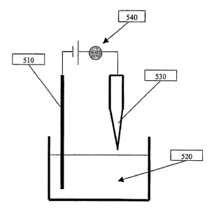
One such embodiment is illustrated in Figs. 5A-5B, where a dilute
suspension of nanotube or nanowire is first prepared. A counter electrode 510
is
first immersed into the suspension 520. The metal tip 530 is used as the
second
electrode. It is first placed perpendicular to the suspension surface with the
sharp
tip, where the nanotube/nanowire is to be deposited, just slightly above the
top
surface of the suspension. The tip is then gradually moved towards the surface
of
the suspension. A meter such as a current meter 540 is used to monitor the
electrical
l0 current between the counter electrode and the metal tip. In addition, an
appropriate
optical magnification device can be used to monitor the gap between the metal
tip
530 and the suspension surface 520. When the tip touches the surface of the
suspension, the electrical current passing between the two electrodes is
detected by
the meter 540. Depending on the concentration of the nanostructures in the
15 suspension and the electrical field used, the tip 530 is allowed to stay in
contact with
for a pre-determined time. The voltage applied between the two electrodes is
then
turned off and the tip 530 is raised to be above the suspension to stop the
deposition
process. The metal tip 530 with a carbon nanotube 550 or other nanostructure
attached to is vacuum annealed to increase the bonding between the tip and the
2o nanostructure. Figure 5C is an SEM image of a sharp tip having a single
nanotube
or nanowire deposited thereon according to the techniques of the present
invention.
Another application of the process of the present invention is fabrication of
triode-type structures with nanostructured field emission materials deposited
in
selected areas. Such structures can be used, for example, in field emission
flat panel
25 displays; cold cathodes for x-ray tubes, microwave amplifiers, etc.
In one embodiment of this application is illustrated in Figs. 6A-7B, where a
multilayer structure comprising a Si substrate 610, a dielectric insulating
layer 620
such as silicon dioxide, a conducting layer 630 and a layer of photoresist 640
is
fabricated by common thin film fabrication techniques (Fig. 6A). A photo-mask
is
30 used to selectively expose the photoresist 640 to ultraviolet light. The
multilayer
-18-
CA 02468685 2004-05-28
WO 03/075372 PCT/US02/37184
structure is then developed using suitable chemicals to remove the exposed
underlying multi-layer structure at the desired locations (Fig. 6B). As
illustrated in
Fig. 6B, the dimension D of the exposed areas of substrate 610 is small. For
example, D can be on the order of 1-100 micrometers, preferably 5-20
micrometers.
The exposed areas can be in the form of an array of rounded holes or polygons
such
as squares. As illustrated in Fig. 6C, carbon nanotubes or other
nanostructures are
selectively deposited on the exposed Si surfaces of substrate 610 by
electrophoresis.
In one embodiment, the chemical etched structure is immersed into a carbon
nanotube suspension. Contact to the power source is made on the back of
surface
610. A metal plate is used as the counter electrode. A bias voltage is also
preferably
applied to the conductive surface 630 to prevent deposition of carbon
nanotubes ~on
the metal surface. Under the applied electrical field, carbon nanotubes will
migrate
to the exposed surfaces of substrate 610.
For purposes of illustration, the dielectric layer 620 can have a thickness on
the order of 1-100 micrometers, preferably 1-10 micrometers.
Figure 7A and 7B show the top view of the etched mufti-layer structures
formed as described above.
In addition, the electrophoresis method of the present invention can also be
utilized to form a patterned deposit of nanostructure-containing material onto
a
2o substrate.
Figs. 8A to 8D illustrate one embodiment of this application. According to
the illustrated embodiment, a mask 640 is placed on top of a first surface of
a
substrate 650 before electrophoresis. The area 670 on the surface of substrate
650
where no deposition is intended is blocked by the mask 640, while the areas
660 on
the surface of substrate 650 are exposed to the electrophoresis bath through
corresponding openings in the mask 640.
The masked substrate is then introduced into a suspension and coated by
electrophoresis in a manner consistent with the present invention, as set
forth in
detail above.
After deposition, the mask 640 is removed from the substrate 650 and a clean
-19-
CA 02468685 2004-05-28
WO 03/075372 PCT/US02/37184
patterned structures 680 containing nanostructure-containing material is
obtained, as
illustrated in Fig. 8D. The dimensions) and shapes) of the patterned
structures are
defined by the openings of the mask 640.
Figures 8A and 8B show the side and the top view of the mask-blocked
substrate before electrophoresis. Figure 8C shows the side view of the mask-
blocked
substrate after electrophoresis. Figure 8D is the side view of the final
structures on
the substrate.
While the present invention has been described by reference to the above-
mentioned embodiments, certain modifications and variations will be evident to
to those of ordinary skill in the art. Therefore, the present invention is
limited only by
the scope and spirit of the appended claims.
-20-