Note: Descriptions are shown in the official language in which they were submitted.
CA 02468721 2004-05-28
WO 03/047692 PCT/GB02/05361
IMPROVEMENTS tN AND RELATING TO
PORTABLE DEFIBRILLATORS
This invention relates to portable defibrillators.
As is well known, a defibritlator is a therapeutic device used to treat
certain
cardiac irregularities such as ventricular fibrillation and pulse-less
ventricular
tachycardia where one or more high energy electrical pulses from a capacitor
bank are discharged into a patient via a pair of electrodes positioned on the
1 o patient's chest. Due to the complex waveform of such pulses and the need
to
deliver them at specific points in time following an assessment of the
patient's
condition, which may be done automatically by the defibrillator or manually,
it is
essential that the whole of the defibrillator circuitry is tested at regular
intervals
to guarantee that ~a lifesaving pulse may be given safely and effectively.
This
has traditionally been achieved by discharging the pulse across a load
resistor
of, typically, 50 ohms, in order to mimic the pulse which would otherwise be
discharged into a patient.
However, because the discharge of electrical energy is very high (anywhere up
2 0 to 360 Joules) and is delivered in a very short time (typically 5 to 20
milliseconds), the peak power requirement of the load resistor is quite
substantial, exceeding 72kW (360 Joules over 5 miiiiseconds). A consequence
of this is that during a discharge there is significant resistive heating of
the
discharge resistor such that it is customary to provide a heat sink around it,
which may take the form of an aluminium or copper sleeve incorporating heat
radiating fins.
CA 02468721 2004-05-28
WO 03/047692 PCT/GB02/05361
2
A further consequence of having such traditional self test methods is that the
physical size of the discharge resistor is relatively large and may use up a
substantial portion of the circuitry housing which, along with the traditional
use of
a heat sink, help to make the defibrillator bulky and heavy to handle, as well
as
being expensive to produce and maintain. This problem is exacerbated by the
fact that a full electrical discharge into the discharge resistor has a
correspondingly large drain on the battery power source and up to 400 Joules
per discharge are typically lost during a self test. This results in the
requirement
for a relatively large battery source, which further adds to the weight and
size
and hence detracts from the portability of the defibrillator.
The present invention is derived in part from the realisation that with the
use of a
processor to calculate projected characteristics of a pulse, even if
discharged
over a relatively long period, it is not necessary for the pulse to be
discharged
over such short periods during a self test in order for an accurate assessment
of
the ability of the defibrillator to deliver a lifesaving pulse when required.
Also, if
would be advantageous to provide a defibrillator which is relatively compact
and
lightweight, and may therefore be less expensive to produce and maintain.
2 0 In accordance with a first aspect of the invention there is provided a
portable
defibrillator which includes a processor and associated self test circuit in
which
during the self test electrical energy is discharged from one or a bank of
capacitors to a charge receiving circuit which recycles the energy back to a
rechargeable battery supply to thereby prolong the original charge within the
battery.
According to an alternative, second, aspect of the invention there is provided
a
CA 02468721 2004-05-28
WO 03/047692 PCT/GB02/05361
3
portable defibrillator which includes a processor and associated self test
circuit
in which during the self test electrical energy is discharged from one or a
bank of
capacitors to a charge receiving circuit containing a relatively high Ohmic
valuellow Waftage discharge resistor means (hereafter "high value resistor
means") such that the discharge occurs over a relatively long period of time
as
compared to traditional methods using a low Ohmic valuelhigh Wattage resistor
(hereafter "low value resistor") and associated heat sink. The high value
resistor
means may be a single high value resistor, but in a refinement to this concept
a
network of two or more smaller value resistors may be provided instead which
collectively provide a relatively high total resistance to the electric pulse
discharged by the defiibriilator during a self test.
As wilt be appreciated, the concepts of the fast and second aspects of the
invention may be incorporated into the same device with provision being made
in the circuitry permitting optional switching of the capacitor discharge
pulse so
that it is. either recycled directly back to a rechargeable battery supply, if
such is
present in the defibrillator, or is directed to the high value resistor means,
whether or not the defibrillator is powered by rechargeable batteries. This
switching may be carried out through the use of e.g. a micro-controller, but
could
also be by other means including a manually operated switch.
The recycling circuit option according to the first aspect of the invention is
chosen where rechargeable batteries are in use and energy needs to be
conserved because of self tests occurring when the batteries are not on
charge.
~5 Here, the swifiching circuit would direct the capacitor discharge pulse
during the
self test through a DC:DC conversion circuit and back to the battery.
Measurement of characteristics of the pulse during the self test could occur
CA 02468721 2004-05-28
WO 03/047692 PCT/GB02/05361
4
either at the capacitor end of the circuit by measuring the charge or voltage
drop
across one or more of fihe capacitors, or at the recycling stage.
The option of switching the capacitor discharge pulse to the high value
resistor
means can be used where battery energy need not or cannot be conserved,
such as where the batteries are non-rechargeable primary batteries, or if the
self test were occurring whilst rechargeable batteries were being charged from
some other source, such as a mains electricity supply, in this case, the
switching circuit would direct the capacitor discharge pulse from the
capacitors
1 o to the high value resistor means, whether it be a single high value
resistor or a
network of two or more smaller value resistors which collectively provide the
desired high Ohmic value/low Wattage resistance, during which measurement of
characteristics of the discharge pulse could be taken at either the capacitor
end
of the circuit by measuring the charge or voltage drop across one or more of
the
capacitors, or at the load stage i.e. across the high~value resistor means.
In a third aspect of the invention the self test is carried out on a bank'of
capacitors in rotation such that for one self test one capacitor is fully
charged
until a predetermined energy level is reached whilst the remaining capacitors
in
2 0 the bank are not, or may be only partially charged, and then following
discharge
during a self test, fihe next capacitor in the bank is fully charged for
discharge
during the next self test, the cycle repeating in sequence.
In a fourth aspect of the invention a single capacitor from a bank of
capacitors is
fully charged using the capacitor rotation described in the third aspect of
the
invention, but during the self test is discharged into the next capacitor, and
so
on, until all of the capacifiors in the capacitor bank have been charged and
CA 02468721 2004-05-28
WO 03/047692 PCT/GB02/05361
discharged, but only from substantially a single power input. Hence, if there
are
four capacitors in the capacitor bank the self test requires only 25%, before
capacitor leakage losses, of the energy that would otherwise be required for a
self test of the entire capacitor bank at the same time.
5
The invention wilt now be described, by way of example only, with reference to
the accompanying drawings in which:
Figure 1 is a schematic block diagram of defibrillator circuitry in accordance
with
- a first embodiment of the invention;
Figure 2 is a simplified circuit diagram of part of the circuitry of Figure 1;
Figure 3 is a schematic circuit diagram of second, third and fourth
embodiments
of the invention;
Figure 4 is a schematic circuit diagram of an alternative part of the circuit
diagram of Figure 3 in accordance with the second embodiment of the invention,
and;
~0
Figure 5 is a schematic circuit diagram showing in combination the various
embodiments of the invention.
Referring frrstly to Figure 1 there is shown a block diagram of a circuit for
use in
a portable defibrillator according to a first embodiment of the invention,
which
includes a rechargeable battery power source 1, a switch mode DC:DG
converter 2 which in one aspect converts low voltage current from the battery
1,
CA 02468721 2004-05-28
WO 03/047692 PCT/GB02/05361
6
typically 12 volts, to high voltage current to a charge control circuit 3,
typically
500 volts, which, in turn, is used to charge a capacitor bank 4 to a required
energy level for delivering e.g. an 80A pulse, in a manner to be described.
The
capacitor bank 4 is connected to an output switching circuit 5 which provides
for
a discharge from the capacitor bank 4 to be either fed to an automated
external
defibrillator (AED) connector 6 for discharging an electrical pulse to a
patient by
means of a pair of electrodes 7 if certain predetermined parameters are met,
or
instead to a recycle circuit 8 for recycling the pulse back to the battery 1
via the
DC:DC converter2 in a manner. to be described.
The defibrillator also includes a central processing unit 9 for receiving and
processing signals from an ECG monitoring circuit 10, as well as carrying out
other functions to be described. if the processor 9 recognises the ECG signal
to
be indicative of a shockable rhythm (such as Ventricular Fibrillation or
Ventricular Tachycardia for example) it instructs the charging circuit to
begin
charging the capacitor bank 4 from the output of the DC:DG converter 2. When
the correct charge level has been reached the processor 9 (whether
automatically or semi-automatically under command from the user) instructs the
output switching circuit 5 to discharge the pulse across the electrodes 7 in a
manner aimed e.g. to defibrillate a patient.
The processor 9 may also communicate the status of the patient to the
defibrillator user through indicators 17 or a loudspeaker 18. fn response, the
user can select and control the defbrillator device via the processor 9 by use
of
buttons 16, and a microphone 19 can be used to input an audio message to the
device for subsequent replay through the loudspeaker 'f 8. fn addition, the
processor 9 may also form part of a self test circuit for measuring and
monitoring
CA 02468721 2004-05-28
WO 03/047692 PCT/GB02/05361
7
electricat energy discharged from the capacitor bank 4, either within the
capacitor circuit or the recycle circuit, the circuit including the battery 1,
DC:DC
converter 2, charge control circuit 3, capacitor bank 4, output switching
circuit 5
and recycle circuit 8.
Turning now to Figure 2, there is shown a simplified circuit diagram. for
recharging the battery 1 following a self test and which forms part of the
recycle
circuit 8 shown in Figure 1, where tike parts are numbered the same. The
circuit
includes, in this embodiment, a bank of two capacitors 4 and a pair of
electrodes
7 for placing onto the chest of a patient prior to delivery of an electric
shock. In
this circuit switches 11,12 are shown closed for facilitating charging of the
capacitor bank 4 via a three-coil transformer 13, and are hence open against
delivering a charge from the capacitor bank 4. Switches 14,15 are shown closed
for returning a charge from the capacitor bank 4 when the switches 11,12 are
closed for delivering a charge from the capacitor bank 4. When this happens,
following a self test, the charge from the capacitor bank 4 is returned to the
transformer 13 and, via the DC:DC converter 2 which reduces the charge from,
typically, 2000 volts down to 12 volts, back to the battery 1.
0 As will be appreciated, when the switches 11,72 are closed for delivering a
pulse
of electricity from the capacitor bank 4, switches 14 and 15 can also be
closed
for delivering that pulse to the electrodes 7 and hence to a patient onto
which
they have been placed.
Hence, in this fiirst embodiment of the invention, it wilt be appreciated that
rather
than wasting the elecfirical discharge during a self test and therefore
incurring a
drain from the battery 1, it can be fed back infio the battery, so as to be
more
CA 02468721 2004-05-28
WO 03/047692 PCT/GB02/05361
8
efficient, thereby permitting smaller and/or fewer batteries to be used. For a
typical discharge the defibrillator discharge recycle circuit may provide up
to
50% of the pulse back to the rechargeable battery pack.
In Figure 3 there is shown part of a circuit diagram for a defibrillator
according to
a second, alternative, embodiment of the invention which in this case includes
a
bank 4 of four capacitors (C1, C2, C3 and C4) which are each activated by
controls from the processor 9 (not shown) via -a bank of respective field
effect
transistor (FET) switches 20 (F1, F2, F3 and F4). In this case the recycle
circuit
8 of Figures 1 and 2 has been replaced by an internal load in the form of high
value resistor means, being a single high value resistor 21 typically of
between
500K Ohm/10 Watts and 1 M Ohm/5 Watts rather than, as is conventionally the
case, the use of e.g. a 50 Ohml72 K Watt resistor which would otherwise be
- required for a self test discharge to test the integrity and viability of
the
l5 defibrillator components. In this case such may also include insulated gate
bipolar transistor (IGBT) switches (11, 12, 13 and 14) and silicon controlled
rectifier
(SCR) switches (S1, S2 and S3).
- As will be understood by those skilled in the art, by using such a high
value
resistor 21 the initial peak current during a self test discharge from the
capacitor
bank 4 is reduced to a fraction of ifs initial value as compared to the use of
a low
value resistor and hence the overall average power toss is also dramatically
decreased over time. During this period and/or afterwards, the processor 9 can
be used to calculate whether measured characteristics of the discharged pulse,
if given in a real-time lifesaving situation at the required power level, are
satisfactory for the purposes of the selfi test. A consequence of this is that
the
resistor 21 typically only has to handle e.g. 10 watts at 50010 Ohms or 5
watts at
CA 02468721 2004-05-28
WO 03/047692 PCT/GB02/05361
9
1 M Ohm with peak current values of 4mA and 2mA respectively from a typical
discharge pulse, such that the average discharge times across resistor 21 for
these values may be 16.5 minutes and 33 minutes respectively, ignoring
capacitor leakage losses.
Accordingly, by the use of a very high value resistor 21 it will be apparent
that
resistive heating is minimised such that the need for a heat sink, with its
attendant bulk and mass, is obviated, thereby making it possible to provide a
defiibril(ator which is relatively compact and lightweight.
In a refinement to the second embodiment of the invention two or more
resistors
can be used to reduce the power dissipated in each resistor, therefore
allowing
the use of smaller value resistors to provide the required high Ohmic
value/low
Wattage. An example of this is shown in Figure 4 where a bank of resistors 21a
(R1, R2, R3, R4, R5, R6, R7, R8 and R9) are shown replacing the single high
value resisfior 21 of Figure 3. In this example, each of the resistors would
only
receive one third of the current and voltage (i.e. one ninth the power) of a
typical "
self test discharge and hence would only receive 1 kW of power if the whole
network equalled a resistance of 50 Ohms, and only 1.1W if the network
2 0 resistance totalled 500K Ohms.
As wilt be appreciated, in order for the defibrillator to be capable of
discharging
energy over a relatively long period. of time, it cannot discharge internally
during
treatment of a patient but must instead retain its charge in case it is
required to
e.g. defibrillate. However, following treatment of a patient or during a self-
test
there is no necessity to dump the charge quickly, and indeed where there is a
bank of e.g. 4 capacitors, individual ones of such bank may be discharged
CA 02468721 2004-05-28
WO 03/047692 PCT/GB02/05361
I0
individually whilst others in the same bank may be kept fully charged.
The foregoing leads to the concepts of the third embodiment of the invention
which may also be illustrated by reference to Figure 3 where it will be seen
that
each of the capacitors (C1, C2, C3 and C4) may be charged independently from
the battery source via instructions from the processor 9 and the FET switches
(F1, F2, F3 and F4) on the switch bank 20. In this embodiment the energy
stored in each capacitor (C1, C2, C3, C4) is monitored by the processor 9 and
each is charged from the battery 1 until a predetermined energy level is
reached.
I O At this .point the processor 9 isolates the subject capacitor by
deactivating the
respective FET switch, and charges the next capacitor in the sequence.
In order to conserve energy the processor 9 may permit one capacitor to be
fully
charged prior to a selfi test while the others in the bank are only partially
charged
such that during the self test all capacitors in the capacitor bank 5 are
discharged into an internal load such as the high value resistor 21, or
alternatively, where the defibrillator is powered by a rechargeable battery,
to the
recycle circuit $ of Figure 1, such that various parameters of the discharge
pulse
can be monitored and measured during the test. For the next self test the next
2 0 capacitor in the bank can be fully charged and the others only partially
charged,
and so on, until all of the capacitors in the bank 4 have been tested at full
charge, whereafter the process repeats.
Capacitor rotation during successive self=tests therefore allows for extended
use
of the battery whilst still facilitating the testing of each of the capacitors
up to its
respective maximum value over.a required period of time. In addition,
reliability
of the self test is ensured because all of the capacitors in the capacitor
bank 4
CA 02468721 2004-05-28
WO 03/047692 PCT/GB02/05361
11
are tested in each self test. By utilising the concept of capacitor rotation
it has
been found that only approximately 60% ,of the energy~that would ordinarily be
required for a full self test on all of the capacitors in the capacitor bank 4
is
needed, whereas such a self test would ordinarily be undertaken simultaneously
on all capacitors in the bank.
In a fourth embodiment of the invention, which may again be illustrated by
reference to Figure 3, the switch bank 20 can be used to charge only one of
the
capacitors in the capacitor bank 4 at a time via instructions from the
processor 9.
1o During a self test, the charged capacitor can then be discharged into the
next
successive capacitor, which is then discharged into the next, and so on, until
all
of the capacitors have been charged and discharged from, essentially, a single
power input. By utilising capacitor rotation in this way, each capacitor can
nevertheless still be checked for full discharge capability over a period of
time
and, but for capacitor leakage losses, ~it will be appreciated that only 25%
of the
initial full self test energy is required, thereby prolonging the battery
and/or
permitting a smaller baftery to be used than would otherwise be the case.
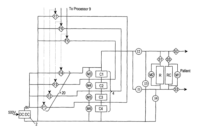
Turning now to Figure 5, this shows how the various embodiments of the
invention may be combined within or as part of a circuit to allow for e.g.
optional
switching between energy recycling during a self test as described with
reference to Figures 1 and 2, or energy discharge/dumping as described with
reference to Figures 3 and 4. In this circuit, where Like parts are again
numbered accordingly, the recycle circuit 8 is shown interposed in the circuit
adjacent to switches S2 and S3, being activated and deactivated by switch S5.
When activated, a measuring circuit M1 can be used to measure characteristics
of the electrical energy discharged from the bank of capacitors 4 prior to it
being
CA 02468721 2004-05-28
WO 03/047692 PCT/GB02/05361
I2
recycled to the rechargeable battery supply (not shown). Similarly, a
measuring
circuit MZ can be used to measure parameters of the electrical energy
discharged from the capacitor bank 4 during a self test through the high value
discharge resistor 21 when the switch S1 is open and the switch S5 is closed.
In order to measure the parameters of electrical energy discharged from each
of
the capacitors C1, C2, C3 and C4, respective measuring circuits M3, M4, M5
and M6 are interposed therebetween, although it will be appreciated that other
circuit configurations may be employed including, for example, the use of a
single measuring circuit across the whole bank of capacitors 4.
As will be apparent, a defibrillator incorporating the circuit of Figure 5
can, if
using rechargeable batteries, selectively benefit from the use of recycled
electrical energy through the recycling circuit 8 during a self test, thereby
prolonging the original charge within the battery and making it possible e.g.
to
utilise smaller or fewer batteries than would otherwise be the case. However,
irrespective of how the defibrillator is powered, ~rhether by primary cell,
rechargeable cell or mains electricity, the electrical energy can also be
discharged during a self test via the high value discharge resistor 21 over a
relatively long period of time, therefore obviafiing the need for a heat sink,
with its
attendant bulk and weight.
In all four embodiments of the invention, which may or may not be used
independently or in combination where feasible, whether partially or wholly,
it will
be understood that the objectives of the invention may be realised by the
provision of a defibrillator which is relatively small and lightweight as
compared
to conventional portable defibrillators, and may also be relatively
inexpensive to
CA 02468721 2004-05-28
WO 03/047692 PCT/GB02/05361
13
produce and maintain.