Note: Descriptions are shown in the official language in which they were submitted.
CA 02468789 2010-09-17
11581-2
SHAPED NANOCRYSTAL PARTICLES AND METHODS FOR MAKING THE SAME
BACKGROUND OF THE INVENTION
The ability to systematically manipulate the shapes of inorganic nanocrystal
particles remains a goal of modern materials chemistry. The shape and size of
inorganic nanocrystal particles control their widely varying electrical and
optical
properties. One means of achieving shape control is through the use of a
static
template to enhance the growth rate of one crystallographic face over another.
For
example, two-dimensional films are obtained when there is favorable epitaxy on
substrate (Cho, J. Cryst., Growth, 202:1-7 (1999)). Pyramidal "dots" are
obtained if
1o there is strain between the growing crystallite and the epitaxial
substrate, as in the
growth of InAs on GaAs (Leon et al., Science, 267:1966-1968 (1995)) and Ge on
Si
(Liu et al., Phys. Rev. Lett., 84:1958-1961 (2000)).
Anisotropic inorganic nanocrystal particles have also been grown in liquid
media. The vapor-liquid-solid growth mechanism in which a solid rod grows out
of a
supersaturated droplet has been used to create one-dimensional materials (Hu
et al.,
Accounts of Chemical Research, 32:435-445 (1999)), and has been applied to the
growth of (insoluble)
1
CA 02468789 2004-05-28
WO 03/054953 PCT/US02/37760
nanorods in a liquid medium (Trentler et al., Science, 270:1791-1794 (1995);
Holmes et al.,
Science, 287:1471-1473 (2000)).
[0005] While anisotropic nanocrystal particles are useful, it would be
desirable if
nanocrystal particles with other shapes could be formed. As will be explained
in further
detail below, complex shaped nanocrystal particles such as tetrapods have a
number of
features that make them more desirable than nanocrystal rods or spheres for
some
applications. Other advantages of complex shaped nanocrystal particles are
described below.
SUMMARY OF THE INVENTION
[0006] Embodiments of the invention are directed to shaped nanocrystal
particles and
methods for making shaped nanocrystal particles. The shaped nanocrystal
particles can be
branched (e.g., in the form of tetrapods), or can be in the form of teardrops
or arrows.
[0007] One embodiment of the invention is directed to a process of forming a
nanocrystal particle, the process comprising: (a) providing a core having a
first crystal
structure in a solution; and (b) forming an arm extending from the core having
a second
crystal structure in the solution, wherein the nanocrystal particle comprises
a Group IV
semiconductor, Group III-V semiconductor, a metal, a dielectric material, or a
Group II-VI
semiconductor including at least one Group II element and at least one Group
VI element
selected from the group consisting of 0, S, Te, and Po.
[0008] Another embodiment of the invention is directed to a process for
forming
semiconductor nanocrystal particles comprising: introducing semiconductor
nanocrystal
particle precursors into a mixture of surfactants capable of promoting the
growth of tetrapod
shaped semiconductor nanocrystal particles; and forming tetrapod shaped
semiconductor
nanocrystal particles, wherein each of the nanocrystal particles comprises a
Group IV
semiconductor, Group III-V semiconductor, a metal, a dielectric material, or a
Group II-VI
semiconductor including at least one Group II element and at least one Group
VI element
selected from the group consisting of 0, S, Te, and Po.
[0009] Another embodiment of the invention is directed to a nanocrystal
particle
comprising: a core having a first crystal structure; and at least an arin
extending from the core
having a second crystal structure, wherein the nanocrystal particle comprises
a Group IV
semiconductor, Group III-V semiconductor, a metal, a dielectric material, or a
Group II-VI
semiconductor including at least one Group II element and at least one Group
VI element
selected from the group consisting of 0, S, Te, and Po.
2
CA 02468789 2010-09-17
r K
11581-2
In one aspect, the present invention relates to a process of forming a
nanocrystal particle, the process comprising providing a core having a first
crystal
structure in a solution; and forming an arm extending from the core having a
second
crystal structure in the solution, wherein the nanocrystal particle comprises
CdTe.
In another aspect, the present invention relates to the process as described
herein, wherein the semiconductor nanocrystal particles have shapes comprising
branched tetrapod shapes.
In still another aspect, the present invention relates to the nanocrystal
particle
as described herein, wherein the arm is a first arm, and wherein the
nanocrystal
particle further comprises: at least a second arm extending from the core, the
second
arm having the second crystal structure; and at least a third arm extending
from the
core, the third arm having the second crystal structure.
In yet another aspect, the present invention relates to the branched
nanocrystal
particle as described herein, wherein the core has a diameter of about 3 nm to
about 4 nm, and wherein each of the first and second arms have a length from
about 4
nm to about 100 nm.
In a further aspect, the present invention relates to the tetrapod shaped
nanocrystal particle as described herein, wherein each of the first, second,
third, and
fourth arms has an aspect ratio greater than 1Ø
In yet a further aspect, the present invention relates to the photovoltaic
device
as described herein, wherein the arm is a first arm, and wherein the
nanocrystal
particle further comprises: at least a second arm extending from the core, the
second
arm having the second crystal structure; and at least a third arm extending
from the
core, the third arm having the second crystal structure.
In still a further aspect, the present invention relates to the photovoltaic
device
as described herein, further comprising second, third, and fourth arms
extending from
the core, wherein the nanocrystal particle is a tetrapod shaped nanocrystal
particle.
2a
CA 02468789 2004-05-28
WO 03/054953 PCT/US02/37760
[0010] Another embodiment of the invention is directed to a branched
nanocrystal
particle comprising: a core; at least a first arm extending from the core; and
at least a second
arm extending from the core, wherein the second arm forms a branch with
respect to the first
arm, and wherein the nanocrystal particle comprises a Group IV semiconductor,
Group III-V
semiconductor, a metal, a dielectric material, or a Group II-VI semiconductor
including at
least one Group II element and at least one Group VI element selected from the
group
consisting of 0, S, Te, and Po.
[0011] Another embodiment of the invention is directed to a tetrapod shaped
nanocrystal particle comprising: a core having a first crystal structure; a
first arm extending
from the core; a second arm extending from the core; a third arm extending
from the core;
and a fourth arm extending from the core, wherein the first, second, third,
and fourth arms
have a second crystal structure, wherein the first crystal structure is
different than the second
crystal structure, and wherein the nanocrystal particle comprises a Group IV
semiconductor,
Group III-V semiconductor, a metal, a dielectric material, or a Group II-VI
semiconductor
including at least one Group II element and at least one Group VI element
selected from the
Group consisting of 0, S, Te, and Po.
[0012] Another embodiment of the invention is directed to a nanocrystal
particle in
the form a teardrop or an arrow, wherein the nanocrystal particle comprises a
Group IV
semiconductor, Group III-V semiconductor, a metal, a dielectric material, or a
Group II-VI
semiconductor including at least one Group II element and at least one Group
VI element
selected from the Group consisting of 0, S, Te, and Po.
[0013] Another embodiment of the invention is directed to a process for
forming
shaped nanocrystal particles comprising: (a) mixing semiconductor precursors
and a mixture
of surfactants to form a solution; and (b) forming nanocrystal particles in
the solution,
wherein the nanocrystal particles are in the form of teardrops or arrows, and
wherein the
nanocrystal particles comprise a Group IV semiconductor, Group III-V
semiconductor, a
metal, a dielectric material, or a Group II-VI semiconductor including at
least one Group II
element and at least one Group VI element selected from the Group consisting
of 0, S, Te,
and Po.
[0014] Another embodiment of the invention is directed to a photovoltaic
device
comprising: a nanocrystal particle comprising a core having a first crystal
structure, and
at least an arm extending from the core having a second crystal structure.
3
CA 02468789 2004-05-28
WO 03/054953 PCT/US02/37760
[0015] Another embodiment of the invention is directed to a photovoltaic
device
comprising: a tetrapod shaped nanocrystal particle comprising, a core having a
first crystal
structure, a first arm extending from the core, a second arm extending from
the core, a third
arm extending from the core, and a fourth arm extending from the core, wherein
the first,
second, third, and fourth arms have a second crystal structure, and wherein
the first crystal
structure is different than the second crystal structure.
[0016] These acid other embodiments of the invention are described in further
detail
below.
BRIEF DESCRIPTION OF THE DRAWINGS
[0017] FIG. 1 shows a proposed model of a CdTe tetrapod.
[0018] FIG. 2(a) shows ensemble optical absorption spectra for a series of
tetrapods
having comparable arm lengths, but different diameters.
[0019] FIG. 2(b) shows ensemble optical absorption spectra for a series of
tetrapods
having comparable arm diameters, but different lengths.
[0020] FIG. 3(a) shows a schematic illustration of a tetrapod according to an
embodiment of the invention.
[0021] FIG. 3(b) shows a schematic illustration of a branched tetrapod
according to
an embodiment of the invention.
[0022] FIG. 3(c) shows a schematic illustration of an inorganic dendrimer
according
to an embodiment of the invention.
[0023] FIGS. 4(a)-4(c) show schematic 3-dimensional illustrations of how a
branched
tetrapod is formed.
[0024] FIG. 5 shows a transmission electron micrograph (TEM) of nanocrystal
particles made using 60% HPA in TOPO. Arrow-shaped nanocrystal particles are
shown.
[0025] FIGS. 6(a)-6(e) show transmission electron micrographs (TEMs) of
nanocrystal particles produced using 60 mole % HPA (FIG. 6(a)). High
resolution TEM
(HRTEM) images show the stages of growth from (FIG. 6(b)) pencil to (FIG.
6(c)) narrow
arrow to (FIG. 6(d)) pine-tree shaped nanocrystal particles. In FIG. 6(e), a
pine-tree shaped
nanocrystal is also shown looking down the [001] direction (or long axis).
HRTEM
characterization shows that each shape of nanocrystal is predominately
wurtzite, and that the
angled facets of the arrows are the (101) faces.
4
CA 02468789 2004-05-28
WO 03/054953 PCT/US02/37760
[0026] FIG. 7 shows a 2-dimensional representation showing the relationship
between
the wurtzite and zinc blende structures. Wurtzite has ABAB stacking while zinc
blende has
ABCABC stacking. The (111) face of zinc blende and the (001) face of wurtzite
both have
planes alternately composed of Cd and Se atoms. The two structures are related
by a stacking
fault.
[0027] FIGS. 8(a)-8(c) show transmission electron micrographs (TEMs) of (FIG.
8(a)) typical teardrop shaped nanocrystal particles. A high resolution TEM
(HRTEM) image
(FIG. 8(b)) shows the wurtzite structure of particles that are teardrop
shaped. FIG. 8(c)
shows a HRTEM image of a nanocrystal, which after an additional injection
shows growth on
both the (001) and (001) faces. The center of this particle is zinc blende in
structure.
[0028] FIGS. 9(a)-9(b) show high resolution transmission electron microscope
(HRTEM) images of tetrapod nanocrystal particles. FIG. 9(a) shows a typical
tetrapod
shaped CdSe nanocrystal particle, looking down the [001] direction of one arm.
Lattice
spacings confirm that all four arms are of the wurtzite structure. FIG. 9(b)
shows a tetrapod
that has branches growing out of each ann. There are zinc blende layers near
the ends of the
original arms and the branches are wurtzite with some stacking faults.
[0029] FIG. 10 shows an atomic model of CdSe in the wurtzite structure
demonstrating the differences between the (001) and (001) faces. On the (001)
face, Cd
atoms have only one dangling bond, while on the (001) face, Cd atoms have
three dangling
bonds that need to be passivated.
[0030] FIG. 11 shows a 2-dimensional representation showing the structure of a
tetrapod. The nuclei is the zinc blende structure, with wurtzite arms growing
out of each of
the four (111) equivalent faces. Three are shown, with the fourth coming out
of the page
towards the reader.
[0031] FIG. 12 shows transmission electron micrographs (TEMs) of CdTe
tetrapods
grown under various reaction conditions.
[0032] FIG. 13 shows TEMs of CdTe tetrapods extracted from the same synthesis
at 1
and at 5 minutes, respectively, for two syntheses carried out at the same
Cd/Te ratio (5:1), but
at two different Cd/ODPA ratios (1:2 and 1:5).
[0033] FIG. 14 shows a typical powder X-ray diffraction (XRD) of a CdTe
tetrapod
sample (non-vertical line with peaks). The bulk XRD pattern of CdTe wurtzite
is also shown
(vertical lines).
5
CA 02468789 2004-05-28
WO 03/054953 PCT/US02/37760
DETAILED DESCRIPTION
[0034] In embodiments of the invention, the shapes of colloidal semiconductor
nanocrystal particles can be systematically varied using the thermal
decomposition of
organometallic precursors in a hot mixture of surfactants. The hot mixture of
surfactants may
comprise, for example, trioctylphosphine oxide (TOPO) and an alkylphosphonic
acid. As in
the growth of spherical CdSe nanocrystal particles in hot trioctylphosphine
oxide, the
surfactants dynamically adsorb to the growing crystallites, allowing atoms to
add and subtract
for high crystallinity. This enables the growing crystallites to anneal,
resulting in good
crystallinity, while suppressing particle aggregation.
[0035] Controlled nanocrystal particle growth can depend on a number of
factors.
For example, the growth mode of the nanocrystal particles can be controlled by
adjusting the
monomer concentration. At low monomer concentration, Ostwald ripening occurs,
and small
nanocrystal particles can dissolve at the expense of larger ones. Such slow
growth conditions
favor the fonnation of a spherical particle shape (i.e., the nanocrystal
particles want to form
in a way that minimizes surface area). On the other hand, at high monomer
concentration,
relative differences between the growth rates of different faces can lead to
anisotropic shapes.
Using control mechanisms such as this, the present inventors herein
demonstrate surprisingly
the controlled formation of nanocrystal particles with tetrapod, teardrop, and
arrow shapes.
[0036] As used herein, "nanocrystal particles" can refer to crystalline
particles that
have at least one dimension less than about 100 nanometers. In some
embodiments of the
invention, the nanocrystal particles may have two or more dimensions that are
less than about
100 manometers. For example, the branched nanocrystal particles according to
some
embodiments of the invention can have arms that have aspect ratios greater
than about 1. In
other embodiments, the arms can have aspect ratios greater than about 5, and
in some cases,
greater than about 10, etc. The widths of the arms may be less than about 200,
100, and even
50 nanometers in some embodiments. For instance, in an exemplary tetrapod with
a core and
four arms, the core can have a diameter from about 3 to about 4 nanometers,
and each arm
can have a length of from about 4 to about 50, 100, 200, 500, and even greater
than about
1000 nanometers. Of course, the tetrapods and other nanocrystal particles
described herein
can have other suitable dimensions. In embodiments of the invention, the
nanocrystal
particles may be single crystalline or polycrystalline in nature.
[0037] The nanocrystal particles according to embodiments of the invention can
have
unique optical, electrical, magnetic, catalytic, and mechanical properties,
and can be used in a
6
CA 02468789 2004-05-28
WO 03/054953 PCT/US02/37760
number of suitable end applications. They can be used, for example, as fillers
in composite
materials, as catalysts, as functional elements in optical devices, as
functional elements in
photovoltaic devices (e.g., solar cells), as functional elements in electrical
devices, etc.
[0038] I. Branched nanocrystal particles
[0039] Snowflakes are a familiar example in which a solid is formed with a
high
degree of branching. The branching of snow crystals is due to growth far from
equilibrium,
at high supersaturation levels of water. Higher levels of complexity arise
when the growing
snow crystals experience regions of different temperature and partial pressure
of water as
they fall, changing the relative growth rates of the different
crystallographic facets.
[0040] Like snowflakes, embodiments of the invention can exhibit polytypism,
or the
existence of two or more crystal structures in different domains of the same
crystal.
Polytypism can be exploited to produce branched inorganic nanostructures in a
controlled
way. Frequently, polytypic structures share a common crystal facet, which is
desirable for
branching. In conventional macroscopic inorganic crystal growth, there are few
examples of
the controlled formation and growth of polytypic structures. There are also
few examples of
modulating growth rates of different crystal facets of a solid as a function
of time. However,
new methods for preparing inorganic nanocrystal particles with well-controlled
sizes and
shapes (e.g., spheres, rods, disks, and cubes) provide tools that can be
adapted to form unique
nanocrystal particles.
[0041] The tools can be used during the formation of nanocrystal particles to
promote
the stability of a certain phase over another and hence the formation of one
crystal phase over
another. This creates a new opportunity to generate artificial inorganic
nanostructures with
deliberately designed branches and interconnections.
[0042] Polytypism is generally prevalent in open, tetrahedrally bonded
structures such
as those occurring in the Group IV, III-V and II-VI semiconductors. In those
semiconductors, there is only one type of chemical bond with local tetrahedral
geometry.
The tetrahedral building blocks are arranged in puckered rings, are comprised
either of all
chairs (cubic or zinc blende case) or are mixtures of chairs and boats
(hexagonal or wurtzite
case). The cubic and hexagonal structures differ only by their second nearest
neighbor. The
{111} facets of the cubic crystal of these materials are atomically identical
to the (0001)
facets of the hexagonal structure. These identical facets allow a nanocrystal
particle to start
7
CA 02468789 2004-05-28
WO 03/054953 PCT/US02/37760
growing with one type of crystal structure (e.g., a cubic crystal structure)
and then transition
to form a second type of crystal structure (e.g., a hexagonal crystal
structure).
[0043] While the nanocrystal particles of embodiments of the invention can
have any
suitable material, CdTe is a particularly suitable candidate material for
controlled branching.
This is because this material has an appropriate energy difference between
zinc blende and
wurtzite structures. The energy difference between zinc blende and wurtzite in
the bulk can
be larger than 10 meV per atom for the most covalently or the most ionic
structures (such as
Si, GaAs, or ZnO), which rarely show polytypism. In contrast, moderately ionic
structures,
such as CdS and ZnS, occur almost indiscriminately in both phases due to an
energy
difference of only a few meV. In CdTe, this value is about 7 meV/atom,
offering the
possibility to control polytypism more easily. In CdTe, the cubic crystal
structure is
intrinsically more stable than the hexagonal crystal structure at the
temperatures in which
they can be grown in organic solution. Nucleation occurs in the cubic crystal
phase, even
though processing conditions may favor the growth of a hexagonal crystal
structure. In
embodiments of the invention, the energy difference between different crystal
structures in a
particular material is preferably less than 20meV/atom, less than 15meV/atom,
or less than 10
meV/atom so that polytypic structures can be created.
[0044] For CdTe and other materials, if the growth of the nanocrystal particle
takes
place at high temperatures (e.g., greater than about 290 C for CdTe) and/or
at a suitably high
monomer concentration and/or in the presence of a surfactant that promotes it,
then the
growth of a hexagonal wurtzite structure can be favored over a cubic zinc
blende structure.
(It is understood that the processing temperatures may vary depending upon the
particular
material produced.) These surfactant molecules are known to selectively
stabilize the facets
perpendicular to the c-axis of hexagonal nanocrystal particles. This
stabilization considerably
reduces the growth rate of these facets, which have no equivalent in the cubic
structure.
Thus, in the presence of phosphonic acid, nanocrystal particles such as CdTe
nanocrystal
particles nucleate zinc blende and grow in the wurtzite phase. Here, the
present inventors
demonstrate the reproducible synthesis, in high yield, of tetrapod shaped
nanocrystal particles
based upon this scheme.
[0045] In some embodiments, processing conditions can be adjusted or selected
to
allow for the formation of nanocrystal particles such as tetrapods, bipods,
tripods, branched
tetrapods, and inorganic dendrimers. Processing conditions can be adjusted or
selected to
favor the growth of one crystal structure over another to grow cores or arms
as desired. For
example, for compound semiconductors such as CdSe and CdTe, low reaction
temperatures
8
CA 02468789 2004-05-28
WO 03/054953 PCT/US02/37760
favor the formation of a cubic crystal structure, while higher reaction
temperatures favor the
formation of a hexagonal crystal structure. Low monomer concentrations favor
the formation
of a cubic crystal structure, while high monomer concentrations favor the
formation of a
hexagonal crystal structure. Parameters such as these can be manipulated to
favor the growth
of one crystal structure over another. For example, processing conditions can
be selected so
that they are favorable to the formation of a cubic crystal core structure.
Then, they can be
adjusted so that they are favorable to the formation of hexagonal crystal arm
structures. As
will be explained in detail below, using such methods, polytypic nanocrystal
particles can be
formed.
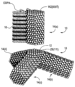
[0046] A tetrapod shaped nanocrystal particle 10 according to an embodiment of
the
invention is shown in FIG. 1 and has a zinc blende core 12 with four ::L {1 11
} facets 18, each
projecting a wurtzite arm 14(a), 14(b), 14(c), 14(d) that is terminated with
the ( 0001 )
facet 16. In FIG. 1, the exploded view of one arm 14(a) illustrates the
identical nature of the
(111) zinc blende (ZB) and (0001 ) wurtzite (WZ) facets of the core and the
arms,
respectively. Phosphonic acid molecules 16 selectively bind to the lateral
facets of the arms
14(a)-14(d), as suggested in the figure (for clarity, only two facets are
shown covered) to
inhibit growth on these facets. High-resolution TEM analysis would further
clarify the shape
of the cubic nucleus and the relative orientations between the various arms of
the tetrapod.
[0047] Although CdSe and CdTe branched nanocrystal particles are described in
detail herein, the branched nanocrystal particles may comprise any material.
For example,
the particles may comprise semiconductors such as compound semiconductors.
Suitable
compound semiconductors include Group II-VI semiconducting compounds such as
MgS,
MgSe, MgTe, CaS, CaSe, CaTe, SrS, SrSe, SrTe, BaS, BaSe, BaTe, ZnS, ZnSe,
ZnTe, CdS,
CdSe, CdTe, HgS, HgSe, and HgTe. Other suitable compound semiconductors
include
Group III-V semiconductors such as GaAs, GaP, GaAs-P, GaSb, InAs, InP, InSb,
AlAs, Alp,
and AlSb. The use of Group IV semiconductors such as germanium or silicon may
also be
feasible under certain conditions. In other embodiments, the particles may
comprise a
dielectric material such as SiC, SiN or any other material that can exhibit
polytypism. Some
metals such as Fe, Ni, Cu, Ag, Au, Pd, Pt, Co and others may also exhibit
polytypism and can
be used in embodiments of the invention.
9
CA 02468789 2010-09-17
11581-2
A. Methods For Forming Branched Nanocrystal Particles
Embodiments of the invention include methods of forming branched,
nanocrystal particles. In one embodiment, the method comprises forming a core
having a first crystal structure in a solution. The core may have a cubic
crystal
structure (e.g., a zinc blende structure) or any other suitable crystal
structure. Then,
one or more arms can form from the core, simultaneously or sequentially. The
arms
may have different crystal structures than the core. If a tetrapod is formed,
the
tetrapod may have first, second, third, and fourth arms, each with a hexagonal
crystal
structure extending from the core.
The types of precursors used to form the branched, nanocrystal particles
depend on the particular nanocrystal particles to be formed. In some
embodiments,
the precursors used to synthesize the nanocrystal particles include Group II,
III, Iv, V,
and/or VI semiconductor precursors. For example, in embodiments of the
invention,
semiconductor nanocrystal particles including a Group II-VI compound
semiconductor
can be the reaction product of at least one precursor containing a Group II
metal
containing precursor and at least one precursor containing a Group VI element,
or a
precursor containing both a Group II and a Group IV element. In other
embodiments of
the invention, semiconductor nanocrystal particles including a Group III-V
compound
semiconductor can be the reaction product of at least one precursor containing
a
Group III element and at least one precursor containing a Group V element, or
a
precursor containing both a Group III and a Group V element. Other exemplary
precursors, surfactants, and solvents can be found in U.S. Patent Nos.
6,225,198
and 6,306,736.
If Group III-V semiconductor nanocrystal particles are to be synthesized, a
Group III precursor, such as elemental Ga, In, Al, or any compound containing
a
Group III precursor, such as a Galll salt, InIIl salt, or AIIII salt (e.g., of
a halide, or
corresponding metal-carbon trialkyls) can be reacted directly with an arsenic,
phosphorus, or antimony source such as arsine, phosphine, or stibine; an alkyl
arsine,
phosphine or stibine; or an alkyl silyl arsine, phosphine or stibine in liquid
phase at an
3o elevated temperature. Representative metal sources include GaCl3, GaBr3,
InCI3,
CA 02468789 2010-09-17
11581-2
AIC13, Ga(ME)3, Ga(Bu)3, or the like. Representative arsenic, phosphorus and
selenium sources include AsH3, PH3, SeH3, AsH2 (carbon alkyl), As(carbon
alkyl)3,
P(carbon alkyl)3, As(Si(carbon alkyl)3)3, P(Si(carbon alkyl)3)3, Se(Si(carbon
alkyl)3)3
and the like. Although specific examples of precursors are
10a
CA 02468789 2004-05-28
WO 03/054953 PCT/US02/37760
provided, any Group III or V element and any compound containing such an
element can be
used in embodiments of the invention.
[0052] If Group II-VI semiconductor nanocrystal particles are to be
synthesized, they
may be the product of a reaction containing at least one precursor comprising
a Group II
element such as Zn, Cd, or Hg, or any Group II containing molecule such as a
metal, salt,
oxide, organometallic compound, and at least one precursor comprising a Group
VI element
such as 0, S, Se, or Te, or any Group VI containing molecule such as- a metal,
salt, oxide,
organometallic compound, or a precursor containing both a Group II element
(Zn, Cd, or Hg)
and a Group VI element (S, Se, or Te). Those of skill in the art can select
the appropriate
precursors to form the appropriate compound semiconductor. For example,
Cd(CH3) and
Se:TOP are examples of precursors respectively containing Group II and Group
VI elements
that can be used to forin CdSe nanocrystal particles.
[0053] The precursors may be dissolved in any liquid compatible with the
surfactant
mixture. Examples of organic liquids include polar organic solvents including
trialkyl
phosphine, e.g., tributyl phosphine. In some embodiments, the precursors maybe
dissolved
in the same solvent or may be dissolved separately to form two or more
precursor solutions.
[0054] Embodiments of the invention can use a surfactant mixture to make the
semiconductor nanocrystal particles. The surfactant mixture can be a high
boiling point
liquid mixture of two or more reactive or non-reactive organic surfactants.
The mixture of
these organic surfactants is capable of promoting the growth of branched
semiconductor
nanocrystal particles.
[0055] The surfactant mixture can have a boiling point that is high enough so
that a
reaction between, for example, the Group II and Group VI precursors, or the
Group III and
Group V precursors, can take place to form the desired semiconductor
nanocrystal particles.
For example, in some embodiments, the surfactant mixture can have a boiling
point between
about 200 C to about 400 C.
[0056] The surfactant mixture may include any suitable number of different
surfactants. For example, the surfactant mixture may include a first organic
surfactant and a
second organic surfactant. Third, fourth, fifth, etc. surfactants could also
be used. For
example, in some embodiments of the invention, at least one or two of the
surfactants can be
selected from the group consisting of a phosphonic acid, trioctylphosphine
oxide, an amine,
oleaic acid, and stearic acid. As noted above, the surfactant mixture can be
capable of being
heated to a crystal-growing temperature, and can promote the growth of
branched
semiconductor nanocrystal particles such as tetrapods.
11
CA 02468789 2004-05-28
WO 03/054953 PCT/US02/37760
[0057] The first surfactant in the surfactant mixture may comprise a
phosphorus-containing surfactant capable of withstanding such crystal-growing
temperatures.
Examples of such first phosphorus-containing liquid surfactants include liquid
surfactants
such as 3-30 (or larger) carbon trialkyl phosphines (e.g., tributyl
phosphine), or 3-30 or larger
carbon trialkyl phosphine oxides (e.g., trioctyl phosphine oxide or "TOPO").
The first
surfactant may also include other surfactants including molecules including
functional groups
such as amines; carboxylic acids, and any other groups as long as they are
stable.
[0058] The surfactant mixture can include a second organic surfactant. The
second
organic surfactant may be capable of being heated to crystal-growing
temperatures and may
be capable of promoting the growth of branched semiconductor nanocrystal
particles.
Preferably, the second liquid surfactant capable of promoting the growth of
branched
semiconductor nanocrystal particles can comprise a phosphorus-containing
surfactant capable
of withstanding such crystal-growing temperatures.
[0059] The second organic surfactant may comprise an organic-substituted acid,
or
acid salt surfactant containing phosphorus such as, for example, phosphonic
and phosphinic
acids. Suitable phosphinic acids may include mono and diphosphinic acids
having the
general formula R'R,,H(l.. )POOH, where R and R' are the same or different 3-
30 carbon (but
preferably 3-30 carbon) organic groups such as alkyl or aryl groups, and x is
0-1. In some
embodiments, the second organic surfactant comprises a 3-30 carbon alkyl
phosphonic acid,
e.g., octadecyl phosphonic acid.
[0060] The second organic surfactant is preferably a long chain length
phosphonic
acid. Short chain length phosphoric acids are defined as those having an alkyl
chain length
of less than or equal to about 10 carbon atoms. Long chain length phosphonic
acids are
defined as those having an alkyl chain length of greater than or equal to
about 10 carbon
atoms. In preferred embodiments, the phosphonic acid is at least 14 carbon
atoms long. An
example is octyldecylphosphonic acid (ODPA). For materials such as CdTe, these
long chain
length phosphonic acids help to promote the growth of hexagonal crystals.
[0061] In embodiments of the invention, a solution of one or more precursors
can be
slowly and/or quickly injected into a heated surfactant mixture. Injecting
precursors slowly is
a relative term that is readily determinable by one having ordinary skill in
the art. It can
include adding precursors drop by drop or no faster than 10 drops/sec, 5
drops/sec, 2 drops/
sec, or 1 drop/sec. Injecting precursors quickly is also a relative term
readily determinable by
one having ordinary skill in the art. It can include adding precursors at a
speed greater than
12
CA 02468789 2004-05-28
WO 03/054953 PCT/US02/37760
100 drops/sec, 20 drops/sec, or 10 drops/sec. For example, injecting
precursors quickly can
include emptying a 5 mL syringe holding the precursor as quickly as possible.
[0062] A solution of precursors can be injected into the surfactant mixture at
a cold or
low temperature solution so that immediately after the injection, the
temperature of the hot
mixture of surfactants drops to a second, lower temperature. Initially, the
heated surfactant
mixture may or may not contain other precursors. A pipette or a pressure
nozzle may be used
as an injection apparatus. The temperature can be kept constant during the
nanocrystal
growth. The resulting mixture is maintained at a first temperature, which
results in the
nucleation of seed crystals.
[0063] It is understood that the different precursors could be in their own
separate
solutions and these different solutions could be separately injected into the
heated surfactant
mixture in embodiments of the invention. For example, if CdSe nanocrystal
particles are to
be formed, a Cd precursor solution and a Se precursor solution can be
separately and
sequentially injected into a hot surfactant mixture to produce branched CdSe
nanocrystal
particles. The separate injection of precursors into a hot surfactant mixture
is preferred as it
results in better control of the reaction, which can allow a higher percentage
of branched
nanocrystal particles if desired (e.g., a higher percentage of tetrapods).
[0064] The precise reaction time may vary depending on the particular material
used
and the particular type of nanocrystal particles formed. In some embodiments,
a 5 minute
reaction time may be sufficient, while less than or more than 5 minutes may be
desirable in
other embodiments.
[0065] Subsequent nanocrystal growth can then stopped by a further reduction
of the
temperature to below the temperature at which nanocrystal growth occurs.
Cessation of the
crystal growth may be accomplished by rapidly reducing the temperature to
ambient
temperature or even lower, e.g., to less than 150, 100, 75, 50, or 25 C or
lower, e.g., by
removing the heating mantle that was used as a heat source. The temperature
can be reduced
more rapidly if the solution is cooled with a stream of air, cold water,
liquid nitrogen, dry ice
or other cooling agent.
[0066] After they are formed, the semiconductor nanocrystal particles can be
separated from the liquid medium that is used to form them. In some
embodiments, a solvent
such as methanol or acetone is added to the liquid medium containing the
semiconductor
nanocrystal particles to precipitate them. For example, CdSe particles are
generally not
soluble in polar solvents such as methanol or acetone. Any appropriate solvent
can be added
to precipitate the nanocrystal particles from the solution.
13
CA 02468789 2004-05-28
WO 03/054953 PCT/US02/37760
[0067] After the nanocrystal particles have precipitated, the precipitated
nanocrystal
particles are separated from the rest of the solution. In some embodiments,
centrifuging can
be used to separate the nanocrystal particles from other solution components.
After
centrifuging, the supernatant can be separated from the nanocrystal particles.
The
nanocrystal particles can then be stored as precipitate or can be dried in a
vacuum.
[0068] In a typical synthesis of CdTe tetrapods, a mixture of
octadecylphosphonic
acid (ODPA), trioctylphosphine oxide (TOPO) and cadmium oxide (CdO) is
degassed at-
120 C for 20 minutes and is slowly heated under Ar until the CdO decomposes
and the
solution turns clear and colorless. Next, 1.5 g of trioctyl phosphine (TOP) is
added, and the
temperature is further raised to 320 T. After that, Te:TOP (concentration of
Te 10 % by
weight) is quickly injected into the solution. The temperature drops to 315 C
and is
maintained at this value throughout the 5 minute synthesis. The resulting
tetrapods are
obtained in high yield, and they are soluble in common organic solvents, such
as toluene and
chloroform.
[0069] In some embodiments, branched nanocrystal particles such as tetrapods
may
be co-formed with other types of nanocrystal particles such as rods or
spheres. If this occurs,
it is possible to separate the tetrapods from the rods to increase the
percentage of tetrapods in
a given sample. For example, a solution may contain nanocrystal rods and
tetrapods. The
tetrapods can constitute more than about 1%, 5%, 10%, 20%, 40%, 60%, 80%, 90%,
95%, or
99% of all particles in the initial sample depending on the growth conditions.
Processes for
separating tetrapods from other nanocrystals are described in the Examples
below.
[0070] Because the branched nanocrystal particles according to embodiments of
the
invention can be formed in a surfactant mixture, the nanocrystal particles
that result may be
functionalized with surfactant molecules. For example, the core, and/or arms
of a nanocrystal
particle according to embodiments of the invention may be functionalized with
any of the
above-mentioned surfactant molecules (e.g., amphiphilic molecules). It is
noted that the
arrow and teardrop shaped nanocrystal particles described below could also be
functionalized
with surfactant molecules.
[0071] The branched nanocrystal particles according to embodiments of the
invention
can be formed with arms of any suitable length or diameter. It is possible to
control the phase
during nucleation and growth, and to manipulate the growth kinetics of the
nanocrystal
particles to enable independent tuning of the arm lengths and diameters. The
present
inventors have found that once the basic tetrapod shape is formed, growth of
the arms occurs
14
CA 02468789 2004-05-28
WO 03/054953 PCT/US02/37760
according to the controllable kinetic mechanisms previously observed for
nanorods. See, for
example, Manna et al., J. Am. Chem. Soc. 2000, 122, 12700-12706.
[0072] For example, with respect to CdTe tetrapods, higher Cd/Te ratios result
in
longer arms, while more phosphonic acid per Cd yields larger arm diameters.
Anisotropy
results from fast growth, and the growth rate is limited by the concentration
of the Cd
precursor, which is a strong complex between Cd2+ and phosphonic acid. Hence,
higher
Cd/Te ratios keep the reaction in the anisotropic growth regime longer,
leading to- longer
arms. On the other hand, the presence of more phosphonic acid per Cd (lower
Cd/ODPA
ratio) likely decreases the diffusion constant of the Cd precursor and the
driving force for its
addition to the crystal, thereby slowing the growth rate for a given Cd
concentration.
However, the growth of the arms continues as long as Cd concentration is
sufficiently high.
This results in less anisotropic rods, with a larger diameter for a given
length.
[0073] Tetrapods with arms of identical length can also be formed. This
generally
involves the simultaneous development of the four wurtzite arms and a highly
homogeneous
environment around the growing tetrapod structure. This implies, for instance,
a fast and
isotropic supply of monomer species from the bulk. When these homogenous
conditions are
not present, some arms can grow substantially slower than others, or even not
at all, resulting
in so-called "tripods", "bipods" and "monopods". Tripods and bipods are
examples of
branched nanocrystal particles. Additionally, missing arms can be due to
differences in the
shrinkage rate of the various arms in the same tetrapod.
[0074] The nanocrystal particles according to embodiments of the invention can
have
a variety of interesting mechanical, electrical, and optical properties. For
example, due to
their three dimensional character, tetrapods may be important alternatives to
nanocrystal
fibers and rods as additives for mechanical reinforcement of polymers (e.g.,
polymeric
binders including polyethylene, polypropylene, epoxy functional resins, etc.).
Tetrapod
shaped nanocrystal particles, for example, can interlock with each other and
can serve as a
better reinforcing filler in a composite material (e.g., with a binder), than
for example,
nanospheres. The nanocrystal particles can be mixed with the binder using any
suitable
mixing apparatus. After the composite material is formed, the composite
material can be
coated on a substrate, shaped, or further processed in any suitable manner.
[0075] The nanocrystal particles according to embodiments of the invention can
also
have unique optical properties. For example, FIGS. 2(a) and 2(b) compare the
electronic
absorption spectra for two series of tetrapod samples having different arm
lengths and
diameters. In a tetrapod shaped nanocrystal, most of the confinement energy is
along the
CA 02468789 2004-05-28
WO 03/054953 PCT/US02/37760
diameter of the hexagonal arms. Tetrapods having comparable arm lengths but
different
diameters, show remarkable differences in their band gap energy (FIG. 2(a)).
While spectra
of tetrapods with comparable diameters but different arm lengths, are almost
identical (FIG.
2(b)). This independent tunability of the arm length and the band gap is very
attractive for
nanocrystal based solar cells or other types of photovoltaic devices.
Exemplary photovoltaic
devices are described in, for example, Science, Vol. 295, pp. 2425-2427, March
29, 2002. An
exemplary photovoltaic device may have nanocrystal particles in a binder: This
combination
can then be sandwiched between two electrodes (e.g., an aluminum electrode and
an indium
tin oxide electrode) on a substrate to form a photovoltaic device.
[0076] The inherent property of a tetrapod to self-align on a substrate with
one arm
always pointing towards one electrode, combined with the low band gap material
such as
CdTe, should substantially enhance the device efficiencies of recently
reported hybrid
nanorod-polymer solar cells. In comparison to nanocrystal particles that are
randomly
oriented, the tetrapods according to embodiments of the invention are aligned
and can
provide for a more unidirectional current path than randomly oriented
nanocrystal particles.
[0077] Although tetrapods have just been described in detail, it is understood
that
embodiments of the invention include even more complex shaped nanocrystal
particles. In
embodiments of the invention, the initial nucleation event yields a core with
a cubic crystal
structure (e.g., a zinc blende crystal structure). Later, arms with a
hexagonal crystal structure
(e.g., wurtzite) can grow out from the core. However, different growth
conditions can be
provided to statistically alternate the formation of cubic and hexagonal
crystal structures, thus
leading to irregular branching. Precise control of temperatures throughout the
reaction may
yield sequentially branched "inorganic dendrimers". This can be illustrated
with reference to
FIGS. 3(a)-3(c).
[0078] FIG. 3(a) shows a tetrapod 300 according to an embodiment of the
invention
looking down one arm of the tetrapod 300. The tetrapod 300 includes a cubic
core 102(a)
and four arms with hexagonal crystal structures extending from the cubic core
102(a).
Adjacent arms can form angles of about 109.5 degrees (it has tetrahedral
symmetry) in some
embodiments. In FIG. 3(a), three arms 104(a)-104(c) are shown, with the fourth
arm of the
tetrapod extending toward the reader. As shown, each arm can include a
proximate end and a
distal end. For example, the arm 104(a) has an end 104(a)-i that is proximate
to the core
102(a) and an end 104(a)-2 that is distal to the core 102(a).
[0079] In the formation of the tetrapod, the cubic core 102(a) forms and then
the
four arms having a hexagonal crystal structure grow from that core 102(a).
Processing
16
CA 02468789 2004-05-28
WO 03/054953 PCT/US02/37760
conditions can be adjusted to cause the arms to grow from the core 102(a) or
the arms may
inherently form from a given set of conditions. For example, for CdTe
nanocrystal particles,
providing hexagonal crystal growing conditions can result in tetrapods without
the need to
adjust processing conditions. As the present inventors have demonstrated,
simply providing
conditions favorable hexagonal crystal growth can result in CdTe tetrapods.
Alternatively, as
shown in the CdSe tetrapod examples below, processing conditions can be
adjusted to form
branches. Higher monomer concentrations (e.g., adding more precursor to a
surfactant
mixture) and higher temperatures can be used to induce the formation of arms
with hexagonal
crystal structures, while lower monomer concentrations and lower temperatures
can be used
to induce the formation of cubic crystal structures.
[0080] With this in mind and referring to FIG. 3(b), once the basic tetrapod
is formed,
additional branches on the tetrapod can be formed. For example, as shown in
FIG. 3(b),
additional arms 106(a), 106(b) can form from a second core 102(b) at the
distal end 104(a)-2
of the arm 104(a). The arms 106(a), 106(b) may appear as branches. As a
result, another
tetrapod can form at the distal end 104(a)-2 of the arm 104(a). The resulting
nanocrystal
particle may be a branched tetrapod 301.
[0081] To form the branched tetrapod 301 in FIG. 3(b), an initial tetrapod 300
can
first be formed as shown in FIG. 3(a). Growth conditions will favor the
formation of the
hexagonal arms 104(a)-104(c). Then, the processing conditions can be adjusted
to form
cores at the ends of the arms 104(a)-104(c). For example, the processing
temperature can be
lowered and/or the monomer concentration can be lowered. These conditions, in
general,
result in the formation of additional (or second) cubic crystal structure
cores 102(b)-102(d) at
the ends of the arms 104(a)-104(c). Once the additional cubic crystal
structure cores are
formed, processing conditions can again be adjusted to favor the growth of
hexagonal
structure arms. For example, the processing temperature can be raised and/or
the monomer
concentration in the solution can be increased to cause arms with hexagonal
crystal structures
to form. This process can be repeated as often as desired to form, for
example, an inorganic
dendrimer 303. An example of an inorganic dendrimer 303 is shown in FIG. 3(c).
Compared
to the tetrapod 300 and the branched tetrapod 301, the inorganic dendrimer 303
is more
complex in shape.
[0082] Other schematic, three-dimensional illustrations of how branched
tetrapods
can form are in FIGS. 4(a)-4(c). In FIGS. 3(a)-3(c) and 4(a)-4(c), like
numerals designate
like elements and the description of common elements need not be repeated.
17
CA 02468789 2004-05-28
WO 03/054953 PCT/US02/37760
[0083] FIG. 4(a) shows a tetrapod 300. As noted above, as shown in FIG. 4(b),
processing conditions can be selected so that four cores 102(b)-102(e) form at
the distal ends
of four arms of a basic tetrapod. In FIG. 4(b), the faces 203(a), 203(b),
203(c) of the core
102(b) are more clearly shown. As shown in FIG. 4(c), arms 106(a)-106(b) form
on the
faces 203(a)-(c). For clarity, only two arms 106(a)-106(b) are shown in FIG.
4(c).
[0084] II. Arrows
[0085] In other embodiments of the invention, arrow-shaped nanocrystal
particles can
be formed. In an exemplary embodiment, precursors are introduced into a
mixture of
surfactants to form a solution. As noted above, the mixture of surfactants can
be hot and the
precursors can be introduced using an injection process. Once the precursors
and the
surfactants are mixed together, arrow-shaped nanocrystal particles can form in
the solution.
It is understood that "arrow-shaped" nanocrystal particles can include tree-
shaped nanocrystal
particles such as pine-tree shaped nanocrystal particles.
[0086] Examples of precursors, solvents, surfactants, and processing
conditions (e.g.,
injection rates, processing temperatures, etc.) are described above, and need
not be repeated
herein. Any of these may be suitable for use with the formation of arrow-
shaped nanocrystal
particles. However, to form arrow-shaped nanocrystal particles, the amount of
the second
surfactant is preferably greater than about 30 mole %, 60 mole %, and even 70
mole % based
on the total moles of the surfactants in the surfactant mixture (e.g., based
on the total moles of
the first and second surfactants). Surprisingly and unexpectedly, higher
concentrations of the
above described second surfactant can result in arrow-shaped nanocrystal
particles.
[0087] In an exemplary embodiment, to form CdSe arrow-shaped nanocrystal
particles, cadmium and selenium precursors are co-dissolved in tri-n-butyl
phosphine. This
precursor solution is manually injected into 4 grams of a hot (360 C) binary
surfactant
mixture of TOPO and HPA. The amount of HPA is 60 mole % based on the total
moles of
TOPO and HPA. Nanocrystal particles form and some of these nanocrystal
particles are in
the form of arrows. The arrows are precipitated and separated from other
particles as
described in the Examples section below.
[0088] Higher HPA ratios naturally lead to the formation of arrow shaped
nanocrystal
particles. Without being bound by theory, this can be understood as arising
from further
enhancement of the growth rate of the (001) face relative to the other faces.
In crystal
growth, the fastest growing face is eventually replaced by slower growing
faces, and this is
18
CA 02468789 2004-05-28
WO 03/054953 PCT/US02/37760
how the basic arrow shapes (see, e.g., the arrows in FIGS. 6(b)-6(e)) form.
The 110 1} faces
of the arrow grow more slowly than the (001) face, and in the high HPA limit
where (001) is
growing extremely quickly, it is eventually replaced by the (101) equivalent
faces. Within
the kinetic regime, these variations of shape will arise just from
differential growth rates of
the various faces, regardless of absolute rate of growth (whether the growth
of the unique
face is enhanced or the growth rates of all the other faces are retarded by
the HPA).
[0089] Using TEM images of samples taken at different times after injection,
it is
possible to follow the shape evolution as the reaction proceeds. The
percentage of narrow
arrow and tree shaped nanocrystal particles (which can also can be considered
arrows)
increases with time while the amount of rods and pencils decreases. Despite
the fact that the
nanocrystal particles presumably grow from rods to pencils to arrows (and to a
more specific
form of arrow, a pine tree), the rate of growth of the (001) face is nearly
constant. The
average lengths of different particle shapes at a certain time can be within
about 2% of each
other, indicating that the rate of growth along the c-axis is not affected by
the additional
growth on the sides of the nanocrystal particle.
[0090] The formation of arrows suggests unidirectional growth. The hexagonal
CdSe
nanocrystal particles do not have inversion symmetry, meaning the top and
bottom faces of
the crystals are intrinsically different. As can been seen in FIG. 10, for
example, Cd atoms
on the (001) face have one dangling bond, while Cd atoms on the (001) face
have three
dangling bonds. It appears that in the presence of HPA, the relative growth
rate of the (001)
face is much greater than that of the others.
[0091] III. Teardrops
[0092] Other embodiments of the invention are directed to teardrop-shaped
nanocrystal particles. Teardrop shaped nanocrystal particles can be formed by
mixing
semiconductor precursors and a mixture of surfactants to form a solution.
Examples of
precursors, solvents, surfactants, and processing conditions (e.g., injection
rates, processing
temperatures, etc.) are described above, and need not be repeated herein. Any
of these may
be suitable for use with the formation of teardrop-shaped nanocrystal
particles.
[0093] To form teardrop shaped nanocrystal particles, however, a first amount
of one
or more semiconductor precursors are injected into a hot surfactant mixture to
form a
precursor/surfactant solution. A slow injection rate (1.0 ml/s) results in a
drop of the
monomer concentration below the Ostwald ripening limit for some time (e.g.,
into about 4
19
CA 02468789 2004-05-28
WO 03/054953 PCT/US02/37760
grams of surfactant mixture). After this first amount is introduced, the
reaction proceeds and
there is a waiting period where no precursor is introduced to the solution.
This waiting time
may vary depending on the exact teardrop morphology desired. For example, the
waiting
time between sequential introductions of precursors into a hot surfactant
mixture can be as
little as 30 seconds in some embodiments, and can be greater than about 1
minute in other
embodiments. (As an alternative to waiting and not introducing precursors into
the hot
surfactant mixture between successive precursor injections, the rate of
introduction of-the
precursors can be reduced relative to prior rates of precursor introduction.)
At this point the
nanocrystal particles will form low aspect ratio rods, or if left under these
conditions for a
considerable amount of time, nearly spherical or oblong dots. After a
predetermined amount
of time, a second amount of the precursors is introduced into the solution (or
the rate of
precursor introduction into the surfactant mixture can be increased relative
to a prior
precursor introduction rate). The monomer concentration is once again
increased with an
additional slow injection to reinitiate rod growth. The increase in the
monomer concentration
causes the somewhat spherical or oblong nanocrystal particles to form
elongated portions.
The resulting nanocrystal particles are teardrop shaped.
[0094] In an exemplary embodiment, to form teardrop particles, a 1.0 ml of
stock
solution including Cd and Se precursors can be injected into 20% HPA in TOPO
at 360 C at
a rate of about 10 ml/s. The temperature can be maintained at 328 C. The high
temperature
and low monomer concentration promotes Ostwald ripening of the nanocrystal
particles. An
additional slow injection of 2.0 ml of the same stock is made after one
minute. This injection
can take about 4 minutes. After about 20 minutes, after the second injection,
the synthesis is
stopped. Teardrop shaped nanocrystal particles are formed after the second
injection.
[0095] Teardrop growth illustrates how time varying concentrations can be used
to
create nanocrystal particles with complex shapes. The unidirectional growth
noted in arrow
formation is also a factor in the formation of the teardrops. Here, however,
it is possible to
take advantage of a third major effect, namely, that slow growth favors
equilibrium, and
round shapes. Teardrop shapes arise when rod like crystals are subsequently
grown at low
monomer concentration and slow injection volume. Then, the monomer
concentration is
abruptly increased to cause the teardrop to elongate. Put another way, rods
are first formed
and then they become rounded (e.g., due to ripening), forming the body of the
tear. Then,
when the monomer concentration increases, the droplet elongates.
CA 02468789 2004-05-28
WO 03/054953 PCT/US02/37760
[0096] More specific examples of embodiments of the invention can be described
with respect to the foregoing examples.
[0097] III. Examples
[0098] A. Synthesis of CdSe nanocrystal particles
[0099] Dimethylcadmium (Cd(CH3)2, 97%) and tri-n-butylphosphine (C12H27P or
TBP, 99%) were purchased from Strem. Cd(CH3)2 was vacuum transferred and
stored at -35
C under argon. Selenium (Se) (99.999%), tri-n-octylphosphine oxide (C24H510P
or TOPO,
99%), and hexylphosphonic dichloride (C6H13C120P, 95%) were purchased from
Aldrich.
All solvents used were anhydrous, purchased from Aldrich and used without any
further
purification. Hexylphosphonic acid (C6H1503P or HPA) was prepared from
hexylphosphonic
dichloride according to a standard procedure (Andriano.Ka et al., Zhurnal
Obshchei Khimii,
40:1565-& (1970)).
[0100] All manipulations were performed using standard air-free techniques.
For the
synthesis of CdSe nanocrystal particles, cadmium and selenium precursors were
co-dissolved
in tri-n-butyl phosphine and the resulting stock solution was stored in a
refrigerator at -20 C.
The solution was quickly removed from the refrigerator and vigorously agitated
for 10
seconds. It was then manually injected, under Ar, via a syringe, into 4 grams
of a hot (360
C) binary surfactant mixture of TOPO and HPA. Unless otherwise stated, the
above
techniques were used in all of the following syntheses.
[0101] Various stock solutions were all made in a glove box under Ar. For
stock
solution A (molar ratio of Cd:Se of 1.4:1), 0.82 g Cd(CH3)2, 1.6 g Se:TBP (20%
Se by
weight) and 14.08 g TBP were stirred for 5 minutes and then placed in a
refrigerator at
-20 C. Stock solution B had a ratio of Cd:Se of 1:1 and was made from 0.82 g
Cd(CH3)2,
2.27 g Se:TBP (20% Se by weight), and 13.41 g TBP. Stock solution C had a
ratio of Cd:Se
of 1.9:1 and was made from 0.82 g Cd(CH3)2, 1.20 g Se:TBP (20% Se by weight),
and
14.48 g TBP. These stock solutions were used to create tetrapod, branched
tetrapod,
teardrop, and arrow shaped nanocrystal particles.
[0102] 1. Surfactant Ratio Experiments
[0103] For the low HPA concentration experiment, 3.88 g of TOPO and 0.12 g HPA
were mixed in a 3-neck flask under Ar, and then heated to 360 C with constant
stirring. This
21
CA 02468789 2004-05-28
WO 03/054953 PCT/US02/37760
mixture is 3% HPA by weight and 8% by molar concentration. The medium
concentration
experiment was 8% HPA by weight (20% molar), and used 3.68 g TOPO and 0.32 g
HPA.
The high concentration experiment was 20% HPA by weight (58% molar), and used
3.20 g
TOPO and 0.80 g HPA. Henceforth, all concentrations of HPA in TOPO are given
in molar
concentrations (based on the total amount of HPA and TOPO surfactant), unless
otherwise
stated. For each of these experiments, 2.0 ml of stock solution A was injected
into solution at
a rate of approximately 20 ml/s. Aliquots were taken at 4, 10 and 30 minutes
after the
injection. The reactions were stopped after 30 minutes by quenching the
solution with
toluene. These experiments were repeated three times each. The temperature
drop observed
during rod experiments was from 360 C to -300 C and the temperature was
maintained at
300 C unless otherwise stated.
[0104] 2. Ripening Experiment
[0105] To form teardrop-shaped nanocrystal particles, a 1.0 ml of stock
solution ofA
was injected into 20% HPA in TOPO at 360 C at a rate of 10 ml/s. The
temperature was
kept at 328 C. The high temperature and low monomer concentration promoted
Ostwald
ripening of the nanocrystal particles. An additional slow injection of 2.0 ml
of stock solution
A was started after one minute. This injection took 4 minutes. The synthesis
was stopped 20
minutes after completing the slow injection.
22
CA 02468789 2004-05-28
WO 03/054953 PCT/US02/37760
[0106] 3. Shape Selective Dissolution and Precipitation
[0107] When the syntheses described above yielded monodisperse samples (both
size
and shape), no further size selection was applied. If a distribution of
lengths and shapes was
observed, the following procedure was used to separate them. Methanol was
added to the
nanocrystal solution until the nanocrystal particles all precipitated. This
precipitate was
washed twice with methanol to remove residual TOPO, TBP and HPA and was
redissolved in
toluene. This solution was centrifuged for 30 minutes. If a precipitate (1)
appeared at the
bottom of the vial, the supernatant (2) was transferred in another vial and
the precipitate (1)
was dissolved in chloroform. This solution (1) contained the longest rods. In
the case of
long rods (40 nm or longer), not all the precipitate was soluble in chloroform
and the
dispersion became clear after the addition of a small amount of dodecylamine
(1-2 mg for a
100mg precipitate). To the supernatant (2), methanol was added drop-wise while
under
constant agitation, until the solution became cloudy. The solution was then
centrifuged and
the precipitate (3) was dissolved in toluene or chloroform. This procedure was
repeated
obtaining tetrapods and short rods in each subsequent precipitate. In all of
the above cases,
the final product is filtered through a 0.2um PTFE filter to remove any non-
nanoscale
materials that might be present.
[0108] 4. Characterization of Samples.
[0109] a. UV-Vis Absorption Spectroscopy
[0110] Absorption spectra were created using a Hewlett Packard 8453 UV-visible
diode array spectrometer equipped with a deuterium lamp having a resolution of
2.0 rim. A
small amount of sample ('10 l) was removed via syringe and diluted to an
optical density of
between 0.1 and 0.5 by addition of either toluene or chloroform. The exciton
peak in the
absorption spectrum taken immediately after injection is broad and between 600-
620 rim. If
monitored throughout the growth, the exciton peak blue-shifts to around 560 nm
and then
narrows. This happens because upon injection, there is a broad size
distribution of rod
lengths. As the rods grow longer, the long axis grows beyond the confinement
regime, and
the exciton peak only depends on the short axis (diameter) of the rods. Unlike
typical
nanocrystal syntheses where the peak red-shifts as the size increases, the
rods blue-shift. As
the length increases beyond the confinement regime, the exciton peak is only
dependent on
23
CA 02468789 2004-05-28
WO 03/054953 PCT/US02/37760
the short axis. The short axis (3-4 nm) is smaller than the rods were
initially long, so the
exciton peak blue shifts even though the rods increase in length.
[0111] b. Transmission Electron Microscopy
[0112] Nanocrystal size, morphology and structure were measured by TEM at the
National Center for Electron Microscopy at Lawrence Berkeley Laboratory, on a
Topcon
EM002B electron microscope. The microscope was operated at an accelerating
voltage of
120kV to minimize beam damage to the sample.
[0113] Nanocrystal particles were deposited from dilute solution onto a 3-4
nrn thick
film of amorphous carbon supported by 400 mesh copper grids. One drop of
nanocrystal
solution in either toluene or chloroform was deposited onto the grid and
allowed to evaporate.
The sample was then washed with methanol to remove excess organic compounds
and placed
in a vacuum dessicator overnight.
[0114] Structural determination and observation of stacking faults was
accomplished
using high resolution TEM (HRTEM) at 440,000 times magnification. Average
sizes and
morphologies were measured at 88,000 times magnification, calibrated using
known crystal
lattice spacings measured at higher magnifications. Average lengths and shape
distributions
were determined by counting at least 300 nanocrystal particles per sample for
statistical
purposes.
[0115] c. Powder X-ray Diffraction
[0116] Powder X-ray diffraction was performed on a Bruker-AXS D8 general area
detector diffraction system (GADDS), using Co Ka radiation (1.79026 A). Two-
dimensional
patterns were angle integrated to obtain the patterns displayed. The
instrument resolution is
0.07 in 20 and the accumulation time for each sample was at least 20 minutes.
The 20 range
used was from 20 -65 (Q = 1.5 - 4.0 A-1, Q = (47rsin0)/2) at an 0 angle of 15
. XRD
samples were prepared by evaporating several drops of a nanocrystal solution
on a quartz
plate. Prior to the measurements, the samples were washed with methanol to
remove excess
organic material and dried.
[0117] XRD sizing of particles was performed using the Debye-Scherrer equation
(Guinier, A. X -Ray Diffraction In Crystals, Imperfect Crystals, and Amorphous
Bodies;
Dover: New York, 1994). The (002) peak at Q = 1.8 A-1 was used to determine
the length of
the crystalline domain along the long axis of the rods. Peaks were fit using
commercial
24
CA 02468789 2004-05-28
WO 03/054953 PCT/US02/37760
software (PeakFit'rM v4) utilizing a Gaussian*Lorentzian peak shape. The
instrument
broadening was measured using bulk LaB6, and then subtracted using a standard
correction
(Guinier, A. X -Ray Diffraction In Crystals, Imperfect Crystals, and Amorphous
Bodies;
Dover: New York, 1994) to the Debye-Scherrer equation.
[0118] 5. Results
[0119] For fixed injection conditions, variations of the TOPO/HPA ratio
systematically controls the nanocrystal shape. This is clearly seen in the low-
resolution TEM
image in FIG. 5 and in Table 1.
[0120]
Table 1.
HPA Injection Length Aspect Ratio
Concentration Volume (nm) (c:a)
(molar) (ml)
8% 2.0 5.1- 0.8 1:1
20% 2.0 21.8 4.2 5:1
60% 2.0 21.7 2.0 varies
20% 1.0 13.0 2.1 2:1
20% 1.5 16.4 1.1 2.7:1
20% 2.0 21.8 4.2 5:1
[0121] With no HPA and at low concentrations of HPA (less than 10%), roughly
spherical dots are formed. At HPA concentrations of 20%, high aspect ratio rod
growth is
strongly favored. Finally, if the HPA concentration is -60%, nanocrystal
particles shaped
like arrows are obtained (FIG. 5 and FIG. 6(a)). The inventors observed
nanocrystal particles
that looked like narrow arrows (FIG. 5). The time dependence of the shape
composition of
the nanocrystal particles and the average lengths is given in Table 2.
[0122]
Table 2.
Time (min) Length (nm) Rod/Pencil Arrow
4 21.7 2.0 56% 44%
10 27.4 3.0 37% 63%
31.6 3.4 35% 65%
CA 02468789 2004-05-28
WO 03/054953 PCT/US02/37760
[0123] The amount of arrow shaped nanocrystal particles increases with time as
the
amount of rod and pencil shaped nanocrystal particles decrease. The average
lengths of the
long axis (c-axis) of the different shapes of particles within each sample are
within 2% of
each other.
[0124] 6. Teardrops
[0125] From FIGS. 8(a)-8(b), it appears that particle growth occurs
selectively on one
crystal face of the rods, thus forming almost teardrop-shaped particles. There
are exceptions
as can be seen in FIG. 8(c), which shows a particle with growth occurring on
two faces.
Characterizing these cases with HRTEM revealed that they represent nanocrystal
particles
with largely zinc blende structure, a defect, or a combination of the two. All
crystals that
were pure wurtzite grew significantly more on the (001) face of the
nanocrystal, forming
teardrops.
[0126] 7. Tetrapods
[0127] Another nanocrystal shape that can be consistently obtained is tetrapod
nanocrystal particles as seen in FIG. 9(a). There are lattice fringes
throughout the crystal,
indicating crystallinity in both the center and the arms. If tetrapods are
observed in a
synthesis that leads to rod formation, they can be selected out via size/shape
selective
precipitation as detailed above. There is a relationship between a particles
size and shape,
and its solubility. In general, the larger the particle, the less soluble it
is (assuming the same
coating by surfactant). If there is a mixture of tetrapods with arms as long
as the rods, and
rods, then the tetrapods are less soluble and will precipitate before the
rods.
[0128] When performing additional injections into solutions containing
tetrapods,
"dendritic" tetrapods can be formed as seen in FIG. 9(b). Up to three
additional "branches"
can be grown off the end of each arm of the original tetrapod.
[0129] As noted, tetrapods are single-crystal particles that demonstrate
polytypism,
having a tetrahedral zinc blende core and four wurtzite arms. Like the {001 }
planes of the
wurtzite structure, the {1 11} planes of the zinc blende structure contain
layers alternately
composed of either Cd or Se as can be seen in FIG. 7. Since the presence of
HPA selectively
increases the growth rate of the (001) face, it follows that the closely
related zinc blende
{1 1 1} faces would also grow quickly in this binary surfactant mixture. The
tetrapods are
formed when a CdSe nanocrystal nucleates in the zinc blende structure instead
of the wurtzite
26
CA 02468789 2004-05-28
WO 03/054953 PCT/US02/37760
structure. Then, wurtzite arms grow out of the four (111) equivalent faces of
the tetrahedral
zinc blende core as seen in FIG. 11. As noted above, there may be several ways
of
selectively adjusting the relative amounts of zinc blende versus wurtzite
nuclei formed in the
injection process.
[0130] More complex shapes, such as dendritic tetrapods, are produced by
performing
additional slow injections of monomer into a solution already containing
tetrapods. Growth
occurs at the ends of the tetrapod arms with each additional injection. If the
arms are purely
wurtzite, they will continue to grow straight. If there are zinc blende layers
or stacking faults
near the end of the arms, which is a statistical probability, multiple (up to
3 maximum)
additional "branches" will grow out of each arm. This can be clearly seen in
FIG. 9(b),
where a second precursor injection was been performed on a sample containing
tetrapods
after the monomer concentration was allowed to decrease thereby encouraging
the formation
of zinc blende layers at the end of the tetrapod arms.
[0131] B. Synthesis of CdTe tetrapods
[0132] 1. Materials
[0133] Cadmium oxide (CdO) (99.99+ %), Tellurium (Te) (99.8 %, 200 mesh), and
tri-n-octylphosphine oxide (C24H51OP or TOPO, 99 %) were purchased from
Aldrich. n-
Octadecylphosphonic acid (C18H3903P or ODPA, 99 %) was purchased from Oryza
Laboratories, Inc. Trioctylphosphine (TOP) (90 %) was purchased from Fluka.
All solvents
used were anhydrous, purchased from Aldrich, and used without any further
purification.
[0134] 2. Synthesis of CdTe Tetrapods
[0135] All manipulations were performed using standard air-free techniques.
The
Cd/Te molar ratio was varied from 1:1 to 5:1, and the CdIODPA molar ratio was
varied from
1:2 to 1:5. The Te precursor solution was prepared by dissolving tellurium
powder in TOP
(concentration of Te 10 wt.%). The mixture was stirred for 30 minutes at 250
C then cooled
and centrifuged to remove any remaining insoluble particles. In a typical
synthesis of CdTe
tetrapods, a mixture of ODPA, TOPO, and CdO was degassed at 120 C for 20
minutes in a
50 ml three-neck flask connected to a Liebig condenser. It was heated slowly
under Ar until
the CdO decomposed and the solution turned clear and colorless. Next, 1.5 g of
trioctyl
phosphine (TOP) was added and the temperature was further raised to 320 C.
After that, the
Te:TOP precursor solution was injected quickly. The temperature dropped to 315
C and was
27
CA 02468789 2004-05-28
WO 03/054953 PCT/US02/37760
maintained at this value throughout the synthesis. All syntheses were stopped
after 5 minutes
by removing the heating mantle and by rapidly cooling the flask. After cooling
the solution
to 70 C, 3 - 4 ml anhydrous toluene were added to the flask, and the
dispersion was
transferred to an Ar drybox. The minimum amount of anhydrous methanol, which
was used
to precipitate the nanocrystal particles after centrifugation, was added to
the dispersion. In
this way, potential co-precipitation of the Cd-phosphonate complex was
prevented. After
removing the supernatant, the precipitate was re-dissolved twice in toluene
and
re-precipitated with methanol. After removing the supernatant, the final
precipitate was
stored in the drybox. All resulting CdTe tetrapods were readily soluble in
solvents such as
chloroform or toluene.
[01361 3. Characterization of Samples by Transmission Electron Microscopy
(TEM)
and UV-Vis Absorption Spectroscopy.
10137] The structure and size of the CdTe nanocrystal particles were measured
via
TEM. At the UC Berkeley Electron Microscope Lab, a FEI Tecnai 12 electron
microscope
was used. The microscope was operated at an accelerating voltage of 100 W. To
evaluate
the growth kinetics of the syntheses, a small amount of the sample (-0.1 ml)
was removed via
syringe from the flask every minute and mixed into anhydrous toluene. The
aliquots were
transferred to the drybox and washed once with methanol. The precipitated
nanocrystal
particles were re-dissolved in toluene and deposited from dilute solution onto
a 3-4 nm thick
film of amorphous carbon supported by 400 mesh copper grids. One drop of
nanocrystal
solution in toluene was deposited onto the grid and evaporated. UV-Vis
absorption spectra
were measured using a Hewlett-Packard 8453 UV-visible diode array spectrometer
equipped
with a deuterium lamp having a resolution of 1.0 nm.
[0138] 4. Table of syntheses
[0139] Table 4 shows reagent amounts in CdTe tetrapod syntheses. (In order to
compensate for losses during injection, the recorded amount of Te:TOP slightly
exceeds the
one corresponding to the cited Cd/Te ratio.)
28
CA 02468789 2004-05-28
WO 03/054953 PCT/US02/37760
[0140]
Table 4
Cd/Te molar ratio
1:1 2:1 3:1 5:1
TOPO [g] 3.83 3.469 3.19 3.19
1:2 ODPA [g] 0.27 0.531 0.81 0.81
CdO [g] 0.051 0.102 0.153 0.153
.2 Te:TOP [g] 0.540 0.540 0.540 0.350
TOPO [g] 3.73 3.20 3.19 3.19
ro
ODPA [g] 0.27 0.80 0.81 0.81
8 1:3
a CdO [g] 0.035 0.102 0.102 0.102
Te:TOP [g] 0.400 0.540 0.400 0.240*)
TOPO [g] 3.544 2.67 2.65 2.65
1:5 ODPA [g] 0.456 1.33 1.35 1.35
CdO [g] 0.035 0.102 0.102 0.102
Te:TOP [g] 0.400 0.540 0.400 0.240*)
0. 100 g TOP additionally injected.
[0141] Beyond control of the phase during nucleation and growth, manipulation
of
the growth kinetics enables independent tuning of the arm lengths and
diameters. FIG. 12
shows a series of transmission electron microscopy (TEM) images of typical
CdTe tetrapods
of various lengths and aspect ratios, illustrating the influence of the main
growth parameters
on shape. The present inventors found that once the basic tetrapod shape is
formed, growth
of the arms occurs according to the controllable kinetic mechanisms previously
observed for
nanorods.
[0142] In the CdTe tetrapod syntheses, the Cd/Te ratio was varied from 1:1 to
5:1,
and the Cd/ODPA ratio was varied from 1:2 to 1:5 (the Cd/OPDA ratio was 1:2
and was at
maximum in order for the CdO to decompose completely). An increase in the
CdJTe ratio
leads to tetrapods with longer arms, whereas higher Cd/ODPA ratios result in
larger arm
diameters. In all the experiments, the amount of Te:TOP solution injected was
adjusted with
respect to the CdITe ratio. Also, the amount of ODPA added varied depending on
the
Cd/OPDA ratio. The total amount of TOPO + ODPA was always equal to 4 grams.
For the
syntheses done at Cd/ODPA ratio of 1:2, the amount of CdO initially dissolved
in the
TOPO/ODPA mixture was 51 mg (1:1 Cd/Te), 102 mg (2:1 Cd/Te), and 153 mg (for
both 3:1
and 5:1 Cd/Te), respectively. For the syntheses done at Cd/ODPA ratios of 1:3
and 1:5, the
amounts of CdO initially dissolved in the TOPO/ODPA mixture are 35 mg (1:1
Cd/Te) and
102 mg (for 2:1, 3:1 and 5:1 CdJTe), respectively. Avoiding a large
temperature drop after
the injection of the Te:TOP solution is desirable to ensure both a faster
recovery of the
29
CA 02468789 2010-09-17
11581-2
thermal equilibrium between the flask and the heating mantle and a higher
homogeneity and reproducibility of the reaction conditions.
A further consequence of the kinetically controlled growth appears in the
shape
evolution of tetrapods beyond the anisotropic growth regime. In FIG. 13, CdTe
tetrapods extracted from the same synthesis, at 1 and at 5 minutes,
respectively, for
two syntheses carried out at the same Cd/Te ratio, but at two different
Cd/ODPA
ratios, are compared. In both cases, most of the anisotropic growth takes
place in the
first minute after injection, when the concentration of monomers is high. The
facet
growing most quickly during this period is the one with the highest
interfacial energy.
1o However, when the concentration of monomer drops, this facet is also the
one that
starts dissolving first. For instance, at high (1:2) Cd/ODPA ratio, the
tetrapods grown
for 5 minutes have distinctly rounded ends. The dissolution of the end of an
arm (the
(000 1) facet) increases the local monomer concentration, allowing the lateral
facets to
grow at its expense, resulting in round, fat ends of the arms. This effect is
not
apparent in the sample grown at a lower (1:5) Cd/ODPA ratio, since slower
growth
rate delays the Ostwald ripening regime to longer times.
FIG. 14 shows a typical powder X-ray diffraction (XRD) of a CdTe tetrapod
sample (non-vertical line with peaks). The bulk XRD pattern of CdTe wurtzite
is also
shown (vertical lines). The 002 peak is very narrow and more intense than the
other
peaks because of the extended domain along the c axis of the tetrapod arms.
The terms and expressions which have been employed herein are used as
terms and expressions and not of limitation, and there is no intention in the
use of
such terms and expressions of excluding equivalents of the features shown and
described, or portions thereof, it being recognized that various modifications
are
possible within the scope of the invention claimed. Moreover, any one or more
features of any embodiment of the invention may be combined with any one or
more
other feature of any other embodiment of the invention, without departing from
the
scope of the invention.
None of the patents, patent applications, and publications mentioned above are
3o admitted to be prior art.