Note: Descriptions are shown in the official language in which they were submitted.
CA 02469083 2004-06-02
WO 03/049098 PCT/IB02/05084
Optical storage system, optical storage medium and use of such a medium
The invention relates to an optical storage system comprising an optical
storage medium and an optical head device, the medium comprising a substrate
with
deposited on at least one side thereof
-a recording stack having at least one recording layer for recording by means
of a focused
radiation beam, having a predetermined wavelength and having a predetermined
numerical
aperture, emanating from the optical head device,
-a protective coating stack, between the recording stack and the optical head
device, for
protecting the recording stack from impact by the optical head device.
The invention further relates to an optical storage medium for use in such an
optical storage system.
The invention further relates to the use of such an optical recording medium.
An embodiment of an optical storage system of the type mentioned in the
opening paragraph is known from European Patent Application EP 0 971 344 Al .
A further increase in data capacity of optical storage media will require the
writing and reading of smaller data markings on the medium which in its turn
requires a very
small spacing between an optical head device and the medium, e.g. a disk. This
is because a
decrease of the size of the data markings on the medium requires the lens
system of the
optical head device to have a relatively high numerical aperture (NA), e.g. >
0.~. Such small
head-disk spacing may either be achieved with so-called slider technology or
actuator based
technology. In the first technology a slider, e.g. known from hard disk
drives, typically flies
above a flat surface of a storage medium at a height of several wavelengths A
of the radiation
beam or smaller. The use of slider technology for optical storage systems
implies that such an
optical storage system is no longer a truly non-contact system, i.e. contact
between the head
and optical recording medium will occur every now and then, e.g. during start-
up. In hard
disk drives, the occasional contact between head and disk is significantly
reduced using a
lubricant and hardcoat on top of the recording layer. The lubricant film that
is present on hard
disk media has a multifunctional purpose: it acts as a cushion by dissipating
part of the head-
CA 02469083 2004-06-02
WO 03/049098 PCT/IB02/05084
2
disk impact energy, it helps to passivate the disk surface against
contamination and it
minimizes wear. In said European patent application a carboxylic acid amine
salt, acting as a
lubricant, is used on top of a surface layer of an inorganic material, such as
SiNX, SiOX or
SiC, with a thickness of specifically 100nm. Without the use of said lubricant
the surface of
the medium of said European patent application shows great and deep flaws
after a damage
test in which a shock of collision between the optical disk surface and an
optical head device
is deliberately caused in a controlled manner. With said lubricant damage is
greatly
counteracted and no or very slight damage is visible after said test. However,
the use of
lubricants is not necessarily compatible with optical recording, due to
pollution by the
lubricant of optical components in the radiation-path. It is a disadvantage of
the known
system that it requires a lubricant on the surface of the medium.
It is therefore an object of the present invention to provide an optical
storage
system of the kind described in the opening paragraph, which has an optical
storage medium
with a surface capable of preventing damage by impact of the optical head
device of the
system but which surface is free from lubricants or other non-durable, easily
pollutable
coatings thereon.
According to the invention this object is achieved with an optical storage
system, which is characterized in that the protective coating stack comprises
a multi-layer of
at least:
-a first layer, being present most remote from the recording stack, said first
layer having a
thickness smaller than 40 nm and having a surface with a surface energy
smaller than 1.5
J/m2
-a second layer, adj acent the first layer, said second layer having a Young's
modulus E
smaller than 10 GPa and larger than 0.001 GPa.
A multi-layer protective coating, also called capping stack, is present on top
of
the recording stack. The capping stack has at least two layers. The first
layer is relatively thin
and therefore has low mechanical stress and is highly compliant with the
underlying second
layer. Furthermore, the first layer has a low surface energy, i.e. a passive
surface, to prevent
sticking of the optical head device, e.g. a slider, and/or contaminants to the
surface of the
optical medium. The second layer has a relatively low Young's modulus, i.e.
high elasticity.
Furthermore, the second layer acts as a thermal barrier between the recording
layer and the
surface of the optical medium in order to prevent radiation beam induced
thermal instabilities
CA 02469083 2004-06-02
WO 03/049098 PCT/IB02/05084
3
in the optical (servo) signals used during reading and writing information. To
protect the
head during contact with the disk, the surface of the disk can be covered by
an elastic layer,
which will act as a cushion by dissipating a large part of the head-disk
impact energy in case
of collision. However, such an elastic layer alone is easily damaged.
Furthermore, elastic
materials tend to have a rather high surface energy resulting in sticking of
the head to the
disk. According to the invention it is the combination of the relatively thin
first layer and the
elastic second layer which combination is very robust against impacts of, e.g.
the optical head
device, with very little or no damage to the protective coating stack and the
underlying
recording stack and/or substrate. When the Young's modulus of the second layer
becomes
smaller than 0.001 GPa the first layer may be exposed to too high deformations
resulting in
damage of the first layer. Therefore, the Young's modulus of the first layer
should be larger
than 0.001 GPa.
In a preferred embodiment the material of the first layer has a pencil
hardness
of H or harder. By using a relatively hard layer surface damage of the first
layer during
incidental contact with the optical head device is counteracted. In a
preferred embodiment the
first layer has a thickness smaller than 20 nm or even smaller than 10 rim. A
relatively low
thickness results in a very compliant layer with low mechanical stress,
especially useful when
using hard layers, which easily crack at relatively large thicknesses.
Therefore, since the
second layer can be easily elastically deformed, the first layer preferably is
relatively thin in
order to limit the formation of cracks or other damage to this layer during
impact with an
optical head device.
In a preferred embodiment the first layer has an electrical resistance smaller
than 1013 S2/square. Below this level of resistance the layer has antistatic
properties and the
attraction and adhesion of dust particles or the like is diminished because
electrostatic charge
build up is counteracted.
The second layer preferably has a thickness smaller than 125 ~.m. A too large
thickness would easily introduce optical aberrations of the focused radiation
beam resulting
in a distorted read or write spot. Furthermore, the use of a high NA of the
radiation beam
becomes troublesome at a too large thickness of the second layer.
The second layer preferably has a Young's modulus E smaller than 1 GPa. A
Young's modulus smaller than 1 GPa has the advantage that the cushion action
and
mechanical energy dissipation capability of the layer is further improved.
In a special embodiment the second layer has a thickness smaller than 30 ,um.
The optical storage medium, for example, may be a magneto-optical disk. If the
thickness of
CA 02469083 2004-06-02
WO 03/049098 PCT/IB02/05084
4
the second layer is larger than 30 pm, the resulting distance between the
magneto-optical
recording layer and the magnetic-field-modulation coil in the read/write head
leads either to a
too large reduction in magnetic field at the recording layer, or to a coil
with a too high self
inductance and resistance to attain significant data rates.
In a favorable embodiment the second layer comprises an UV-light curable
acrylic resin. Spin coating, which is a frequently used and easily implemented
deposition
technique, may form such a layer.
The first layer preferably comprises a material selected from the group of
silicon nitride, silicon oxide, silicon oxynitride and diamond-like carbon
(DLC). These
materials have excellent wear-resistant properties, and doping with other
atoms can control
their surface conductivity and surface energy.
Preferably, the first layer has a surface stress exceeding a critical surface
stress
of the second layer. If the surface stress of the first layer is larger than a
critical surface stress
of the second layer, the surface of the optical storage medium will deform
resulting in an
increased surface roughness. A too large surface roughness will adversely
affect the optical
signal coming from optical storage medium. However, a slight surface roughness
can be
advantageous since this will result in a reduction of the contact area between
e.g. an optical
head device and medium surface during impact. The surface stress of the first
and second
layer can thus be tuned to create an optical storage medium with a limited
surface roughness.
Limited surface roughness means that the optical signal from the optical disk
is not or only
slightly affected, while the contact area between optical head device and
medium during
impact is significantly reduced.
An embodiment of an optical storage system according to the invention will be
described with reference to the drawing in Fig.l. It should be noted that the
drawing is
schematic and not to scale.
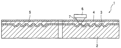
Fig. 1 shows a cross-section of an embodiment of the optical storage system
comprising an optical disk, an optical head device and a radiation beam that
is focused onto
the recording stack of the optical disk.
In Fig. 1 the optical storage system comprises an optical storage medium 1
that has a substrate 2. On a side thereof is deposited a recording stack 3
having at least one
CA 02469083 2004-06-02
WO 03/049098 PCT/IB02/05084
recording layer. A focused radiation beam 7, having a predetermined wavelength
and having
a predetermined numerical aperture, emanates from an optical head device 6. An
optically
transparent protective-coating stack 4 and 5 between the recording stack 3 and
the optical
head device 6 protects the recording stack 3 from impact by the optical head
device 6. The
5 protective coating stack 4 and 5 comprises a first layer 5, which has a
thickness of 9 nm. The
first layer 5 is made of the material Si3N4 and has a surface with a surface
energy smaller
than 1.5 J/m2. The pencil hardness of Si3N4 is harder than H. A second layer 4
is made of the
resinous material Daicure Clear EX-860 manufactured by Dainippon Ink &
Chemicals Inc. It
has a Young's modulus E of about 0.05 GPa. Spin-coating and subsequent UV-
curing, which
method is well known in the art, forms the layer 4, which has a thickness of
15 pm. The
present invention is not limited to this material. Other materials with a
Young's modulus
smaller than 10 GPa, for instance polymers or filled polymers, may also be
applied. Second
layer 4 may also be formed by adhering a sheet of transparent plastic, e.g.
polycarbonate (PC)
or polymethylinethacrylate (PMMA) provided with a layer of pressure sensitive
adhesive
(PSA), to the recording stack 3. First layer 5 is formed on second layer 4 by
sputtering. The
stoichiometry of Si3N4 may deviate slightly due to variation in sputtering
conditions. The
surface energy of layer 5 can be lowered by hydrogenation. Other possible
materials, which
may be used as the first layer 5 are silicon oxide, silicon oxynitride and
diamond-like carbon
(DLC), which have excellent wear-resistant properties. However, the present
invention is not
limited to these materials.
The surface energy of the materials of the first layer 5 should be smaller
than
1.5 J/m2, preferably smaller than 0.75 J/m2, and more preferably smaller than
0.1 J/m2.
Substrate 2 has a depression pattern corresponding to a servo pregroove or
information signals. Substrate 2 can, for instance, be made by injection
molding of a resin,
exemplified by polycarbonate (PC), or by injection molding of an UV-curable
resin on a
glass layer. The recording stack 3 is obtained by depositing, e.g. by
sputtering ,subsequent
layers on the surface of substrate 2 on which the depression pattern has been
formed. The
recording stack 3 may comprise a so-called phase-change recording layer, a
magneto-optical
recording layer or a dye layer. Other types of recording layers, e.g.
fluorescent layers, are not
excluded. Read-only (ROM) type layers, e.g. metals like aluminium, may also be
used.
Examples of phase-change materials are metals and alloys comprising one or
more of, e.g.
the elements Ge, Sb, In, Ga, Ag and Te. Examples of magneto-optical materials
are alloys
comprising e.g.Te, Ge, Fe and Co. The present invention can also be applied to
magneto-
optical recording systems with domain expansion read-out techniques, such as
magnetic
CA 02469083 2004-06-02
WO 03/049098 PCT/IB02/05084
6
amplifying magneto-optical system (1VIAMMOS) or domain wall displacement
detection
(DWDD).
If the surface stress of first layer 5 is larger than a critical surface
stress of
second layer 4, the surface of optical storage medium 1 will deform resulting
in an increased
surface roughness. A large surface roughness will adversely affect the optical
signal coming
from optical storage medium 1 as read out by the optical head device 6.
However, a slight
surface roughness can be advantageous since this will result in a reduction of
the contact area
between head and slider during impact. The surface stress of layers 5 and 4
can thus be tuned
to create an optical disk with a limited surface roughness. Limited surface
roughness means
that the optical signal from the optical disk 1 is not or only slightly
affected, while the contact
area between head and disk during impact is significantly reduced.
The resistance against damage of the preferred embodiment of the system by
impact of the optical head device 6 was tested by impact of a glass slider,
e.g. 6, onto the
optical storage medium 1. If layers 4 and 5 are not present, the surface of
the optical storage
medium 1 is severely damaged by impact with the glass slider 6. If only layer
5 is not
present, impact of the glass slider 6 results in visible permanent damage to
surface of the
optical storage medium 1 as well as extremely strong sticking of the slider
onto the surface of
the optical storage medium 1. If only layer 4 is not present, the glass slider
is visibly
damaged upon impact with the optical storage medium 1. If both layers 4 and S
are present,
no clear visible damage could be observed upon impact, neither on the optical
storage
medium 1 nor the glass slider 6.
It should be noted that the above-mentioned embodiments illustrate rather than
limit the invention, and that those skilled in the art will be able to design
many alternative
embodiments without departing from the scope of the appended claims. In the
claims, any
reference signs placed between parentheses shall not be construed as limiting
the claim. The
word "comprising", "comprise" or "comprises" does not exclude the presence of
elements or
steps other than those listed in a claim. The word "a" or "an" preceding an
element does not
exclude the presence of a plurality of such elements. The mere fact that
certain measures are
recited in mutually different dependent claims does not indicate that a
combination of these
measures cannot be used to advantage.
According to the invention an optical storage system, comprising an optical
storage medium and an optical head device, is provided. The medium is provided
with a
protective layer, which is very resistant to impact of the optical head device
without the use
of lubricants.