Note: Descriptions are shown in the official language in which they were submitted.
CA 02469371 2004-05-28
DIEhECTRIC SUBSTRATE WITH SE1~ECTIVEIrY CONTROIZED EFFECTIVE
PE&tMITTIVITY AND IaOSS 'TANl3ENT
DESCRIPTION OF THE REhATED ART
The design and fabrication of microwave circuits and
antennas are based on standard materials that are available
for printed wiring boards or ceramic substrates. Improvements
in the stanchrd materials are incremental and tend to be
infrequent. Attezr.pts at modifying the properties of the
substrates by various means have been attempted occasionally,
but they have not generally resulted in any process that is
practical, reliable and robust.
U.S. Patent No. 5,559,055 discloses a system for reducing
the interlayer dielectric constant in a multi.layer
interconnect structure to increase device speed and
performance. More particularly, the RC time constant of a
semiconductor device is reduced by decreasing' the capacitance
C. The decrease in capacitance is achieved by replacing the
interlayer silicon dioxide (dielectric constant of 4.0) with
air (dielectric constant of 1.0). In either case, the final
effective dielectric constant of the device is lowered, which
results in hLgher device speed.
U.S. Patent No. 6,175,337 discloses a high-gain,
dielectric loaded, slotted waveguide antenna. The antenna
makes use of a tailored dielectric structure in which the
effective dielectric constant is incrementally or continuously
reduced to have a dielectric constant close to that of the
free-space value at an outer surface a ckistance from the
waveguide array. The tailoring of the effective dielectric
constant is achieved by layering a given number of slabs of
different dielectric constants with sequentially reduced
values, or by varying the chemical composition of the
material, or by varying the density of the material imbedded
with high dielectr=~c constant particles.
-1-
CA 02469371 2004-05-28
Another approach to controlling the effective
permittivity of a dielectrir_ substrate is to perforate the
board material in selected areas. This approach could be
particularly well suited to ceramic substrates as they tend
have a relatively high loss tangent and are therefore lossy.
However, the perforating technique has also suffered from
certain drawbacks. For example, the perforation of the
substrate has tended to produce a weakened mechanical
structure, particularly when the percentage of substrate
material removed is high. Also, the perforations in the
substrate are open to the environment and can therefore allow
contaminants to caliect within the structure. The conventional
perforation techniques have also tended to produce dielectric
substrates with effective permittivity values that are not
consistent ac each measurable point on the surface.
Another disadvantage of conventional perforated substrate
system is that simply perforating the substrate will produce
openings on both sides of the board. Tzis irrterferes with the
RF circuitry disposed on the substrate. Perforations can be
drilled only partially through the substrate material to leave
a continuous surface on at least one side. for example, laser
drilling can be used for this purpose. However, difficulties
are encountered in controlling the accuracy of the laser
drilling process. Tn particular, it is difficult to precisely
control the depth of drilled perforations so as to maintain a
stable value of permittivity and loss tangent across the
surface of the perforated area. Moreover, the drilling
process leaves the internal structure of: the substrate exposed
on at least one side of the board.,
scn~t~ of SHE ~~NTao~
The invention concerns a method for fabricating a
substrate for an RF device. The method includes the steps of
forming a pattern of perforations in a plurality of layers of
-2-
CA 02469371 2004-05-28
a dielectric material in at least one perforated area of each
layer and arranging the plurality of layers in a stack. At
least one perforated area in each of the plurality of layers
is at least partially aligned with another perforated area of
another layer in the stack to lower an effective value of
permittivity and an effective value of a loss tangent in a
least one spatially defined region of the substrate, as
compared to a bulk value of permittivit.y and loss tangert for
the dielectric material. The layers can be formed from a low
temperature cofired ceramic tape or a high temperature cofired
ceramic tape. The method can also include the step of firing
the stack and forming an RF circuit component on the substrate
in the spatially defined regicn. The pattern of perforations
can be excluded from one or more outer layers of the substrate
to seal the inner perforations from dust and contamination.
According to one aspect of the invention, the perforation
pattern for each of the plurality of layers can be selected so
that the effective value of permittivity is substantially the
same at each measurable point of the spatially defined region
of the substrate. Further, the pattern can be varied among
the plurality of layers to ensure structural rigidity and a
final substrate with a planar outer surface. For example, the
pattern can be offset from layer to layer.
According to another aspect of the invention, the method
can also include selecting the pattern of perforations in the
plurality of perforated areas to produce different values for
the effective permittivity in a plurality of the spatially
defined regions on the substrate. Alternatively, the pattern
of perforations in each of the layers can be selected so as to
cause the effective permittivity to selectively vary in a
predetermined manner across a surface of the .substrate defined
by the spatially defined region.
The intention also concerns a substrate for an RF device.
The substrate is comprised of a plurality of layers of
-3-
CA 02469371 2004-05-28
dielectric material cofired in a stack. Each of the plurality
of layers is formed from a material having a permittivity and
having a pattern of perforations formed in at least one
perforated area. The perforated areas of each respective one
of the layers is advantageously aligned at least partially
with associated perforated areas in adjacent layers to lower
an effective value of a permittivity and an effective loss
tangent in one or more spatially defined regions of the
substrate. The substrate layers can be comprised of a high
temperature cofired ceramic tape or a low temperature cofired
ceramic tape.
BRIEF DESCRIPTION OF THE DRI~rWINGS
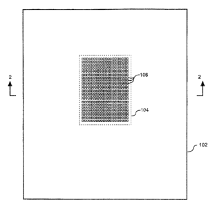
Fig. 1 is a top view of a single layer of a dielectric
material that can be used to construct a substrate with
selectively controlled effective permittivity.
Fig. 2 is a cross-sectional view of the single layer of
dielectric material taken along line 2-2 in Fig. 1.
Fig. 3 is a drawing that is useful for understanding the
assembly of a substrate.
Fig. 4 is a perspective view of the completed substrate.
Fig. 5 is a cross-sectional view of the completed
substrate taken along line 5-5 in Fig. 4.
Fig. 6A is an enlarged cross-sectional view of a portion
of the completed substrate in the area 6-6 in Fig. 5 showing
vertically s-caggered perforations,
Fig. 6E is an enlarged cross-sectional view of a portion
of the completed substrate in the area 6-6 in Fig. 5 showing
vertically aligned perforations.
DETAILED DESCRIPTION OF THE PREFERRED EI~ODIMENT
Referring to Figs. 1-3, a process is illustrated for
manufacturing a Laminated substrate formed from a plurality of
layers 102 having defined areas with selectively controlled
-4-
CA 02469371 2004-05-28
values of permittivity and loss tangent. Fig. 1 is a top view
of a layer 102 fo~~med of a dielectric material that can be
used to construct the substrate 300 shown in Fig. 3. A cross-
sectional view of the single layer 102, taken along line 2-2,
is shown in Fig. 2.
The layer 102 is preferably formed from an unfired
ceramic tape. According to a preferred embodiment, the layer
102 can be comprised of a low or high temperature type cofired
glass/ceramic tape. Glass/ceramic tapes such as those
IO described herein are well known in the art. For example, low
temperature 951 cofire Green TapeTN can be used for this
purpose. Green TapeTr' is Au and Ag compatible, has acceptable
mechanical p;~operties with regard to thermal coefficient of
expansion (TCE) and relative strength. zt is available in
I5 thicknesses ranging from 114 um to 254 um and is designed for
use as an insulating layer in hybrid circuits, multichip
modules, single crip packages, and ceramic printed wire
boards, including RF circuit boards. Low temperature 951
cofire Green Taper' is available from The DuPont Company's
20 Microcircuit Materials division which is located at 14 T.W.
Alexander Drive, Research Triangle Park, NC.
As used herein, the reference to low temperature cofired
ceramics refers to ceramics that can be fired at relatively
low temperatures. For example; firing temperatures for such
25 material range are typically less than about 850 degrees
Centigrade. By comparison, high temperature ceramics are
typically fired at temperatures in exceas of 1500 degrees
Centigrade.
A typical electronic circuit module can be made with
30 Green Tape by cutting tape foil to size, punching vias and
filling same with thick film conductive paste. Subsequently,
the conductive interconnect lines are patterned on the tape.
The operation is repeated multiple times if additional layers
are required. After all of the individual layers are
-5-
CA 02469371 2004-05-28
complete, they can be collated, stacked., and laminated. At
this point the stacked layers are commonly referred to as a
"green" multilayer. Using standard processing techniques, the
multilayer is fired and cut to size. finally, the top layer
is completed by forming resistors, and gold and silver bearing
conductors.
Although low and high temperature cofired glass/ceramic
substrates are preferred for use in the present invention, it
should be noted that other dielectric substrate layers can
IO also be used and the invention is not intended to be limited
in this regard. F~ preferred thickness of the layers 102 is
presently between about 100um to 300um, but :it should be
understood tizat layers that are thinner or thicker can also be
used.
According to a. preferred embodiment of the invention
illustrated in Figs. 1 and 2, each layer 102 can have one or
more perforated areas 104 which are formed with a pattern of
very small perforations 106. At least one perforated area in
each of the layers 102 is preferably at least: partially
aligned with at least one other perforated area of another
layer 102 in the stack. This will lower an effective value of
a permittivity and an effective value o:f a loss tangent in a
spatially defined region of the substrate coincident with the
aligned portion of the perforated areas as compared to a bulk
value of perr~ittivity and loss tangent for th.e dielectric
material. Perforated areas are considered to be at least
partially aligned when at least a portion of a perforated area
104 for a layer 102 overlaps at least a portion of a second
perforated area of another layer in the stack.
The perforations 106 are preferably formed in each layer
102 while the layer is still in the pre--fired state. The
pattern, size, shape and spacing of the perforations 106 are
selected to adjust the effective permitt:ivity and effective
loss tangent in the perforated areas. The shape of the
_6_
CA 02469371 2004-05-28
perforations is not. critical to the invention. However,
square perforations are presently preferred relative to
circular perforations because of the larger amount of material
that can be effectively removed while still :maintaining
structural integrity of the layer. If the perforations 106
have a square outline, they can be in the range of about .004
inches to 0.2 inches on each side, depending on the wavelength
of the RF si4nals of interest in a particular application. In
general, the size of the perforations is preferably no larger
than about 1/10A to 1/50A, where A is equal to one wavelength
at the frequency of interest. The relative size selected will
be dependent somewhat on the frequency of interest and
fabrication limits. For example, at lower frequencies and/or
with improved fabrication techniques, perforations less than
1/50A are possible. In fact, the concept works for any size
scale below the previously mention 1/10 limY_t and can be
realized even down to the nanoscale level with the same bulk
properties.
The perforations 106 can be formea'. by punching or
drilling each layer separately using commercially available
equipment. According to a preferred embodiment, commercially
available precision computer controlled high speed punching
equipment can be used for this purpose. For example, the
perforations can be formed using an MP 4150 type automated
punch available from Unichem Industries, Inc. of San Clemente,
CA. Computer controlled high speed punching equipment is
preferred for this process because the pattern of perforations
106 in perforated area 104 can vary somewhat from layer to
layer. For example, the arrangement of perforations, their
spacing and shape may be varied. Alternatively, the
perforations can be vertically aligned or can be simply offset
slightly from one layer to the next while maintaining
essentially uhe same pattern.
CA 02469371 2004-05-28
It is possible for the perforation pati~ern in layers 102
to be varied from layer to layer or they may be aligned
directly with the perforations in the layer above and below
without affecting the planarity of the t:op or bottom surface.
Structural rigidity is retained by applying either approach to
arranging the perforated layers.
The effective permittivity of the perforated area
generally decreases linearly as more substrate is removed.
Significantly, however, it has been found that the effective
loss tangent for the perforated area 109 will decrease
rapidly, and in a non-linear fashion, as the percentage of
material comprising layer 102 that is removed ranges from
about 60o to 900. The optimal volume of substrate removed
will depend upon a variety of factors. For example,
consideration must be given to the increasing fragility of the
structure as larger amounts of material are I°emoved. Also,
care must be takers so that the perforated area 104 does not
create a non-planar outermost surface 114 when the layers 102
are arranged in a stack.
Referring again to Fig. ~, at least one outermost
dielectric layer 108 can be formed from the same material as
the layers 102 and added to the stack of layers 102 as shown.
However, the outer dielectric layer 108 is preferably devoid
of perforated areas 104. In this way, i~he outer dielectric
layer 108 can act as a sealing layer to prevent the intrusion
of dust, moisture and other contaminants into the perforations
106 in the layers 102. Depending upon the electrical and
mechanical requirements for a particular application, it can
be desirable to include multip7_e dielectric layers 108. The
additional layers can provide increased rigidity and
mechanical strength as may be required depending upon the
intended use and environment (such as shock and vibration).
Once all of the dielectric layers have been arranged in a
_g_
CA 02469371 2004-05-28
stack, they can be fired in a manner consistent with the
requirements of the particular type of layer material.
After firing, the stack of layers 102, 108 can be
arranged on a base 112. According to a preferred embodiment,
base 112 is a conductive sheet or foil. For example copper
sheet can be used for this purpose. However, it should be
understood that the invention is not sc> limited and a rigid
dielectric or semiconductor material can also be used to form
base 112. An adhesive layer 110 is preferably provided
between the layers 102 and the base 112 to secure the stack of
dielectric layers to the base 112. Adhesive layer 110 is
preferably a conductive adhesive. For example an electronic
grade conductive film adhesive can be used for this purpose.
Such adhesive is typically a silver filled epoxy with 700
silver particles. Adhesives of this type are commercially
available and can be cured at relatively low temperatures.
For example, typical curing times are about 125 degrees
centigrade for about 2 hours in a low temperature cure oven.
Curing time will vary depending on the ;pari:ic:ular adhesive
material than is selected.
Once the cured stack of layers 102, 108 have been placed
on the adhesive 110, they are preferably maintained in a
stationary position until the adhesive l7as cured. Sliding or
moving the perforated layers 102 can cause tree conductive
adhesive to be inadvertently forced up into the perforations
106, thereby negatively affecting the electrical performance
of the substrate 300. According to an alternative embodiment,
one or more solid dielectric layers 109 made from the same
material as layers 102 but without any perforations can
optionally be interposed between the lowermost layer 102 and
adhesive laye>r 110. The solid dielectric layer 209 can be
used to prevent the unwanted intrusion of the adhesive layer
110 into the perforations 106. Also, such layers can be
desirable for improved mechanical properties as may be
-9-
CA 02469371 2004-05-28
necessary de;~ending upon the .intended use and environmental
conditions.
Fig. 4 is a cross-sectional view of a completed substrate
300 with selectively controlled permitt;ivity. Fig. 5 is a
cross-sectional view through substrate 300 taken along line 5-
5. The substrate 300 includes one or more spatially defined
regions 504 that have a lower effective value of permittivity
and a lower effective value of loss tangent, as compared to a
bulk value of permittivity and loss tangent for the dielectric
material comprising the layers 102, 108. The lower values are
due to the selective removal of dielectric material as shown.
Fig. 6a is an enlarged view of a portion of Fig. 5
defined by line 6--6 showing ars offset perforation pattern from
one layer 102 tc the next layer 102 as previously described.
Notably, this can result in vertically staggered perforations
as shown. However, the invention is not lim_Lted in this
regard, and it is also possible to form perforated areas that
make use of a consistent pattern from one layer to the next so
as to produce vertically aligned perforations as illustrated
in Fig. 6B. In yet another embodiment, the patterns can vary
from layer to layer while remaining within the perforated area
of each layer 102.
Conductive elements 116 can be screen painted on
outermost layer 108 on an area of outermost layer 108
extending over spatially defined region 504. The screen
printing on the array is typically an e7_ectronics grade
conductive epoxy or ink that cures in the 100 degree to 125
degree range. The conductive elements 116 can comprise any of
a wide variety of Ff elements that have an electrical
characteristic modified as a result of the modified
permittivity and/or loss tangent of the spatially defined
region 504. For example, and without limitation, conductive
elements 116 can be antenna elements associated with an array,
-10-
CA 02469371 2004-05-28
filter elements, transmission line elements, transformer
elements, stubs, and so on.
The foregoing process offers great flexibility for RF
designers without requiring costly changes to conventional
processing methods. Having made the fundamental choice of the
dielectric t:lickness, selected portions of the substrate can
now be specie,°_ically tailored to achieve the desired dielectric
properties. The flexibility of this approach gives the RF
designer almost unlimited control over effective permittivity
and effective loss tangent without changing processing steps.
According to one aspect of the invention, the perforation
pattern for each of tha plurality of layers can be selected so
that the effective value of permittivity is substantially the
same at each measurable point of the spatially defined region
of the substrate. Further, a multiplicity of spatially
defined regions 504 can be defined within the substrate, each
with either the same or different effective values of
permittivity and loss tangent. Alternatively, the pattern of
perforations in each of the layers 102 can be selected so as
to cause the effective permittivity and loss tangent to
selectively vary in a predetermined manner across the surface
114 of the substrate defined by the spatially defined region.
This can include varying the perforation size, perforation
shape and/or perforation spacing within the perforated area
104 of one or more layers 102. For example, progressively
more or less dielectric material can be removed from one or
more layers 102 along a particular direction defined along the
surface 114 so as to cause the permittivity and loss tangent
to decrease or increase in a predetermined manner. In any
case, the perforation pattern can be Varied among the
plurality of layers to ensure structural rigidity and a final
substrate 30J with a planar outer surface 114.
-11-