Note: Descriptions are shown in the official language in which they were submitted.
CA 02469529 2004-06-02
SYSTEM AND METHOD FOR IMPROVING CONNECTIVITY
OF MULTIPLE PARALLEL CONNECTORS
Field of the Invention:
The present invention relates to a multiple parallel conductor, in particular,
to a
continuously transposed cable, used for windings of electrical devices, such
as
transformers, with a plurality of strands, wherein each strand has a separate
electrical
insulation capable of easily being stripped for connectivity preparation.
Background:
The majority of modern electrical devices and machines. specifically high
power
transformers, employ continuously transposed cables, known as CTC. A
continuously
transposed cable with a specified cross section has a number of mechanical and
electrical
advantages compared to a traditional cable of the same cross section and made
of an
individual conductor.
A continuously transposed cable is composed of a Iarge number of strands,
wherein each strand has a separate electrical insulation. The strands are
connected in
parallel at the ends. Furthermore, in the CT cables, also known as Roebel
rods, the
strands have an,approximately rectangular cross section. Each strand includes
an
insulating varnish covering a conductor made of copper, aluminum or an alloy
thereof.
The strands; each having their own electrical insulation, are combined into a
bundle so as
to define an approximately rectangular cross section.
1
CA 02469529 2004-06-02
Typically, the magnetic wire insulation used on the strands in the multiple
parallel
conductors is an applied layer of polyvinyl coatings or polyvinyl acetyl
resins, siuch as the
commonly used Formvar@.
In addition to the insulaticm coating on the individual strands, an additional
layer
of epoxy, such as epoxy resin, may be bonded to the strands to improve cable
lifespan in
response to operation in very high power conditions. Typically, transformers
that are
continuously subjected to overload conditions experience a high level of
mechanical
force generated by electromagnetic effects. These forces interact to cause
cable strand
twisting, which results in a significant shorter lifespan for the cable. The
epoxy bond
lo covering the Fornivar layer causes the bundle to behave as one integrated
unit so that
the strands experience a lesser amount of twisting against each other. .
When used in transformers, each strand of the multiple parallel conductor of a
continuously transposed cable needs to be prepared for proper electrical
connections. In
order to make these connections, the insulation and epoxy needs to be stripped
off of each
of the individual strands in the cable before they are soldered to other
electrical nodes.
This process is extremely time consuming and requires a significant amount of
human
resources to be devoted to such a process.
Typically, a current stripping method employs mechanical removal by cutting
off
the insulation layer with a wire brush or a?cnife. Another approach is to
remove the
20 insulation by heat decomposition using a flame torch for example. Yet
another method is
to use chemicals such as alkali to reniove the insulation strip. Finally,
there has been
attempts to remove the insulation layer by solder by decomposing it inside a
molten
solder bath.
2
CA 02469529 2008-06-19
None of the above methods have proven satisfactory. Therefore, there
exists a need for manufacturing a cable, for use with transformers or other
electrical devices, wherein the stripping and cleaning of the individual
strands
can be done quickly and effectively, reducing the amount of time needed to
properly electrically connect the cables to other electrical nodes.
Summary Of The Invention:
It is therefore an object of the invention to provide an improved multiple
parallel conductor for windings of electrical devices and machines that
provides
a simplified means for stripping and preparing the ends of the multiple
parallel
conductor cables for electrical connection to an electrical node.
The invention can be broadly summarized in that at least one layer of
solderable material is disposed over the conductor in each strand before any
insulation or epoxy is applied, so that when the end of the cable is placed
into a
solder bath, the solderable layer and all of the layers of insulation and
epoxy on
the strands are removed, quickly exposing the bare strands to be cleaned and
inserted into the desired connection.
Thus according to one aspect of the invention there is provided a multiple
parallel conductor of the continuously transposed cable type for use in
electrical
devices, said multiple parallel conductor comprising:
a plurality of strands, wherein each of said strands further comprises;
a conductor;
a solderable enamel layer, disposed on at least a portion of said
conductor; and
an insulating varnish layer, disposed on said solderable enamel layer,
such that when said piurality of metal strands are placed into a solder bath,
said
insulating varnish layer is removed from said conductor.
Another aspect of the invention concerns a multiple parallel conductor of
the continuously transposed cable type for use in electrical devices, said
multiple parallel conductor comprising:
a plurality of strands, wherein each of said strands further comprises;
3
CA 02469529 2008-06-19
a conductor;
a protective layer, disposed on at least a portion of said conductor; and
an insulting varnish layer, disposed on said protective layer, such that
when said plurality of metal strands are treated, said protective layer and
said
insulating varnish layer are removed from said conductor.
Still another aspect of the invention concerns a method for producing a
multiple parallel conductor for use in electrical devices having a plurality
of metal
strands, said method comprising steps of:
providing a conductor for each of said strands;
applying at least one layer of solderable enamel to at least one of said
plurality of said conductors; and
applying at least one layer or insulating varnish to said layer of solderable
enamel such that when said one of said plurality of metal strands is placed
into a
solder bath, said insulating varnish layer is removed from said conductor.
Yet another aspect of the invention concerns a method for stripping a
strand of a multiple parallel conductor having a plurality of strands, wherein
said
strands have a conductor, a solderable enamel layer and an insulating varnish
layer, said method comprising steps of:
preparing a molten solder bath;
submerging said strands into said solder bath; and
melting said insulating varnish layer completely away from said strand
into said solder bath.
3a
CA 02469529 2004-06-02
Brief Description of the Drayyines:
Figure 1 is a perspective view of a first embodiment of a multiple parallel
conductor madc in accordance with the invention;
Figure 2 is a front cross-sectional view of a second embodiment of the
multiple
parallel conductor of figure 1, having a varicd support tapc, in accordance
with one
embodiment of the present invention;
Figure 3 is a longihtidinal cross sectional view of a strand from the multiplc
parallel conductor of figure 1, in accordance with one embodiment of the
present
invention;
Figure 4 is a front cross sectional view of the strand from the multiple
parallel
conductor of figure 3, in accordance with one embodiment of the present
invention;
Figure 5 is a flow chart illustrating the process of applying layers to the
multiple
parallel conductor from figure 3, in accordance with one embodiment of the
present
invention;
Figure 6 is a diagram of a solderable enamel layer being applied to a multiple
parallel conductor as shown in figure 3, in accordance with one embodiment of
the
present invention;
4
CA 02469529 2004-06-02
Figure 7 is a flow chart illustrating the process of stripping the multiple
parallel
= conductor from figure 1, in accordance with one embodiment of the present
invention;
and
Figure 8 is an expanded side cross section view of the strand of the multiple
paralle] conductor of figure 3 with thc ends of the slrrsncls having been
stripped, in
accordance with one embodiment of the present invention.
CA 02469529 2004-06-02
Detatled DescrintiaA of the Invention:
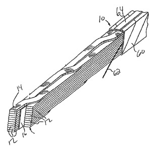
Figs. 1 and 2 illustrate a multiple parallel conductor 10 for windings of
electrical
motors, including transformers, having a bundle of individual insulated
transposed
strands indicated as 12. Transposed strands 12 cross over one another as
described in
U.S. patent number 5,962,945, the entirety of which is incorporated herein by
reference.
Strands 12, having a conductor material 18, are arranged, for example, in two
juxtaposed
stacks 14, with a paper tape 16 extending in the. longitudinal direction
between the two
stacks 14, as is shown in Fig. 1.
As illustrated in Figs. 3 and 4, cach onc of strands 12 is coated with a
solderable
enamel layer 20, applied directly to conductor 18. Solderable enamel 20 is
applied in
coats evenly across the entire surface of conductor 18. Solderable enamel
layer 20 can be
applied to conductor 18 in any number of conventional methods such as with the
usc of a
metering die. The thickness of solderable enamel layer 20 may vary depending
on the
type of insulation to be deposited on top of it. However, it is typically
applied in a
manner' and a thickness that is aimed to prevent oxidatinn during or after the
application
process. For instance, oxidation may degrade the adhesion between conductor 18
and
solderable enamel layer 20.
In accordance with one embodiment of the present invention, solderable enamel
layer 20 is a applied in a single layer, curing to a fuial thickness of 0.0004
inches thick.
This process can be done for each single strand 12 individually, or in a mass
production
process to multiple strands 12 simultaneously.
6
CA 02469529 2004-06-02
It should be noted that solderable enamel layer 20 is acting in the function
of a
protective layer between conductor 18 and an insulating varnish layer 30.
Thus, any
protective layer having similar properties for use with similar multiple
parallel conductor
is also witliin the conternplation of the present invention. However, for the
purposes
of illustrating the salient features of the present invention, solderable
enamel layer 20 is
used.
Solderablc cnamcl layer 20 niay be applied in several coats or it can be
applied in
a single coating. The thickness of layer 20 may be varied to accommodate
various types
of metals used for conductor 18 of strand 12 as well as to accommodate various
types of
10 insulation to be applied thereto, provided that soldcrablc enamcl 20 is
able to parform its
functions as described in more detail below.
As illustrated in Figs. 3 and 4, each strand 12 is provided with its own
insulating
varnish layer 30, to ensure adequate electrical insulation between the
adjacent strands 12.
For example; a typical insulating varnish layer 30 may be any polyvinyl
coatings or
polyvinyl acetyl resins such as Formvar or any other similarly suited
insulator that
meets the insulating properties required by multiple parallel ccmductors 10.
For the
purposes of illustration of the salient features of the present invention,
insulating varnish
layer 30 will be assumed to be Formvar coating, however this is in no way
intended to
limit the scope of the present invention. Any similar insulating material may
be utilized
in conjunction with strands 12 is within the contemplation of the present
invention.
Insulating varnish layer 30 can be applied to strand 12 in any number of
conventional methods. As illustrated in Fig. 3, insulating varnish layer 30 is
applied on
top of solderable enamel layer 20 after that layer is set or cured, such that
insulating
7
CA 02469529 2004-06-02
vamish layer 30 results in an insulation that preferably does not directly
contact
conductor 18 of strand 12.
The thickness of insulating varnish layer 30 may vary depending on the
insulation
rcquircments for strands 12, however it is lypically applied in individual
coats that, when
cured, are 0.0004 inches thick. In a typical application for strand 12,
somewhere between
six and ten coats of insulation material or Formvar are applied in order to
form
insulating varnish layer 30.
In one embodiment of the present invention, as illustrated in Figs. 3 and 4,
to =
improve the mechanical strength of the electrical insulation varnish layer 30,
an
additional coating of a partially cross-linked epoxy varnish 40 ean also be
applied over
insulating vamish coating 30 of each strand 12. Epoxy layer 40 can be applied
to strand
12 in any number ot'conventional methods. As illustrated in Figs. 3 and 4,
epoxy layer
40 is applied on top of insulation varnish layer 30 after the final coat of
that layer is dry.
This epoxy layer 40 results in a hardened epoxy or bond that rests on top of
the insulation
varnish layer 30 of strand 3.
The thickness of epoxy layer 40 may vary depending on the desired added
strength to be added to strands 12, however it is typically applied in
individuat coats that,
when dry, are 0.0004 inches thick. In a general application for strand 12,
somewhere
between 2 and 4 coats of epoxy are applied in order to forni epoxy layer 40.
Along with insulating varnish layer 30 and solderable enamel layer 20, the
thickness of epoxy layer 40, may be set to meet industry standards for
multiple parallel
conductors 10 such as NEPA (National Environmental Policy Act) and IEC
(International
Electrotechnical Commission).
8
CA 02469529 2004-06-02
It is noted that epoxy layer 40 is not required for proper operation of
strands 12,
but is included as an optional layer for illustration purposes only. Strands
12 with only
solderable enamel layer 20 and insulation vamish layer 30 are also within the
contemplation of the present invention.
As illustrated in Figs. 1 and 2, after each strand 12 is properly coated with
solderable enamel layer 20, insulating varnish layer 30 and epoxy layer 40,
strands 12 are
formed into multiple parallel conductors 10, such as continuously transposed
cabics for
use in transformers. Additional elements may be added at this time to improve
the
quality of multiple parallel connectors 10.
For example, common wrapping 60, made of paper tapes, is placed over the
bundle of electrically insulated strands 12 formed in this manner. A fiu-ther
element for
improving multiple parallel conductors 10, illustrated in Figs, 1 and 2,
includes a rip cord
62 underneath wrapping 60, extending in the longitudinal direction along the
entire
length of the multiple parallel conductor 10, so that the wrapping 60 can be
removed
easily and cost-effectively during manufacture of the windings for electrical
devices and
machines, i.e. at the same time when the continuously transposed cables are
wound.
Yet another element for improving multiple parallel conductors 10, illustrated
in
Fig. 1, includes a support tape 64. On the outside of the common wrapping 60
of strands
12, support tape 64 is disposed, that extends in the longitudinal direction of
the multiple
parallel conductor 10 and which is coated with an adhesive and affixed to the
wrapping
60. Support tape 64 has the purpose to hold the individual elements of
wrapping 60
together after the rip cord is torn, so that the wrapping 60 can be removed
easily and
completely without contamination from loose constituents of the wrapping.
9
CA 02469529 2004-06-02
in the embodiment illustrated in Fig. 2, support tape 64 extends parallel to
the
longitudinal direction of multiple parallel conductor 10, but is placed
between one of the
stacks of strands 12 and the inside of the wrapping 60 on that side of the
multiple parallel
conductor 10 which faces away from rip cord 62. A more thorough description of
these
and other improvements for multiple parallel conductor 10 can be found in U.S.
Patent
No. 5,962,945, the entirety of which is incorporated herein by reference.
In one ombodiment of the presciit invention as illustrated in Fig. 6, a cable
assembly line 300 is provided. Assembly line 300 comprises a roller 302
containing bare
conductor 18. Conductor 18 is spun off of roller 302 then through an in-line
annealer 304
for applying the soldera.ble enamel in an appropriate thiolmcas by way of a
metering die
or other such manufacturing device. Positioned after in-line annealer 304, an
RO
(Reverse Osmosis purified) water bath 306, sponge wipes 308 and air dryer 310
are
configured to remove exccsa soldeiiable enamel and provide initial cooling for
conductor
18 and solderable enamel layer 20.
An enamel oven 312 is positioned at the end of assembly line 300 so that
conductor 18, having the just applied solderable enamel thereon, revolves on
cnntinunus
rollers through oven 312 until the solderable enamel dries into solderable
enamel layer
20. An application device 314 is positioned outside of enamel oven 312 so that
after
solderable enamel layer 20 is cured, insulating vamish and epoxy may be
applied to form
insulating varnish layer 30 and epoxy layer 40, to be dried and cured in the
same enamel
oven 312. The process for each step in the application process is described in
more detail
below.
CA 02469529 2004-06-02
In one embodiment of the present invention as illustrated in flow chart of
Fig. 5,
strands 12 are generated for use in multiple parallel connector 12. At step
200, a
conducting material is chosen to form conductor 18 of strand 12. After the
material is
sclccted, such as copper, at step 202, conductor 18 is drawn and milled into
the proper.
thickness and shape to form multiple parallel conductor 10, such as flattened,
substantially rectangular, strips for use in continuously transposed cables.
Conductor 18
is then loaded onto rollers 302.
Next, at step 204, a solderable enamel is placed onto conductor 18 of strand
12.
In order to prevent oxidation, the entire surface of conductor 18 is covered
quickly. The
solderable enamel used in solderable enamel layer 20 is applied in liquidized
fortn. As
illustrated in Fig. 6, at step 206, conductor 18 is drawn under a metering die
within in-
line annealer 304 so as to remove the excess solderable enamel, so as to form
the
unifotmly thick solderable enamel layer 20 on conductor 18. As discussed
previously,
the metering die is set so as to form a solderable enamel layer 20 that, when
cured, is
substantially 0.0004 inches thick, however, this thickness may be adjusted as
necessary.
Next at step 208, conductor 18, having solderable enamel layer 20 deposited
thereon, is then moved into enamel oven 312 where solderable enamel layer 20
is
allowed to set before applying the insulating varnish. The temperature of
enamel oven
312 is set so as to provide adequate curing of layer 20.
After all of the coats of solderable enamel are cured onto conductor 18,
forming
the ftnished solderable enamel layer 20, at step 210, the insulating varnish
is applied by
application device 314 to the set solderable enamel layer 20 so as to form
insulating
varnish layer 30. The insulating varnish is applied to solderable enamel layer
20 at a
11
CA 02469529 2004-06-02
tcmperature below that which would melt solderable enamel layer 20. At step
212, the
insulating varnish is applied in a coat and dried in enamel oven 312 so that,
when cured,
it is-approximately 0.0004 inches thick. As described above, insulating
varnish layer 30
is applicd to solderable er.iarnCllayer 20 and, as such, does not direetly
contact conductor
18. This makes the subsequent removal of insulating varnish layer 30, by way
of solder
bath, easier and more efficient
Next, at step 214, thc procoss of applying coats of insulaling material to
strand 12
is repeated in stages until the desired thickness of insulating vanush layer
30 is complete,
After insulating varnish layer 30 is complete, and the last coat of insulating
material is
dried at a temperature for delivering adequate curing, at step 216 the cpoxy
is added by
application device 314 in similar process as outlined above. At step 218, the
coating step
is repeated, placing coats of epoxy onto strand 12 and dried in enamel oven
312 so that
when cured, they are 0.0004 inch thick, until the final desired thickness of
epoxy layer 40
is reached. Epoxy layer 40 is dried at a temperature sufficient to cause
adequate curing.
Once solderable enamel layer 20, insulating varnish layer 30 and epoxy layer
40
are secured and dried onto conductor 18 of straad 12, the completed strands 12
are combined into multiple parallel connector 10 as illustrated in Figs. I and
2.
It is noted that the thickness of the coats that form solderable enamel layer
20,
insulating varnish layer 30 and epoxy layer 40, the duration and temperature
for drying
each coat as well as the final thickness of those layers may vary based on a
number of
factors including the ultimate use for strand 12 and the raw materials being
used for the
layers. However, any similar strands 12 created using similar methods, having
a
solderable enamel layer are within the contemplation of the present invention.
12
CA 02469529 2004-06-02
After the manufacture of multiple parallel conductor 10 is complete, it is
ready for
use in applications such as for use in high voltage traasformers. It is noted
that there are
many uses for the multiple parallel conductor 10, as described above, however,
for the
purposes of illustra.tion, it will be described herein in connection with its
use in power
transformers.
Before multiple parallel conductoc 10 can be properly utilized, it must be
prepared
for insertion/connection with external clcctrical nodes. To do this, each
slranei 12 must
be stripped (have the insulation removed) so that conductor 18 of strand 12
can directly
contact the electrical nodes. In the prior art, each individual strand 12
needed to be
stripped tn an appropriate length, between 4"-S" from the end, for every
strand.12 in
multiple parallel conductor 10. The present invention greatly reduces the
labor required
for such stripping procedure following the method outline below.
In one embodiment of the present invention, as illustrated in the flow chart
of Fig.
7, at step 100, multiple parallel conductor 10, as illustrated in Figs. 1 and
2 is prepared
for insertion into an electrical node by way of removing of wrapping 60 using
rip cord
62. Next, at step 102, a molten solder bath is prepared having enough
liquidized solder to
strip strands 12 to the appropriate length. The solder bath should be round
enough to
accommodate the entire the entire cross section of multiple parallel conductor
10 and
deep enough to strip approximately 4-8 inches from strand 12.
The solder bath is heated to a degree sufficient to remove epoxy layer 40,
insulating varnish layer 30, and solderable enamel layer 20. Preferably, the
solder bath is
heated to approximately 480 degrees centigrade. This is intended only as an
example of
one temperature that can be used, however, other temperatures, sufficient to
remove all of
13
CA 02469529 2004-06-02
the layers 20, 30 and 40 from strand 12 without being too hot so as to damage
the metal
also may be used as desired. The optimum temperature may vary based on the
different
materials used to form solderable enamel layer 20 and insulating varnish layer
30.
At step 104, the end of multiple parallel conductor 10 is dipped into the
solder
bath to a level such that the amount of insulating varnish layer 30 and epoxy
layer 40 to
be stripped from the end of strands 12 is submerged in the solder. It may be
advantageous to slightly space or luoscn strands 12 from one another so as to
allow the
molten solder in the solder bath to act equally on all of strand 12 of
conductor 10.
Next at step 106, multiple parallel conductor 10 is held in the solder bath
until the
bare wire of strands 12 are cleared of any coatings. Exposure to thesa
tcinperatures
causes both epoxy layer 40 and insulating varnish layer 30, such as p'ormvar ,
to melt
away from solderable enamel layer 20 at a rapid rate. Then, as the strands 12
approaches
the full temperature of the solder bath, solderable enamel layer 20 liquefies
and becomes
separated from the metal of strand 12 as well.
Alternatively, if tinning is desired, some of solderable enamel layer 20 may
be left
on the ends of strands ] 2 so as to strengthen the eventual soldered
cnnnection with the
desired device. Typically each strand 12 requires about 20 seconds in the
solder bath to
remove epoxy layer 40, insulating varnish layer 30 and solderable enamel 20.
However,
when combined strands 12 from multiple parallel connector 10 are placed
together in the
solder bath, the time needed for proper stripping of all strands 12 is
approximately 2
minutes. The duration for which strand 12 is held in the solder bath may very
based on
the melting properties and the thicknesses of layers 20, 30 and 40 as well as
if tinning is
desired.
14
CA 02469529 2004-06-02
After all of materials sought to be stripped are removed as illustrated in
Fig. 8, at
step 108, multiple parallel conductor 10 is removed from the solder bath and
is cleaned.
The cleaning can be done in any method capable of removing any residual solder
of
sUlderable enamel layer 20 from strands 12, including cleaning with an
abrasive material
or wire brush. If tinning of strands 12 is desired then solderable enamel
layer 20 or a
portion thereof may be left on strand 12, and cleaning by the above process is
used to
remove only excess iusulatiag varnish layer 30 or epoxy layer 40 residue. The
process is
completed at step 110 when all of the excess materials are removed and strands
12 are
clean and coupled to the desired electrical connection.
ThB embodiments described above rcmarkably achieves the objects oftl-e
invention. However, it will be appreciated that departures can be made by
those skilled in
the art without departing from the spirit and scope of the invention which is
limited only
by the following claims.