Note: Descriptions are shown in the official language in which they were submitted.
CA 02469870 2010-01-27
HIGH PERFORMANCE FLUORESCENT OPTICAL SENSOR
BACKGROUND OF THE INVENTION
Field of the Invention
[0002] This invention relates generally to sensor devices for detection
of electromagnetic emissions from an indicator having an analyte of interest
permeating therethrough, wherein the characteristics of the emissions vary as
a
function of the concentration of the analyte. More particularly, the invention
relates to improvements in the design and performance of such sensor devices.
Background Art
[0003] U.S. Patent No. 5,517,313 describes a fluorescence sensing
device comprising a layered array of a fluorescent indicator molecule-
containing matrix (hereafter "fluorescent matrix"), a high-pass filter and a
photodetector. In this device, a light
1
CA 02469870 2004-06-09
WO 03/050519 PCT/US02/39675
source, preferably a light-emitting diode ("LED"), is
located at least partially within the indicator
material, such that incident light from the light
source causes the indicator molecules to fluoresce.
The high-pass. filter allows emitted light from the
indicator molecules to reach the photodetector, while
filtering out scattered incident light from the light
source. An analyte is allowed to permeate the
fluorescent matrix, changing the fluorescent properties
of the indicator material in proportion to the amount
of analyte present. The fluorescent emission is then
detected and measured by the photodetector, thus
providing a measure of the amount or concentration of
analyte present within the environment of interest.
[0004] One advantageous application of a sensor
device of the type disclosed in the '313 patent is to
implant the device in the body, either subcutaneously
or intravenously or otherwise, to allow instantaneous
measurements of analytes to be taken at any desired
time. For example, it is desirable to measure the
concentration of oxygen in the blood of patients under
anesthesia, or of glucose in the blood of diabetic
patients.
[0005] Since the invention of the device described
in the `313 patent, the present inventors have
developed a number of design improvements which have
significantly enhanced the performance, reliability and
longevity of optical sensor devices of the type
described in the `313 patent.
[0006] In particular, because of the size and
weight restrictions placed on such sensor devices
especially for in-vivo or in-situ applications, it is
2
CA 02469870 2004-06-09
WO 03/050519 PCT/US02/39675
important to maximize the efficiency of the available
indicator matrix in order to obtain a more reliable and
accurate measurement signal, while minimizing power
consumption and heat generation. Additionally, the
sensor device design should permit cost-effective high
volume manufacturing at a reasonable selling price.
Further, maximizing the longevity of the device is
desirable especially where the device must be implanted
in the body for in-situ detection of bioanalytes.
3
CA 02469870 2004-06-09
WO 03/050519 PCT/US02/39675
SUMMARY OF THE INVENTION
[0007] In accordance with an aspect of the present
invention, an optical sensor device for determining the
presence or concentration of an analyte, is provided,
including a substrate; a light-shielding baffle layer
formed on the substrate, and containing at least two
cavities therein; a light source for emitting light
primarily of a preselected wavelength upon
energization, mounted on a surface of the substrate in
one of the cavities; a light detector for detecting
light incident thereon and generating an electrical
signal responsive thereto, mounted adjacent to the
light source on the surface of the substrate in another
of the cavities, and being separated therefrom by the
light shielding baffle; a waveguide formed over the
light source and the light detector, wherein the light
source-containing cavity is filled with a transparent
epoxy material having the same refractive index as the
waveguide, such that the light source may be considered
to be located "within" the waveguide; the waveguide
having a mean thickness corresponding to a far field
emission point of the light source as determined by the
light source's position relative to the light shielding
baffle, the intrinsic emission profile of the light
source, or a combination of the relative position and
intrinsic emission profile; and an analyte-permeable
indicator matrix disposed on an outer surface of the
waveguide, the fluorescent matrix containing
fluorescent indicator molecules whose fluorescence is
attenuated or enhanced by the presence of analyte in
said fluorescent matrix, the preselected and
fluorescent indicator molecule being selected such that
4
CA 02469870 2004-06-09
WO 03/050519 PCT/US02/39675
the wavelength emitted by the light source excites
fluorescence in the indicator molecules; wherein the
light detector generates an electrical signal
responsive to fluorescent light incident thereon
emitted by said fluorescent indicator molecules. The
photodetector cavity is filled with a color-doped
material which acts as a filter to substantially block
from said photodetector emission wavelengths other than
desired peak emission wavelengths from the indicator
molecules. The fill-in material for both the
photodetector and the light source cavities can be an
epoxy or other polymeric material.
BRIEF DESCRIPTION OF THE DRAWINGS
[0008] The invention will be more fully understood
with reference to the following detailed description of
a preferred embodiment in conjunction with the
accompanying drawings, which are given by way of
illustration only and thus are not limitative of the
present invention, and wherein:
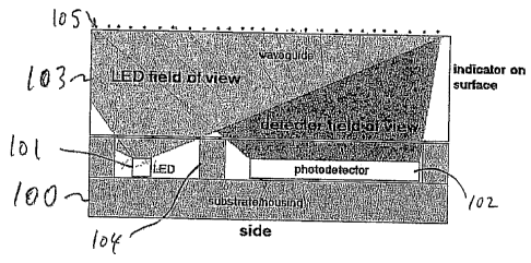
[0009] FIG. 1A is a top view of an optical sensor
device according to one embodiment of the present
invention;
[0010] FIG. 1B is a side view of the optical
sensor device of Fig. 1A;
[0011] FIG. 2A is a side view of the optical
sensor device of FIGs. 1A-1B, illustrating excitation
and indicator response fields of view;
[0012] FIG. 2B is an end view of FIG. 2A;
[0013] FIGs. 3A and 3B are side views illustrating
the problem of emission of light noise from a light
5
CA 02469870 2004-06-09
WO 03/050519 PCT/US02/39675
source of an optical sensor, and the solution achieved
by the present invention, respectively;
[0014] FIG. 4 is a side view illustrating the use
of a curved waveguide surface for an optical sensor
according to an alternate embodiment of the invention;
[0015] FIGs. 5A-5D are side views illustrating the
optimization of waveguide thickness for the sensor
device according to the present invention; and
[0016] FIG. 6 is a graph showing the light
emission profile of an LED light source suitable for
use with the optical sensor device according to the
present invention.
DETAILED DESCRIPTION OF THE PREFERRED EMBODIMENT
[0017] FIGs. 1A and 1B show an embodiment of an
optical sensor device according to the present
invention. The device includes a light source, such as
LED 101, and a light detector, such as photodiode 102,
mounted on a substrate 100. The light source and light
detector are encapsulated by a waveguide 103, the outer
surface of which is provided with a fluorescence-
indicator matrix 105 containing analyte-indicator
molecules. The matrix 105 is disposed on the outer
surface of the waveguide 103 in one of a variety of
different ways, such as by deposition, coating,
adhesion, etc. The light source 101 and light detector
102 are separated from each other by an internal baffle
104a, which is part of a baffle layer portion 104 of
the substrate 100. The baffle portion 104 may be formed
either separately from the substrate 100 or integrally
with formation of the substrate with subsequent etching
or masking of the cavities.
6
CA 02469870 2004-06-09
WO 03/050519 PCT/US02/39675
[0018] Baffle layer 104 can be formed over the
base layer 110 of the substrate 100 to define a number
of cavities into which the light source and
photodetector are placed to be mounted an the
substrate. Prior to forming the waveguide layer 103
over the cavities, the light source cavity is filled
with a transparent epoxy or other polymeric material
106, which preferably has substantially the same
refractive index as the waveguide 103. The fill-in
material 106 may be, but is not required to be, the
same material used for the waveguide 103.
[0019] The photodetector cavity is filled with a
color-doped epoxy or polymeric material 107, which
functions as a filter to block direct or reflected
light from the light source 101 from impinging on the
photodetector 102. The color of the material 107 is
selected to correspond to the peak emission of the
indicator molecules.
[0020] Alternately, the photodetector cavity can
be filled with the color-doped material, and thereafter
the light source cavity can be filled simultaneously
with the formation of the waveguide layer, such that
the light source will be embedded within an integrally
formed waveguide layer.
[0021] Additionally, instead of being filled with
a clear material, the light source cavity also may be
filled with a color-doped material, the color of which
is selected to substantially block all wavelength
emissions from the light source other than the desired,
peak wavelength emission.
[0022] As shown in FIGs. 2A and 2B, the
configuration of the optical sensor device according to
7
CA 02469870 2004-06-09
WO 03/050519 PCT/US02/39675
the invention is based on achieving substantially only
a direct illumination by the light source 101 of
substantially the entire outer surface of the waveguide
103, which is provided with fluorescence indicator
matrix 105, and substantially only a direct collection
on the surface of the photodetector 102 of the
responsive emission from the indicator matrix 105.
Internal baffle 104 prevents stray illumination of the
photodetector 102 by the light source 101. The light
emission profile geometry of the LED light source is
shown in Fig. 6.
[0023] One problem with prior sensor constructs
arises from the fact that the light emitted from
standard LEDs used as light sources is not at a pure
wavelength, but includes a significant amount of light
emission at longer wavelengths, which may reduce the
quality of the measurement signal obtained. For
example, a standard blue LED provides a 460nm
wavelength emission, but because of various factors,
including factors involved in the manufacturing
process, there is a significant amount (e.g.,
approximately 0.1% or more of total emission) of light
emission spreading into the red region (e.g., above
600nm) of the spectrum. The red-doped epoxy material
107 acts as a filter to block the blue wavelengths from
being incident on the photodetector 103, but cannot
filter out such so-called "red-tail" emissions from the
LED light source.
[0024] In the case of an oxygen sensor device
using ruthenium biphenyl phenanthroline as an indicator
matrix, the peak emission of such indicator is 613nm.
Thus, the "red tail" emission of the LED contaminates
8
CA 02469870 2004-06-09
WO 03/050519 PCT/US02/39675
the signal from the indicator. This "red tail"
emission causes the signal baseline to be elevated and
thereby suppresses the useful readable modulation of
fluorescence emission from the indicator. This is
shown in FIG. 3A.
[0025] As shown, blue wavelength light emissions
301 (desired) are accompanied by extraneous, unwanted
red wavelength emissions 302, which can be reflected by
the prior waveguide construct to the detecting surface
of the photodetector 102. According to the direct
illumination construct of the present invention, most
of the unwanted red wavelength emissions 302 from the
LED light source are not reflected at the surface of
the waveguide back to the photodetector, but instead
pass directly out of the waveguide, such that
substantially only red wavelength fluorescence
emissions 303 in response to excitation from the blue
wavelength light waves 301 impinges on the
photodetecting surface of the photodetector 102.
According to experimental measurements, baseline noise
is reduced by more than 40 times the level produced by
the prior geometry (e.g., from 23mV to less than
0.5mV). Additionally, as discussed above, the use of a
blue-doped fill-in material in the light source cavity
can aid in reducing "red-tail" emissions from the light
source.
[0026] The simplest and most efficient
configuration of the optical sensor device according to
the invention is to have a flat surface for the
waveguide, as shown in Figs. 1A-1B, and 2A-2B. It also
is possible to have a curved surface, as shown at in
Fig. 4. Additionally, it is possible to have other
9
CA 02469870 2004-06-09
WO 03/050519 PCT/US02/39675
surface geometries such as a sawtooth, gable, or
inverse surface pattern, in order to increase surface
area and thereby increase the amount of indicator
available for analyte interaction.
[0027] With the prior designs, it was thought that
the curved arc of the waveguide played a role in
focusing of the signal light onto the photodetector.
To the contrary, internal reflectance or focusing are
not significant phenomena according to the design of
the present invention. As shown in Fig. 4, the focal
point 402 of the arc has no relationship to the
detector 102, and in fact is completely outside of the
sensor device altogether.
[0028] Experimental observations and measurements
have confirmed that the predominant amount of indicator
light is produced in response to only direct
illumination from the light source, as opposed to
internally reflected light.
[0029] FIGs. 5A-5D illustrate a number of
different waveguide thickness optimizations in light of
the discovery that reflectance is not a major
contributor to signal strength. As shown, various
waveguide thicknesses were fabricated, where the
thickness is characterized as a proportion of the
distance from the LED light source to the intersection
of the far field emission point X of the LED light
source with the waveguide surface. For each thickness,
signal strength was measured at a fixed LED current and
amplifier gain. As illustrated, for a waveguide
thickness of X/3, a signal of approximately 5mV was
produced; at 2X/3, a signal of approximately 20mV was
produced; at X, a signal of approximately 50mV was
CA 02469870 2004-06-09
WO 03/050519 PCT/US02/39675
produced; and at 4X/3, a signal of approximately 40mV
was produced. From these results, it can be seen that
the peak signal strength is obtained when the thickness
of the waveguide is set equal to X; in other words,
where the far field emission point of the LED light
source coincides with the corner of the waveguide.
This may be achieved by appropriate relative
positioning between the light source and the baffle, by
selection of a light source with a particular
intrinsice emission profile geometry, or by a
combination of these factors.
[0030] Where the surface of the waveguide is made
other than flat in order to obtain an increased surface
area, the thickness X is equal to the mean height of
the surface pattern as measured from the lower surface
of the waveguide.
[0031] The optical sensor device according to the
invention also may be configured as a dual or multi-
detector, with photodetectors mounted on either side of
the LED, and different indicator matrices disposed over
each respective photodetector, such that the same
excitation wavelength of the LED may excite different
fluorescence wavelengths in each indicator matrix.
Alternatively, multiple LEDs may be used, wherein each
LED emits a different excitation wavelength causing a
different fluorescence wavelength response.
[0032] Further, while refractive index matching
has been described according to one preferred
embodiment of the invention, it also is possible to
select different refractive indices for each of the
light source fill-in material, the waveguide material,
and the photodetector fill-in material. It is known
11
CA 02469870 2004-06-09
WO 03/050519 PCT/US02/39675
that light naturally travels from a medium having a
lower refractive index to a medium having a higher
refractive index.
[0033] Accordingly, since it is desired for
excitation light to travel from the light source to the
indicator matrix disposed on the waveguide surface, and
for fluorescence light emission to travel from the
indicator matrix to the photodetector, an alternate
embodiment of the invention would provide successively
higher indices of refraction for the light source fill-
in material, the waveguide material, and the
photodetector fill-in material.
[0034] The invention having been thus described,
it will be apparent to those skilled in the art that
the same may be varied in many ways without departing
from the spirit and scope of the invention. For
example, while the invention has been described with
reference to a fluorescence sensor device for purposes
of illustration, the principles of the invention may be
applied to an optical sensor device using detection
phenomena other than fluorescence. Any and all such
modifications are intended to be encompassed by the
following claims.
12