Note: Descriptions are shown in the official language in which they were submitted.
CA 02469956 2006-02-24
WO 03/056499 PCT/IIS02/41320
CONTACT SMART CARDS HAVING A DOCUMENT CORE,
CONTACTLESS SMART CARDS INCLUDING MULTI-LAYERED
STRUCTURE, PET-BASED IDENTIFICATION DOCUMENT,
AND METHODS OF MAKING SAME
[00011
Technical Field
[0002] The present invention relates generally to identification documents and
smart
cards.
Background and Summary
[00031 Verifying one's true identify is an ever-increasing problem. Identify
theft is
rampant, and stolen id.entifies have even been used to facilitate tenorist
attacks.
Computer networks and secure areas have been breached with misappropriated
keys,
passwords and codes. Conventional solutions typically include a photo
identification
document having a photographic quality image of the license holder on the
document
protected from tampering by one or more security feature. Another solution is
the use
of so-called "smart cards."
[0004] The term "smart card" as used herein is defined broadly to generally
include a
device that carries information. (The definition of a smart card used in this
application
is broad enough to include so-called radio frequency identification cards - or
RFID
cards.). Typically, a smart card includes a microprocessor (or electronic
processing
circuitry) and/or memory circuitry embedded therein. The electronic circuitry
is often
packaged as a module. A memory smart card stores information in electronic
memory
circuits, while a processor smart card can manipulate information stored in
associated
memory. Of course a smart card module can include both processing and memory
CA 02469956 2004-06-11
WO 03/056499 PCT/US02/41320
-2-
circuitry. A "contact" smart card communicates via a physical contact
interface. A
contact smart card is typically inserted into a smart card reader, thereby
making
physical contact between the interface and the reader. A"contactless" smart
card may
have an antenna through which signals are communicated, as shown in U.S.
Patent No.
6,424,029. Thus, a contactless smart card may not need a physical interface.
Of
course, a smart card can include both a contact and contactless (e.g., antenna
and
supporting circuitry) interface. A smart card may be passive in that it lacks
an internal
power source. Power can be supplied through its interface, which energizes the
smart
card's internal circuits. Of course, there are smart cards that may include an
internal
power source. Further background for smart cards and smart card readers can be
found,
e.g., in U.S. Patent Nos. 5,721,781, 5,955,961, 6,000,607, 6,047,888,
6,193,163,
6,199,144, 6,202,932, 6,244,514, 6,247,644, 6,257,486, and 6,485,319.
[0005] Smart cards are capable of performing a variety of functions, including
carrying data, manipulation or processing information and data, controlling
access (e.g.,
by carrying pass codes, biometric data, passwords, etc.), providing
identifying
information, holding biometric data, etc. Of course, this is not an exhaustive
list of
possible smart card functionality.
[0006] A conventional smart card manufacturing process provides a blank card.
The
blank is drilled, perhaps by a second vendor or manufacturer. A smart card
chip is
inserted into a pre-drilled blank. (U.S. Patent No. 6,404,643 discloses a card
with an
integrated circuit. The integrated circuit is attached to a card blank and is
bonded by
melt flowing adhesive. The card blank can have a pre-drilled cavity into which
the
integrated circuit is placed, or may be the same size and shape as is the card
blank and a
space there between is filled with adhesive.) Often times the chip filled
blank is passed
to a third vendor or manufacturer who prints or engraves the chip filled
blank. The
printing processes available at this stage are sometimes limited. In fact,
printing is not
always possible on both sides of the card - due to the contact area presented
by a smart
card module. Even if a smart card is printed after embedding an integrated
circuit
module, the printing may nevertheless be vulnerable to malicious attacks
(e.g., by
changing information printed on the smart card).
CA 02469956 2004-06-11
WO 03/056499 PCT/US02/41320
-3-
[0007] We have found additional limitations that are associated with
conventional
smart cards. In the case of contact smart cards, some of these problems
include the
smart card module popping off the card when flexed, flex stresses that damage
the
smart card module, and/or the card itself cracking with normal wear and tear.
[0008] Accordingly, in one embodiment of the present invention, we provide a
contact smart card including a core layer. The core layer can include a
synthetic paper
- offering flexibility for the contact smart card. Thus, the synthetic paper
core may
also help to reduce cracking often seen after normal wear and tear of
conventional
smart cards. The core layer is preferably preprinted, perhaps with personal
information, prior to the insertion of a smart card module. We can print high
quality
images and text - on both sides of the document, if needed - since the smart
card
module is installed after printing. The print is preferably covered with a
laminate to
offer intrusion protection and wear-and-tear protection. A cavity is formed in
the
laminated structure and integrated circuitry is secured in the cavity.
[0009] Some of our smart card processes can also be controlled by one entity,
if
desired, such as in a"centraP' issue (CI) program. Commercial systems for
issuing ID
documents are of two main types, namely so-called "central" issue (CI), and so-
called
"on-the-spot" or "over-the-counter" (OTC) issue. Of course, we envision that
we will
provide so-called "blank" documents (e.g., document structures without
printing and
lamination, or with some pre-printing and/or some lamination) to over-the-
counter
(OTC) issuing stations.
[0010] Central issue type ID documents are not immediately provided to the
bearer,
but are later issued to the bearer from a central location. For example, in
one type of CI
environment, a bearer reports to a document station where data is collected,
the data is
forwarded to a central location where the card is produced, and the card is
forwarded to
the bearer, often by mail. Another illustrative example of a CI assembling
process
occurs in a setting where a driver passes a driving test, but then receives
her license in
the mail from a CI facility a short time later. Still another illustrative
example of a CI
CA 02469956 2004-06-11
WO 03/056499 PCT/US02/41320
-4-
assembling process occurs in a setting where a driver renews her license by
mail or
over the Internet, then receives a drivers license through the mail.
[0011] Centrally issued identification documents can be produced from
digitally
stored information and generally comprise a core material (also referred to as
"substrate"), such as paper or plastic, sandwiched between a plurality of
layers of, e.g.,
clear plastic laminate, such as polyester or polycarbonate, to protect printed
information
(e.g., photographs, text, barcodes, biometric representations, security
features, etc.)
from wear, exposure to the elements and tampering. The materials used in such
CI
identification documents can offer the ultimate in durability. In addition,
centrally
issued digital identification documents generally offer a higher level of
security than
OTC identification documents because they offer the ability to pre-print the
core of the
central issue document with security features such as "micro-printing", ultra-
violet
security features, security indicia and other features currently unique to
centrally issued
identification documents. Another security advantage with centrally issued
documents
is that the security features and/or secured materials used to make those
features are
centrally located, reducing the chances of loss, misappropriation or theft (as
compared
to having secured materials dispersed over a wide number of "on the spot"
locations).
[0012] In addition, a CI assembling process can be more of a bulk process
facility, in
which many cards are produced in a centralized facility, one after another.
The CI
facility may, for example, process thousands of cards in a continuous manner.
Because
the processing occurs in bulk, CI can have an increase in efficiency as
compared to
some OTC processes, especially those OTC processes that run intermittently.
Thus, CI
processes can sometimes have a lower cost per ID document, if a large volume
of ID
documents is manufactured.
[0013] In contrast to CI identification documents, over-the-counter ("OTC")
identification documents are issued immediately to a bearer who is present at
a
document-issuing station. An OTC assembling process provides an ID document
"on-
the-spot." (An illustrative example of an OTC assembling process is a
Department of
Motor Vehicles ("DMV") setting where a driver's license is issued to a person,
on the
CA 02469956 2004-06-11
WO 03/056499 PCT/US02/41320
-5-
spot, after a successful exam.). In some instances, the very nature of the OTC
assembling process results in small, sometimes compact, printing and card
assemblers
for printing the ID document.
[0014] In identification and security applications, it is often desirable to
increase the
functionality of identification documents. Accordingly, one aspect of the
present
invention may provide the look and/or feel of conventional identification
documents
while providing smart card functionality. In one implementation, we combine an
image
bearing identification card with smart card functionality. We sometimes refer
to these
type of documents as "smart identification documents." In another
implementation,
we "upgrade" an identification document that may have already passed into
circulation
by providing a smart card module within a pre-circulated ID document.
[0015] Another aspect of the present invention involves modification of a
synthetic
paper core-based identification (ID) document to provide a smart card that
includes
integrated circuitry (e.g., a semiconductor chip and interface), laser,
thermal transfer
and/or offset printed images (e.g., including photographic representations)
and/or
customized (or personalized) text and data.
[0016] (In this document, the use of the terms "identification document" and
"ID
document" is intended to include at least all types of ID documents. Note
that, for the
purposes of this disclosure, the terms "document," "card," "badge" and
"documentation" are used interchangeably. In addition, ID documents are
broadly
defined herein and include (but are not limited to), documents, magnetic
disks, credit
cards, bank cards, phone cards, passports, driver's licenses, network access
cards,
employee badges, debit cards, security cards, visas, immigration
documentation,
national ID cards, citizenship cards, social security cards and badges,
certificates,
identification cards or documents, voter registration cards, police ID cards,
border
crossing cards, security clearance badges and cards, gun permits, badges, gift
certificates or cards, membership. cards or badges, tags, CD's, consumer
products,
knobs, keyboards, electronic components, etc., or any other suitable items or
articles
CA 02469956 2004-06-11
WO 03/056499 PCT/US02/41320
-6-
that may record information, images, and/or other data, which may be
associated with a
function and/or an object or other entity to be identified.).
[0017] In addition, in this document, "identification" includes (but is not
limited to)
information, decoration, and any other purpose for which an indicia can be
placed upon
an article in the article's raw, partially prepared, or final state. Also,
instead of ID
documents, our inventive techniques can be employed with product tags, product
packaging, business cards, bags, charts, maps, labels, etc., etc.,
particularly those items
including an laminate or over-laminate structure. The term ID document thus is
broadly defined herein to include these tags, labels, packaging, cards, etc.
[0018] According to another aspect of the present invention, a smart
identification
document includes: a core layer including a first surface and a second
surface; a first
layer of a substantially transparent polymer adjacently arranged on the first
surface of
the core layer; an aperture; and a module. The aperture includes a first
section disposed
in the first polymer layer, the first section including a ledge in the first
polymer layer,
and a second section disposed in at least the core layer. The module includes
electronic
circuitry, wherein at least' a first portion of the module is adjacently
arranged with the
ledge, and at least a section portion of the module extends into at least some
of the
second section of the aperture.
[0019] According to still another aspect of the present invention, an
identification
document includes a core layer including a front side and a back side; printed
indicia
formed on at least the front side of the core layer; a first laminate layer
secured with an
adhesive to the back side of the core layer; a second laminate layer secured
with an
adhesive to the front side of the core layer; a cavity disposed in the first
laminate, the
cavity extending through the first laminate layer, adhesive and into the core
layer; and
electronic circuitry disposed in the cavity.
[0020] According to yet another aspect of the invention, a manufacturing
method
includes the steps of: providing a first laminate and a second laminate, the
first laminate
comprising a front surface and a back surface, and the second laminate
comprising a
CA 02469956 2004-06-11
WO 03/056499 PCT/US02/41320
-7-
front surface and a back surface; adjacently arranging an adhesive with the
back surface
of the first laminate; adjacently arranging an adhesive with the back surface
of the
second laminate; providing a core having a top surface and a bottom surface;
laminating the first laminate, adhesive, core, adhesive and second laminate to
form a
structure; machining a portion of the structure; and providing an integrated
circuitry
module in the machined portion of the structure, the integrated circuitry
module
providing at least some smart card functionality.
[0021] Still another aspect of the present invention relates to a milling tool
for milling
a polymer and a synthetic paper structure to receive a smart card module. The
tool
includes: a fluted shaft having a first section and a second section; a first
cutting edge
having a first bevel disposed on the first section; a second cutting edge
having a second
bevel disposed on the second section, the first and second cutting edges
forming a first
axis; and wherein a non-cutting end of the first bevel and a non-cutting end
the second
bevel form a second axis which is rotated at a first angle in a range of 15-60
degrees
from the first axis.
[0022] Yet another aspect of the present invention relates to a method of
milling a
cavity in an identification document to receive a smart card module. The
identification
document includes at least a laminate layer - document core structure. The
method
includes providing a first cut in the laminate layer to create a rough upper
cavity, the
rough upper cavity including a first aperture; providing a second cut to
create a lower
cavity, the lower cavity extending through the laminate layer into the
document core,
the lower cavity and the rough upper cavity being approximately centered
around a
common axis, wherein the aperture of the lower cavity is relatively smaller
than the
aperture of the rough upper cavity resulting in a shelf in the laminate layer;
and
providing a third cut around the rough upper cavity to create a finished upper
cavity,
the finished upper cavity having an aperture which is larger than the aperture
of the
rough upper cavity, the fmished upper cavity being approximately centered
around the
common axis.
CA 02469956 2004-06-11
WO 03/056499 PCT/US02/41320
-8-
[0023] Still another aspect of the present invention includes an
identification
document including: a first PET (polyethylene terephthalate) film including a
top
surface and a bottom surface; a second PET film including a top surface and a
bottom
surface; an image-receiving layer provided on the first PET film top surface;
and an
adhesive layer in contact with the first PET film bottom surface and the
second PET
film top surface, the adhesive serving to secure the first PET film and the
second PET
film to one another.
[0024] Still another aspect of the present invention provides a method of
making a
contactless smart identification document. The method includes: providing a
carrier
layer including at least an antenna and electronic circuitry, wherein the
carrier
comprises at least one permeable area; arranging the carrier layer between a
first
contact layer and a second contact layer, and then securing the first contact
layer and
second contact layer to the carrier layer through at least one of heat and
pressure so that
at least a portion of one of the first contact layer and the second contact
layer migrates
into the carrier layer at the one permeable area; and providing first and
second laminate
layers over at least the first and second contact layers, respectively.
[0025] Further aspects, features and advantages of the present invention will
become
even more apparent with reference the following detailed description and the
accompanying drawings.
BRIEF DESCRIPTION OF THE DRAWINGS
[0026] FIG. 1 is a cross sectional view of an identification document
including a
document core.
[0027] FIG. 2A is a cross-sectional view of the FIG. 1 document including a
cavity
provided therein to receive a smart card module (e.g., a contact-type smart
card
module).
[0028] FIG. 2B is a cross-sectional view of the FIG. 2A document including
adhesive
provided on a layer shelf.
CA 02469956 2004-06-11
WO 03/056499 PCT/US02/41320
-9-
[0029] FIG. 2C is a cross-sectional view of the FIG. 2A document including a
smart
card module provided in the cavity.
[0030] FIG. 3 is a flow diagram illustrating steps to manufacture, e.g., a
contact-type
smart identification document according to one aspect of the present
invention.
[0031] FIG. 4A is a cross-sectional view of the FIG. 1 document including an
upper
cavity provided in a laminate layer.
[0032] FIG. 4B is a cross-sectional view of the FIG. 4A document including a
lower
cavity extending into a core layer.
[0033] FIG. 4C is a cross-sectional view of the FIG. 4B document including a
finish
cut of the upper cavity.
[0034] FIGS. 5A-5F are diagrams illustrating a milling tool according to one
aspect
of the present invention.
[0035] FIG. 6 is a cross-sectional view of a contactless smart identification
document
according to one implementation.
[0036] FIG. 7 is a cross-sectional view of another implementation of a
contactless
smart identification document.
[0037] FIG. 8 is a cross-sectional view of still another implementation of a
contactless smart identification document.
[0038] FIG. 9 is a cross-sectional view of yet another implementation of a
contactless
smart identification document.
CA 02469956 2004-06-11
WO 03/056499 PCT/US02/41320
-10-
[0039] FIG. 10 is a top view of a contactless smart identification document's
carrier
layer including an antenna and integrated circuitry according to one aspect of
the
present invention.
[0040] FIG. 11 is a cross-sectional view of a contactless smart identification
document according to another implementation of the present invention.
[0041] FIG. 12 is a cross-sectional view of the FIG. 11 contactless smart
identification document including over-laminates.
[0042] FIG. 13 is a cross-sectional view of a finished over-the-counter
identification
document (conventional art).
[0043] FIG. 14 is a cross-sectional view of a PET-based identification
document
according to one implementation.
[0044] FIG. 15 is cross-sectional view of another PET-based document according
to
still another implementation.
[0045] Of course, the drawings are not necessarily presented to scale, with
emphasis
rather being placed upon illustrating the principles of the invention. In the
drawings,
like reference numbers indicate like elements.
DETAILED DESCRIPTION OF THE INVENTION
[0046] The Detailed Description is divided into three sections for the
reader's
convenience (e.g., "Contact Smart Cards Including a Document Core,"
"Contactless
Smart Cards Including Multi-layered Structure," and "Manufacture of PET-Based
Identification Document"). It should be appreciated, however, that elements
and
functionality disclosed in one section can be readily combined with elements
and
CA 02469956 2004-06-11
WO 03/056499 PCT/US02/41320
-11-
functionality found in another section. Therefore, the section headings should
not be
interpreted as limiting the scope of the present invention.
Section 1: Contact Smart Cards Including a Document Core
[0047] For purposes of illustration, the following section will generally
proceed with
reference to contact-type smart cards (which are sometimes interchangeably
referred to
as a "contact smart ID document" or a "smart ID document"). A preferred
contact-
type smart ID document includes a multi-layered ID document including a
document
core and fused or secured polymer laminates. The multi-layered ID document is
provided with integrated circuitry to facilitate processing and/or memory
storage. It
should be appreciated, however, that the present invention is not so limited.
Indeed, as
those skilled in the art will appreciate, the inventive techniques can be
applied to many
other structures formed in many different ways. For example, contactless smart
card
modules can be suitably packaged, with such packages being disposed in a
cavity
created in a multi-layered document structure.
[0048] FIG. 1 is a cross-sectional view of an identification document 1
according to
one aspect of the present invention. The identification (ID) document 1 is
used as the
foundation for a smart ID document. The ID document 1 preferably includes a
core 10,
and a generally transparent laminate 12. The ID document will typically
include a
second laminate layer 14. Adhesive 11 and 13 is preferably used to help adhere
the
laminate layers 12 and 14 to the core 10. (Instead of separate adhesive layers
11 and
13, the laminate 12 may be coated with an adhesive or may include adhesive
materials.)
If indicia (e.g., printed text, images, machine readable code, etc.) is
provided on the
core or laminate surface(s), the adhesive 11 and 13 is preferably transparent.
A
laminate structure can be cut to meet the dimensions specified for a
particular
identification document, if needed.
[0049] Indicia (interchangeably used with "information") can be provided
(e.g.,
screen printed, offset printed, gravure printed, thermal transferred, provided
via ink or
laser jet printing, laser engraved, etc.) on the front and/or back surface of
the core 10 or
CA 02469956 2004-06-11
WO 03/056499 PCT/US02/41320
-12-
laminate 14/adhesive 13 prior to lamination. For example, the information may
include
variable information, which is information that is unique to a cardholder
(e.g., name,
birth date, age, sex, weight, address, biometric information, photograph,
and/or
signature, etc.). The information may also include so-called "fixed"
information.
Fixed information is generally thought of as that information which remains
constant
from card to card, such as issuing agency information, seal, and/or some types
of
security designs, etc. Additional information, e.g., optical variable devices,
can be
provided on the core 10, adhesive 11 and 13, or laminate layers 12 and 14.
(Reference
may be had to assignee's U.S. patent application no. 09/969,200, filed October
2, 2001,
for even further information regarding optical variable inks and devices.).
Other
security features that may be optionally presented on the smart identification
document
include, e.g., ghost images, microprinting, ultraviolet or infrared images,
biometric
information, etc. We can optionally provide a print receiver (e.g., an image-
receiving
layer) to help a core or laminate layer better receive printed or transferred
information.
(For example, see the D2T2 receivers discussed in the present patent document
and in
U.S. Patent No. 6,066,594.).
[0050] Printed or engraved information may optionally include a so-called
digital
watermark. Digital watermarking is a process for modifying physical or
electronic
media to embed machine-readable indicia (or code) into the media. The media
may be
modified such that the embedded code is imperceptible or nearly imperceptible
to the
user, yet may be detected through an automated detection process. In some
embodiments, the printed or engraved information identification document
includes
two or more digital watermarks. In other embodiments, a digital watermark is
"fragile"
in that it is designed to degrade or be lost upon copying and/or reproducing.
[0051] Digital watermarking systems typically have two primary components: an
encoder that embeds the digital watermark in host media, and a decoder that
detects and
reads the embedded digital watermark from a signal suspected of containing a
digital
watermark. The encoder embeds a digital watermark by altering the host media
signal.
(E.g., the encoder can make slight alterations to a graphic, background
pattern or
photograph that is to be printed on an identification document. The
alterations may be
CA 02469956 2004-06-11
WO 03/056499 PCT/US02/41320
-13-
to pixel values, DCT coefficients corresponding to the host media signal,
transform
domain representations of the host media signals, etc., etc.). The reading
component
analyzes a suspect signal to detect whether a digital watermark is present. In
applications where the digital watermark encodes information (e.g., as a
payload or
message bits), the reader extracts this information from the detected digital
watermark.
The reading component can be hosted on a wide variety of tethered or wireless
reader
devices, from conventional PC-connected cameras and computers to fully mobile
readers with built-in displays, etc. By imaging a watermarked surface of an
identification document, the watermark information can be read and decoded by
a
reader.
[0052] Several particular digital watermarking techniques have been developed.
The
reader is presumed to be familiar with the literature in this field. Some
techniques for
embedding and detecting imperceptible watermarks in media signals are detailed
in the
assignee's co-pending U.S. Patent Application No. 09/503,88 1, U.S. Patent No.
6,122,403 and PCT patent application PCT/US02/20832.
[0053] (Material types are now provided by way of example only. Of course,
there
are many other materials that may be suitably interchanged with some aspects
of the
present invention. Returning to FIG. 1, the core 10 material can include a
synthetic
such as TESLIN, other synthetic materials, polymer, composite, and/or
polyolefin, etc.
TESLIN is a synthetic paper sold by PPG Industries, Inc., One PPG Place,
Pittsburgh,
PA 15272 USA. TESLIN can be provided in sheets, with multiple cores taken from
each TESLIN sheet. The laminate (sometimes called an "over laminate") may
include
(but is not limited to) film and sheet products. Laminates usable with at
least some
embodiments of the invention include those which contain substantially
transparent
polymers and/or substantially transparent adhesives, or which have
substantially
transparent polymers and/or substantially transparent adhesives as a part of
their
structure, e.g., as an extruded feature. In some of the embodiments of the
present
invention, the term "laminate" may include both the laminate and adhesive
layers (e.g.,
layers 12 and 11), e.g., in FIGS. 1-2C. Examples of usable laminates include
at least
polyester, polycarbonate, polystyrene, cellulose ester, polyolefin,
polysulfone, or
CA 02469956 2004-06-11
WO 03/056499 PCT/US02/41320
-14-
polyamide, etc. Laminates can be made using either an amorphous or biaxially
oriented polymer as well. A laminate can comprise a plurality of separate
laminate
layers, for example a boundary layer and/or a film layer. Our most preferred
laminate,
however, is a polycarbonate. Various lamination processes are disclosed in
assignee's
U.S. Patent Nos. 5,783,024, 6,007,660, 6066594, and 6,159,327. Other
lamination
processes are disclosed, e.g., in U.S. patent Nos. 6,283,188 and 6,003,581.)
[0054] (The degree of transparency of a laminate can, for example, be dictated
by the
information contained on the core layer, the particular colors and/or security
features
used, etc. The thickness of the laminate layers is not critical, although in
some
embodiments it may be preferred that the thickness of a laminate layer be
about 1-20
mils (where 1 mil is about 25 m). Lamination of any laminate layer(s) to any
other
layer of material (e.g., a core layer) can be accomplished using a
conventional
lamination process, and such processes are well known to those skilled in the
production of articles such as identification documents. Of course, the types
and
structures of the laminates described herein are provided only by way of
example, those
skilled in the art will appreciated that many different types of laminates are
usable in
accordance with the invention. The material(s) from which a laminate is made
may be
transparent, but need not be. Laminates also includes security laminates, such
as a
transparent laminate material with proprietary security technology features
and
processes, which protects documents of value from counterfeiting, data
alteration,
photo substitution, duplication (including color photocopying), and simulation
by use
of materials and technologies that are commonly available. Laminates also can
include
thermosetting materials, such as epoxy.). Suitable laminate materials can be
readily
obtained, e.g., from GE Plastics, headquartered in Pittsfield, MA USA.
Laminates can
be even provided in roll form, e.g., 1000 ft/roll (e.g., about 21 cards/ft).)
[0055] (One adhesive material (e.g., layers 11 and 13 in FIG. 1) can include,
e.g.,
KRTY as provided by Transilwrap, headquartered in Franklin Park, Illinois
60131
USA. The adhesive may also be provided as a laminate layer or coated onto the
laminate or laminate rolls. Other adhesives usable in accordance with some
embodiments of the invention include polyester, polyester urethane, polyether
urethane,
CA 02469956 2004-06-11
WO 03/056499 PCT/US02/41320
-15-
polyolefin, and/or hot melt or ultraviolet or thermally cured adhesive,
thermoplastics,
etc. The multi-layered structure is formed during a lamination process, in
which
adjustments to the processing time, temperature and pressure can be varied to
optimize
lamination.)
[0056] Dimensions of an ID document will vary according to specified design
requirements. For example, applicable International Organization for
Standardization
(ISO) specifications for identification documents may specify required
dimensions.
Within specified dimensions there is some dimension play. In one
implementation, we
provide a core including an 4-20 mil depth, adhesives with a 2-7 mil depth,
and
laminate layers ranging from 3-15 mils. Our most preferred implementation
provides a
12 mil back laminate, a 2 mil back adhesive, a 12 mil core, a 2 mil front
adhesive and a
mil front laminate.
[0057] In some implementations we provide a matte finish on a top surface of
the
back laminate layer. The matte finish helps to feed the laminate layer if
provided in
roll form. The matte finish may also provide a tactile security feature, as an
inspector
can feel the texture of the card (e.g., a matted finish) to determine if the
card is
legitimate.
[0058] With reference to FIG. 2A, a cavity or well 20 is provided (e.g.,
machined,
milled, cut or laser etched, etc.) in the FIG. 1 ID document 1. We
interchangeably use
the terms "cavity" and "well" in this document. The well 20 provides a housing
or
receptacle for a smart card integrated circuit module (hereafter sometimes
referred to a
"module" or as "smart card module"). The shape and dimensions of the well 20
will
vary according to the shape and dimensions of a selected smart card module
that is to
be inserted into the well 20. For discussion purposes we have chosen to
illustrate the
present invention with respect to the Hitachi AE 45C smart card chip module,
as
provided by Hitachi, located in Maidenhead, Berkshire, UK, and which provides
32K
bytes of memory. A multi-application chip operating system, e.g., MLTLTOS or
any
other suitable chip operating system, can be used to control the operation of
the smart
card module. MULTOS can be obtained, e.g., through Moasco, Ltd in London,
CA 02469956 2004-06-11
WO 03/056499 PCT/US02/41320
-16-
England. (We note that dimensions of the Hitachi AE 45C module are analogous
to the
Atmel 1608 Module, which, like other smart card modules, can be suitably
interchanged with the Hitachi AE 45C module.). Our chip selection will
naturally
dictate some of the shapes and dimensions discussed below. It should be
appreciated,
however, that the present- invention is not so limited. Indeed, some aspects
of the
present invention anticipate the cooperation with may different smart card
modules, and
corresponding cavity 20 shapes and depths. For example, in one implementation,
instead of the rectangular shaped cavity 20 as illustrated in FIG. 2A, we
provide an oval
shaped cavity. The oval shaped cavity cooperates, e.g., with an oval shaped
smart card
module (e.g., Atmel's model no. AT88SC1608-090T-00 - headquartered in San
Jose,
CA USA). Of course there are many other cavity and module shapes and sizes
that will
fall within the scope of the present invention.
[0059] Returning to FIG. 2A, cavity 20 may include an upper chamber (or
cavity) 20a
and a lower chamber (or cavity) 20b. The depth D of the upper chamber 20a is
generally dependent on a corresponding depth of the smart card module. We have
found that it is generally preferable to seat the smart card module in the
cavity 20 so
that the module's interface is about flush with the outer surface of laminate
12,
although the module's contact interface can slightly protrude above (or below)
the
laminate 12 surface. This seating arrangement helps to prevent the smart card
module
from catching on objects, which may undesirably unseat the module from the
cavity 20.
The upper chamber 20a, which is adjacently arranged to the lower chamber 20b,
preferably includes a relatively larger aperture than that of the lower
chamber 20b. The
aperture differences between the lower cavity 20b and the upper cavity 20a
results in a
shelf 22. We have found that it is preferably (but not required) to provide
the shelf 22
in the laminate layer 12, while allowing sufficient laminate shelf depth d,
since a smart
card module's adhesion (e.g., via adhesive) to the laminate layer 12 is
generally
superior than a module's adhesion (e.g., via adhesive) to adhesive layer 11 or
core layer
10. If the depth d is too small, the shelf 22 may pull up and away from the
adhesive 11
and/or core 10 layers. In some cases we have found that too small of a depth d
results
in the shelf 22 and adhesive 11 together pulling up and away from the core 10.
The
CA 02469956 2004-06-11
WO 03/056499 PCT/US02/41320
-17-
depth d in our most preferred implementation is about 2 mils. Of course this
preferred
depth d may vary as structure layer depths or module dimensions vary.
[0060] If using the ID document 1 as shown in FIG. 1, the lower cavity 20b
preferably extends through, e.g., the laminate 12 and adhesive 10, and into
the core 10.
A depth D+ of the lower cavity 20b is generally dependent on the vertical
depth of the
smart card module. While not necessary to practice the present invention, we
can
provide enough depth D+ so that the bottom of the smart card module will
"float" in
the well or otherwise not contact the bottom B of the well 20 when the ID card
is at rest
(see FIG. 2C). This floating arrangement provides somewhat of a cushion for
the smart
card module - allowing the card to flex without causing undue stress on the
bottom of
the smart card module. (We note that some thought should be given to the depth
D+ of
a well, since if the well is too deep, a card assembler risks having the
bottom surface of
the smart card module show through the remaining core depth - resulting in
unwanted
discoloration when viewed from the front of the card.) In our most preferred
implementation, the D+ depth extends about 10 mils into the core layer. (Of
course,
this depth can be altered according to layer dimensions and smart card module
used,
etc.). In other implementations, the bottom and/or sides of a smart card
module contact
the bottom B and/or or sides, respectively, of the well 20, perhaps through an
adhesive.
[0061] We preferably provide an adhesive to help secure a smart card module 26
in
the cavity 20. There are several options for providing adhesive. With
reference to FIG.
2B, we can provide an adhesive 24 directly onto shelf 22, e.g., through
injection or spot
adhesives. Alternatively, the smart card module can be coated with an adhesive
on a
side that is to be adjacently positioned with shelf 22. (We note that a smart
ID
document manufacturing method can be automated. In such cases, the smart card
modules can be provided in roll form, e.g., one reel including about 7,500
chips.
Adhesive (e.g., cyanoacrylate epoxy from Henkel of America, in Gulph Mills,
Pennsylvania USA) or a roll of glue tape (e.g., Tesa HAF 8410 HS or Tesa BDF
8410
from Tesa Tape, Inc. in Charlotte, NC USA) can be applied to the bottom side
of the
chip roll. Assembling machines provided by, e.g., Muhlbauer, headquartered in
Roding, Germany, can be used for final assembly. Such an automated process may
CA 02469956 2004-06-11
WO 03/056499 PCT/US02/41320
-1 ~-
proceed by printing a card, laminating, cutting and verifying dimensions and
printed
information, and then milling, implanting a smart card module and then
encoding or
initializing the smart card module. Testing can be performed to detect a bad
smart card
module, etc.). In an implementation without shelf 22, we coat the sides and/or
bottom
of a smart card module with adhesive, and/or provide adhesive to a cavity and
then
insert the module.
[0062] A smart ID document results once the integrated circuitry module is
secured in
a cavity of an ID document (FIG. 2C). A smart card module can be optionally
programmed to store relevant information such as information printed on the
document,
biometric information, account information, cryptographic hashes or other
algorithmic
representation of data, passwords, etc. One programmer example is a
computerized
smart card Personalizer, e.g., as provided by Muhlbauer of Germany, which
enters
commands or data into the smart card module. Other programmers are provided,
e.g.,
from Hitachi and Atmel, among many others. Information stored in the smart
card
circuitry is optionally cross-correlated with information printed on the smart
card. This
cross-correlation can be checked to verify authenticity of the document or
stored
information. Or if a digital watermark is provided on the document, a
watermark
payload can be cross-correlated with information stored in the smart card's
memory
circuitry. A cross-correlation of the watermark information and the module's
stored
information can be analyzed to determine authenticity of the identification
document.
[0063] FIG. 3 is a flow diagram illustrating the steps to manufacture a
contact smart
card according to one implementation. A document core or substrate is provided
(step
S30). The document substrate (or sometimes a laminate/adhesive layer) is
printed (step
S32), e.g., to include personalized or variable information. If printing on an
inner
laminate or adhesive layer, the printing may be reversed so it appears
properly oriented
when viewed from the outer surface of the laminate or adhesive layer. The
printing
may also include security patterns and designs, digital watermarks, and may
also
include optical variable devices, such as those provided with optical variable
ink. A
photograph may be included in the variable information. Printing options are
widespread and may include, e.g., offset printing, screen printing, laser or
ink jet
CA 02469956 2004-06-11
WO 03/056499 PCT/US02/41320
-19-
printing, laser engraving, thermal transfer, etc. An image receiving layer can
also be
used, e.g., to better facilitate the reception of the information. The printed
substrate is
preferably laminated (step 34). The lamination process may involve adhesives
or
adhesive layers, but the present invention is not so limited. The laminate
structure
optionally may be cut to desired specifications (step not shown), if needed. A
cavity or
well is provided in the laminated, printed core (step S36). The cavity can be
machined,
milled, drilled, cut, etched (laser or chemical), etc. The cavity is
preferably sized to
accommodate a corresponding smart card module. In some implementations, the
cavity
extends into the core. The corresponding smart card module is secured in the
cavity
(step S38). While this method is anticipated to be most suited for contact-
type smart
card, we anticipate that some contactless-type smart card modules can be
packaged
such that they may also be provided in a cavity, e.g., as created with
reference to FIGS.
2A-3.
Milling Operation (Example)
[0064] FIGS. 4A-4C are cross sectional diagrams illustrating the methodology
behind
one milling implementation of the present invention. A cavity is milled to
receive a
smart card module. We note that the illustrated method is but one of many
methods
that can be used to mill or machine out a cavity in an ID document.
[0065] We start our milling discussion by returning to FIG. 1. FIG. 1
illustrates a
multi-layered identification document including a core and laminates. We
realized that
the material used for the laminate (e.g., polycarbonates) and core (e.g., a
synthetic like
TESLIN) was susceptible to tearing or leaving burrs when cut. The illustrated
milling
technique (FIGS. 4A-4C) optimizes a milling operation to eliminate burrs in
the multi-
material cavity so that a smart card module can be securely mounted therein.
6
[0066] A milling (or machining or etching) tool contacts the back laminate 12
and
machines a rough upper cavity 20a (see "Rough Cut" represented with dotted
lines in
FIG. 4A). The machining tool then (preferably after re-centering or realigning
according to a reference or start position, or common axis) contacts the
laminate at the
bottom of the rough upper cavity to machine out the lower cavity 20b (see FIG.
4B).
CA 02469956 2004-06-11
WO 03/056499 PCT/US02/41320
-20-
We then pass the machining tool back through the upper cavity (preferably
after re-
centering or realigning according to a reference or start position, or common
axis) to
shave or finish the upper cavity (see FIG. 4C). FIG. 4C illustrate the finish
cut in
relation to the original rough cut (dotted lines). An advantage of the finish
pass is to
clean up any rough edges or burrs left from the rough cut. The finish pass can
be
subtle, e.g., slightly expanding the upper cavity 20a while cleaning up debris
and rough
edges. (In our preferred implementation, the fmish pass comprises about a.001
mil
cut.) Table 1, below, illustrates software code that can be used to automate
such a
milling process. The code is written so as to operate a Muhlbauer cutting
station, e.g.,
through a user interface (e.g., a text editor or graphical user interface)
such as provided
by Galil Motion Control, Inc. (Muhlbauer is headquartered in Roding, Germany,
while
Galil Motion Control, Inc. is headquartered in Rocklin, CA USA.). Of course,
the
dimensions and instructions as illustrated in the Table 1 software code can be
changed
according to need, card dimensions, module dimensions, card materials used,
cutting
station and interface, etc.
Table 1
#F30 ! Program Name !
CRADIUS =1.8
POSX=15.1 !Defines center position for cavity on card !
POSY=23.89
POSZ=0.0
JS #MOVXYZ
POSZ=0.18 1 Surface ruff cut - LEAVE .0015" FOR Finish
cut!
POS1Z=0.18
LENGTHX=12.9 ! LEAVE about .010" FOR CLEAN-UP
WIDTHY=11.6 ! !
RADIUS=2.3
JS#RECT ! Milling Instruction
PR, -6000 ! Re-center over cavity !
BGY
AMY
POSZ=0.47 ! Lower Cavity final cut !
POS1Z=0.47
LENGTHX=8.4
CA 02469956 2004-06-11
WO 03/056499 PCT/US02/41320
-21-
WIDTHY=8.7
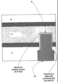
RADIUS=1.8
JS #RECT ! Milling Instruction
PR ,-5000 ! Re-center for finish cut
BGY
AMY
POSZ=0.21 ! Finish Cut
POS1Z=0.21
LENGTH=13.4
WIDTHY=12.1
RADIUS=2.3
JS #RECT ! Milling Instruction
POSX=15.1 ! Return Tool to a home position
POSY=23.89
POSZ=0.0
JS #WAITPOS
END
[0067] In an alternative implementation, we make a rough cut for the lower
cavity
20b, and then follow-up with finish cut for the lower cavity 20b. In other
implementations, we make one cut for the upper cavity 20a, and one cut for the
lower
cavity 20b. In still further implementations, we provide a first cavity
including the
lower cavity 20b, and then expand the first cavity to includes the final upper
cavity 20a.
Debris can be evacuated from the cavity 20 through pressurized air or
vacuuming, etc.
Milling Tool (Example)
[0068] FIG. 5A-5D are diagrams of a milling tool that can be used to mill a
cavity in
an ID document. It should be appreciated that this is but one of many tools
that can be
used to provide a cavity in an identification document. In some cases, a laser
or
chemical process is used to create a cavity. In other implementations,
conventional
tools or cutters are used to machine or cut a cavity in an identification
document.. It
will also be appreciated that while specific dimensions (in millimeters) are
provided in
the FIG. 5 representations, the present invention is not so limited. Indeed
the
dimensions can be changed in many respects without deviating from the scope of
this
aspect of the present invention.
CA 02469956 2004-06-11
WO 03/056499 PCT/US02/41320
-22-
[00691 With reference to FIGS. 5A and 5B, the cutting tool 50 preferably
includes a
shaft 51 having a first 52 and second 54 section. The shaft 51 can be fluted
as shown in
the figures. The first section 52 includes a first cutting edge 52a and the
second section
54 includes a second cutting edge 54a. Each of the cutting edges 52a and 54a
can be
off-centered (see OCI and OC2 in FIG. 5A). Off-centering the cutting edges
helps to
provide an aggressive cutting tool, e.g., by increasing the tool's angle of
attack (e.g.,
the angle at which a cutting edge encounters material to cut). A face (or
surface) of
each of the first and second cutting edges 52a and 54a is preferably beveled
or tapered.
The taper helps to ensure that the cutting edge is optimally presented to the
document
material. While the FIG. 5 representations may suggest a 15-degree bevel, we
anticipate acceptable cuts with a tool including a bevel in a range of about 5-
35
degrees. As shown in FIGS. 5A and 5B, a relief 56 can be provided for each of
the
cutting edges. The relief is another mechanism to help present the cutting
edge to the
material in a favorable manner. While the figures suggest a 45-degree relief,
we
anticipate that a relief in the range of about 30-60 degrees will provide
acceptable
results.
[0070] One advantage of this type of tool is that its configuration allows for
a carving
type cutting motion, in comparison to conventional tools that provide more of
a
scrapping or tearing motion. A carving motion allows for a clean cut, e.g.,
for shelf 22.
A clean shelf allows for a better bonding surface with an adhesive.
[0071] Other features and advantages of this cutting tool are readily
discemable from
further examination of the drawings, including FIGS. 5C-5F.
Inventive Combinations
[0072] In addition to the inventive aspects detailed above and in the claims,
some of
the inventive combinations with respect to (e.g., contact-type) smart ID
documents
include the following:
[0073] A. An identification document comprising:
a core layer including a front side and a back side;
CA 02469956 2004-06-11
WO 03/056499 PCT/US02/41320
-23-
printed indicia formed on at least the front side of the core layer;
a first laminate layer secured with an adhesive to the back side of the core
layer;
a second laminate layer secured with an adhesive to the front side of the core
layer;
a cavity disposed in the first laminate, the cavity extending through the
first
laminate layer, adhesive and into the core layer; and
electronic circuitry disposed in the cavity.
[0074] Al. The identification document of combination A wherein the cavity
comprises an upper cavity and a lower cavity, an aperture of the upper cavity
being
relatively larger than an aperture of the lower cavity so as to result in a
shelf, wherein
the electronic circuitry is packaged and a portion of the package is
adjacently arranged
on the shelf.
[0075] A2. The identification document of combination Al, wherein a portion of
the
package floats in the lower cavity.
[0076] A3. The identification document of combination Al, wherein the lower
cavity
includes a floor in the core layer, and wherein a portion of the package
extends into the
lower cavity but does not contact the floor when the identification document
is at rest.
[0077] B. A manufacturing method comprising the steps of
providing a first laminate and a second laminate, the first laminate
comprising a
front surface and a back surface, and the second laminate comprising a front
surface
and a back surface;
adjacently arranging an adhesive with the back surface of the first laminate;
adjacently arranging an adhesive with the back surface of the second laminate;
providing a core having top surface and a bottom surface;
laminating the first laminate, adhesive, core, adhesive and second laminate to
form a structure;
machining a portion of the structure; and
CA 02469956 2004-06-11
WO 03/056499 PCT/US02/41320
-24-
providing an integrated circuitry module in the machined portion of the
structure, the integrated circuitry module providing at least some smart card
functionality.
[0078] B 1. The method of combination B, further comprising a step of printing
the
core prior to said laminating step.
[0079] B2. The method of combination B1, wherein the printing comprises at
least
one of a photograph, name, birth date, social security number, signature and
identification number.
[0080] B3. The method of combination B1, wherein the printing comprises at
least
one of: offset inks, process inks, thermal transfer, laser xerography and
laser printer
toners.
[0081] B4. The method of combination B1, further comprising the step of
cutting the
structure into the shape of an identification card.
[0082] B5. The method of combination B, wherein the core comprises a sheet of
TESLIN.
[0083] B6. The method of combination B, wherein the at least some smart card
functionality comprises at least one of data carrier, data manipulation,
access control,
identification verification, biometric carrier and data processing.
[0084] B7. The method of combination B1, wherein the printing comprises
steganographic indicia.
[0085] B8. The method of combination B7, wherein the steganographic indicia
comprises a digital watermark.
[0086] B9. The method of combination B8, wherein the digital watermark
comprises
CA 02469956 2004-06-11
WO 03/056499 PCT/US02/41320
-25-
a fragile watermark.
[0087] B10. The method of combination B8, wherein the integrated circuitry
module
comprises information stored therein, and wherein the information corresponds
to the
digital watermark for cross-correlation.
[0088] B 11. An identification document made according to any one of the
combinations set forth in B - B 10.
[0089] C. A manufacturing method comprising the steps of:
providing a first laminate and a second laminate, the first laminate
comprising a
front surface and a back surface, and the second laminate comprising a front
surface
and a back surface;
providing a core having top surface and a bottom surface;
laminating the first laminate, second laminate and core to form a structure,
the
structure comprising the back surface of the first laminate in contact with
the top
surface of the core and the back surface of the second laminate in contact
with the
bottom surface of the core;
milling a cavity through the first laminate and into the core for affixing an
integrated circuitry module; and
providing an integrated circuitry module in the cavity, the integrated
circuitry
module providing at least some smart card functionality.
[0090] Cl. The method of combination C, further comprising the step of
printing the
core or second laminate prior to said laminating step.
[0091] C2. The method of combination C, wherein the core comprises a silica-
filled
polyolefin.
[0092] C3. The method of combination C, wherein the core comprises a synthetic
paper.
CA 02469956 2004-06-11
WO 03/056499 PCT/US02/41320
-26-
[0093] C4. The method of combination C, wherein each of the first laminate and
second laminate comprise an adhesive layer, the adhesive layers being arranged
between the first laminate and the core and second laminate and the core,
respectively.
[0094] C5. The method of combination C4, wherein the adhesive comprises a
thermoplastic adhesive.
[0095] C6. The method of combination C, wherein at least one of the first
laminate
and the second laminate comprises a security feature.
[0096] C7. An identification document made according to combination C. '
[0097] C8. An identification document made according to combination C4.
[0098] C9. The method of combination C, wherein said milling step creates a
shelf in
the first laminate layer, and wherein said providing an integrated circuitry
module in
the cavity step provides the module to be adjacently arranged on the shelf.
[0099] C10. The method of combination C9, wherein at least a portion of the
module
extends into the core layer.
[0100] C11. The method of combination C10, wherein the module portion that
extends into the core layer does not extend to a bottom of the cavity.
[0101] D. A manufacturing method comprising the steps of:
providing a first laminate and a second laminate, the first laminate
comprising a
front surface and a back surface, and the second laminate comprising a front
surface
and a back surface;
coating the back surface of the first laminate with adhesive;
coating the back surface of the second laminate with adhesive;
providing a core having top surface and a bottom surface;
CA 02469956 2004-06-11
WO 03/056499 PCT/US02/41320
-27-
laminating the first laminate, second laminate and core to form a structure,
the
structure comprising the adhesively coated back surface of the first laminate
in contact
with the top surface of the core and the adhesively coated back surface of the
second
laminate in contact with the bottom surface of the core;
machining a portion of the structure; and
providing an integrated circuitry module in the machined portion of the
structure, the integrated circuitry module providing at least some smart card
fu.nctionality.
[0102] Dl. A document made according to the method of combination D.
[0103] E. A manufacturing method comprising the steps of:
providing a first laminate and a second laminate, the first laminate
comprising a
front surface and a back surface, and the second laminate comprising a front
surface
and a back surface;
providing a core having top surface and a bottom surface;
laminating the first laminate, second laminate and core to form a structure,
the
structure comprising the back surface of the first laminate in contact with
the top
surface of the core and the back surface of the second laminate in contact
with the
bottom surface of the core; and
providing an integrated circuitry module in the structure, the integrated
circuitry
module providing at least some smart card functionality.
[0104] E1. A document made according to the method of combination E.
[0105] F. A method of milling a cavity in an identification document to
receive a
smart card module, the identification document comprising at least a laminate
layer -
document core sandwich structure, said method comprising:
providing a first cut in the laminate layer to create a rough upper cavity,
the
rough upper cavity including a first aperture;
providing a second cut to create a lower cavity, the lower cavity extending
through the laminate layer into the document core, the lower cavity and the
rough upper
CA 02469956 2004-06-11
WO 03/056499 PCT/US02/41320
-28-
cavity being approximately centered around a common axis, wherein the aperture
of the
lower cavity is relatively smaller than the aperture of the rough upper cavity
resulting in
a shelf in the laminate layer; and
providing a third cut around the rough upper cavity to create a finished upper
cavity, the finished upper cavity having an aperture which is larger than the
aperture of
the rough upper cavity, the finished upper cavity being approximately centered
on the
common axis.
[0106] Fl. The method of combination F, wherein the laminate layer comprises
an
adhesive, so that the sandwich structure comprises a laminate - adhesive -
document
core structure.
[0107] F2. The method of combination Fl, wherein the shelf is provided in
laminate.
[010$] F3. The method of combination F2, wherein the document comprises
document-holder specific printing thereon.
[0109] F4. The method of combination F, wherein the laminate layer comprises a
polymer and the document core comprises a synthetic paper.
[0110] F5. The method of combination F4, wherein the synthetic paper comprises
TESLIN.
[0111] F6. An identification document made according to any one of the
metliods set
forth in combinations F - F5.
[0112] G. A contact smart card comprising:
a core layer including a top surface and a back surface;
a first laminate layer adjacently secured to the top surface core layer;
a second laminate layer adjacently secured to back surface of the core layer;
printed indicia provided either on the top surface of the core layer or on a
surface
CA 02469956 2004-06-11
WO 03/056499 PCT/US02/41320
-29-
of the first laminate layer that is to be secured to the top surface of the
core, the indicia
comprising at least some information that is unique to a bearer of the contact
smart
card;
a well disposed in at least the second laminate layer; and
an integrated circuitry module provided in the well, the module including a
contact surface.
[0113] Gl. The contact smart card of combination G, wherein the well includes
a
shelf in the laminate layer and the well extends into the core layer, and
wherein at least
a first portion of the module is adjacently arranged on the shelf and a second
portion of
the module extends into the core layer.
[0114] G2. The contact smart card of combination G wherein the information
comprises a photographic representation of the bearer.
[0115] H. A milling tool for milling a polymer and a synthetic paper structure
for
receiving a smart card module comprising:
a fluted shaft having a first section and a second section;
a first cutting edge having a first bevel disposed on the first section;
a second cutting edge having a second bevel disposed on the second section,
the
first and second cutting edges forming a first axis; and
wherein a non-cutting end of the first bevel and a non-cutting end the second
bevel form a second axis which is rotated at a first angle in a range of 15-60
degrees
from the first axis.
[0116] H1. The milling tool of combination H, wherein the first bevel is
tapered in a
range of 5 and 45 degrees.
[0117] H2. The milling tool of combination H, wherein the first bevel is
tapered at an
angle of 15 degrees.
CA 02469956 2004-06-11
WO 03/056499 PCT/US02/41320
-30-
[0118] H3. The milling tool of combination H, wherein the second bevel is
tapered in
a range of 5 and 45 degrees.
[0119] H4. The milling tool of combination H3, wherein the second bevel is
tapered
at an angle of 15 degrees.
[0120] H5. The milling tool of combination H3 wherein the first angle
comprises 45
degrees.
Section 2: Contactiess Smart Cards including
Multi-layered Structure
[0121] The following section primarily focuses on contactless smart cards.
However,
it should be appreciated that our inventive techniques can be extended to
include
contact smart card and other identification documents as well. A contactless
smart card
can be generalized as a card including integrated electronic circuitry. Unlike
a contact-
type smart card, where the integrated electronic circuitry communicates via a
physical
contact interface, a contactless smart card communicates (e.g.,
transfers/receives) data
via an antenna or transceiver structure. The antenna (or transceiver) is
connected to the
integrated circuitry. A contactless smart card may include an internal power
source to
energize its electronic circuitry. Alternatively, the integrated circuitry can
be energized
through electromagnetic energy received through the antenna (or other
transceiver
structure). The integrated circuitry can include data processing circuitry for
processing
or manipulating data or software instructions, andlor memory circuitry for
data storage.
(Of course, the circuitry can include other components such as a clock
generator,
system bus structure, and buffers, etc., etc.).
[0122] Some contactless smart cards have heretofore been affiliated with their
fare
share of problems. One problem is protecting a contact between the antenna and
the
integrated circuitry. Communication ability of a contactless smart card will
be lost or
hampered if the contact between an antenna and circuitry is severed.
Protecting this
CA 02469956 2004-06-11
WO 03/056499 PCT/US02/41320
-31-
connection becomes a chore, since smart cards are often subjected to onerous
stresses
and flexing. An associated problem with conventional smart cards is longevity.
We
have found that conventional contactless smart cards crack, degrade, and/or
fail to
operate as anticipated. We overcome some or all of these drawbacks in one
implementation of an inventive contactless smart card.
[0123] Another implementation of contactless smart cards combines a
contactless
smart card with the benefits of an identification document. Some
identification
document benefits may include (but are not limited to): photographic
representations,
personalized information, security indicia, over-laminate layers, etc., etc.
[0124] In another implementation of a contactless smart card, we provide a
multi-
layered card structure that provides the benefits of a smart card with the
durability and
flexibility of a multi-layer structure. Multi-layers may also provide
protection from
unwanted radiation, e.g., ultraviolet radiation, which may interfere with
contactless
communication.
[0125] In yet another implementation of a contactless smart card, we employ a
central
issue (CI) type issuing model when producing inventive contactless smart
cards. A
central issue model allows us to tightly control the materials and processing
of
contactless smart cards.
[0126] These and further features, implementations and advantages of our
contactless
smart cards (or "contactless smart ID documents") will become even more
evident with
reference to the following disclosure and corresponding figures.
[0127] One implementation of a multi-layer contactless smart card 60 (or smart
ID
document) is disclosed with reference to FIG. 6. A carrier layer 61 is
provided. The
carrier layer 61 carries or includes a contactless smart card module, such as
an antenna
100 (or transceiver, etc.), and electronic circuitry 102 (see FIG. 10). The
circuitry 102
may include processing and memory circuitry (e.g., 2K-256K bytes, etc.). In
some
cases a chip operating system is employed with the integrated circuitry 102.
The
CA 02469956 2004-06-11
WO 03/056499 PCT/US02/41320
-32-
antenna communicates with the circuitry 102 through an interface or contact
104.
(Note that there may be more or less contacts as shown in FIG. 10.). Of
course, the
antenna 100 can include a plurality of receiving elements (e.g., loops or
coils, copper
wiring, etc.).
[0128] The carrier 61 is sandwiched between contact layers 62a and 62b.
Contact
layers 62a and 62b may include, e.g., a polymer, synthetic, composite, etc.,
and can
include a layered structure such as a polymer-adhesive layering. The carrier
layer 61 is
preferably permeable, e.g., like a mesh or scrim. The carrier layer 61
material can be
composed of many different materials including, e.g., polymers, PET
(polyethylene
terephthalate), PET fibers, polycarbonate, polyester, poly-composite,
polystyrene,
cellulose ester, polyolefin, polysulfone, poly-bends, composites, etc., etc.
One suitable
scrim material that includes contactless smart card circuitry and transceiver
means is
provided by Hitachi Semiconductor (America), Inc., with US headquarters in San
Jose,
CA. (For example, Hitachi can provide a scrim inlay, in sheet sizes of about
15 3/4"x24",
including 6-by-6 wired antennas and corresponding integrated circuits, each
antenna/circuit/carrier layer have a dimension of about 45mmx77mm. When using
scrim sheets, and/or when aligning individual antenna/circuitry, some care
should be
given to ensure proper alignment of the carrier layer 61 (e.g., including the
antenna/circuitry) when considering cutting (e.g., die cutting), preprint
information
and/or personalization of a contactless smart identification document. If
using a mesh
material, we have found excellent results when using a mesh weight-per-area
ratio in a
range of about 5 grams/ma - 20 grams/m2. Our most preferred mesh includes a
ratio of
about 10 grams/m2. In some implementations the antenna 100 and integrated
circuitry
102 are positioned or embedded between two sheets of carrier (e.g., scrim or
mesh)
material. Of course, there are many other acceptable carrier layers and/or
contactless
smart card modules that are suitably interchangeable with this aspect of the
present
invention such as those provided by Philips and Sony, among many others.
[0129] A permeable carrier 61 facilitates the migration of contact layers 62a
and 62b
into and/or through the carrier layer 61 during a lamination (e.g., heat
and/or pressure)
process. The migration of the contact layers into and/or through the carrier
61 helps to
CA 02469956 2004-06-11
WO 03/056499 PCT/US02/41320
-33-
firmly secure the smart card module, including the contact 104 between the
antenna
100 and integrated electronic circuitry 102.
[0130] In an alternative implementation we embed (e.g., through injection
molding,
lamination, etc.) a contactless smart card module in a carrier layer 61. The
carrier layer
61 is generally solid instead of permeable in this implementation. In this
implementation the carrier layer 61 preferably includes a material that is
receptive to
lamination or bonding, e.g., a polymer or adhesive material. In still a
further alternative
implementation, a carrier layer 61 comprises a metal or conductive material
(e.g.,
copper wiring). The carrier layer 61 itself serves as the antenna 100, which
is
connected to the electronic circuitry 102 via a contact 104.
[0131] Regardless of which implementation is employed, contact layer 62a
and/or
62b can receive indicia (or printing) provided thereon. The printing may
include
information that is typically associated with an identification document, such
as a
photographic representation of the card bearer, variable information, e.g.,
name,
address, sex, height, weight, biometric information, signature, and/or
citizenship, etc.,
etc. The printing may optionally include so-called fixed information such as
information pertaining to an issuing authority, security feature (e.g.,
optical variable
devices, etc.), etc. In other implementations, the indicia includes a digital
watermark.
Instead of printing information on the contact layer 62a or 62b surface, we
sometimes
print information on an underside of an laminate/adhesive (e.g., 64a and/or
64b). If
printing on an inner laminate or adhesive layer, the printing may be reversed
so it
appears properly oriented when viewed from an outer surface of the laminate or
adhesive layer. In some implementations, the ink and printing techniques
disclosed in
Bentley Bloomberg and Bob Jones' patent application titled "INK WITH COHESIVE
FAILURE AND IDENTIFICATION DOCUMENT INCLUDING SAME," filed
concurrently herewith (Attorney Docket No. P0714D), will be used to print a
contactless (or contact) smart identification document. Printing techniques
may include
offset, gravure, screen, thermal transfer, ink or laser jet, etc.
CA 02469956 2004-06-11
WO 03/056499 PCT/US02/41320
-34-
[01321 In some implementations of our contactless smart ID document, we pre-
print
information onto a layer surface. The pre-printed information may include
variable or
fixed information.
[0133] Generally transparent laminate layers 64a and 64b are provided over the
contact layers 62a and 62b, respectively. The laminate layers 64a and 64b are
secured
to the contact layers, e.g., through a conventional lamination process
involving heat
and/or pressure. Laminates like those discussed above in Section 1 can be used
here
also. Laminate layers 64a and 64b provide some degree of intrusion protection
for
information printed on the smart card, as well as providing additional
strength and a
moisture barrier.
[0134] While specific dimensions may be dictated according to identification
document required standards, we note that our preferred dimensions for the
contactless
smart identification document shown in FIG. 7 include: carrier (3-15 mils);
contact
layers (3-16 mils); and laminate (2-15 mils). A preferred range of document
depths is
between about 27-40 mils, with our most preferred document depth includes
about 30
mils.
[0135] Further implementations and examples of contactless smart
identification
documents are discussed with reference to FIGS. 7-12.
[0136] With reference to FIG. 7, contact layers 62a and 62b include an
adhesive
(AD)/polymer/adhesive (AD) structure. The adhesive can be coated or layered on
the
polymer. The polymer layers (62a and 62b) may be formed from any polymer, for
example polyester, polystyrene, cellulose ester, polyolefin, polysulfone, or
polyimide.
Either an amorphous or biaxially oriented polymer may be used. But we use
polycarbonate as our most preferred polymer. The polymer 62a and 62b can be
colored, e.g., white, to help accentuate indicia provided thereon or on the
laminate
layers 64a or 64b. (In some implementations (not shown), we even provide a
synthetic
with adhesive layers (e.g., adhesively coated TESLIN), composite, poly-bend
and/or
paper -- instead of a polymer -- as a contact layer 62a and 62b material.).
The contact
CA 02469956 2004-06-11
WO 03/056499 PCT/US02/41320
-35-
layers 62a and 62b can optionally include coloration, e.g., white, if desired.
The
adhesive layers AD (or coating) help secure the contact layers 62a and 62b to
the
carrier layer 61 and to the laminate layers 64a and 64b during a lamination
process. In
one implementation the adhesive comprises a co-extruded polyurethane (PU)
(e.g., with
a soft point between about 230-290 F.). In another implementation we use an
aliphatic
PU-based adhesive, CLA-93A, from Thermedics, Inc. in Wobum, MA. Still another
suitable adhesive is KRTY as provided by Transilwrap, headquartered in
Franklin Park,
Illinois 60131 USA. Other suitable adhesives may include polyester, polyester
urethane, polyether urethane, polyolefin, poly-composites, thermoplastic
adhesives,
and/or a hot melt or ultraviolet or thermally cured adhesive; of course, an
adhesive may
be coated, extruded or cast on to one surface of the polymer layer. The
laminate layers
64a and 64b can also include, e.g., a polymer, polycarbonate, polyester,
polyester
urethane, poly-composite, polystyrene, polybutylene terephthalate (PBT),
cellulose
ester, polyolefin, polysulfone, polyimide, and/or polybutylene terephthalate
(PBT), etc.
Here again, our most preferred laminate layers 64a and 64b each comprise
polycarbonate. Polycarbonate sheets are widely available, e.g., from GE
Plastics,
headquartered in Pittsfield, MA.
[0137] With reference to FIG. 8, contact layers 62a and 62b preferably include
an
Adhesive (AD2)/Polymer/Adhesive (AD 1) structure, while the laminates (64a and
64b)
preferably include a Polymer/Adhesive (AD3) structure. Adhesive 2 is selected
so as to
provide a favorable bond with Adhesive 1 and Adhesive 3. Similarly, Adhesive 1
is
selected to favorably bond with adhesive 2 and 3. (In some cases, Adhesive 2
and
Adhesive 3 will comprise the same adhesive.). Our most preferred
implementation
employs a polycarbonate as the polymer and polyurethane as the adhesives. Of
course,
other materials as discussed above can be used instead. If the adhesive layers
include
polyurethane, and since the foundation of polyurethane chemistry is generally
based on
isocyanate, a variety of monomers and different reactions can be exploited for
synthesis
of polymeric materials with desired properties, such as flexibility,
toughness, durability,
adhesion, and UV-stability by other additives. Additional polyurethane
compounds
need not be explored herein; rather, one inventive concept is applying
different
polyurethane compounds to the various layers to achieve desired properties.
CA 02469956 2004-06-11
WO 03/056499 PCT/US02/41320
-36-
[0138] With reference to FIG. 9, our contact layers 62a and 62b and our
laminate
layers 64a and 64b each comprise a polymer (or synthetic)/adhesive structure.
The
adhesive sides (or coating) contact one another to help form a bond. Our most
preferred implementation employs a polycarbonate as the polymer and a
polyurethane
as the adhesive. Of course, other materials as discussed in this patent
document and
those known in the art as suitable equivalents can be used instead.
[0139] With reference to FIG. 11, we provide yet another example of a
contactless
smart identification document. We start with scrim inlay sheets (e.g., with a
sheet size
of about 15 3/4' x 24" that include about 6 x 6 antenna 100/chip 102
structures, with
each antenna/chip structure having a dimension of about 45mm x 77mm, as can be
supplied from HITACHI). Of course the scrim inlay sheets can be cut or
otherwise
sized as well. The antenna/chip structure is preferably disposed between (or
embedded) two scrim layers or sheets to form a scrim core 110.
[0140] The scrim core 110 is preferably sandwiched between contact layers 112
and
114. Each contact layer 112 and 114 preferably includes a polycarbonate layer
(a) and
polyurethane layers (b and c) (e.g., each layer comprises about 2 mils of
polyurethane
(e.g., CLA93A from Thermedics, Inc.), about 8 mils of white polycarbonate film
(e.g.,
as supplied by GE Plastics), and about 2 mils of polyurethane (e.g., CLA93A)).
The
polyurethane layers (b and c) can be coated, extruded, sprayed, layered, etc.
onto the
polycarbonate layer (a). Some care is given to the alignment of the scrim 110
(e.g.,
including multiple antenna/chip structures) and contact layers 112 and 114 to
allow for
favorable printing and cutting down stream. In some situations, we can even
provide a
registration marker (e.g., printing) on an outer surface of the polycarbonate
or
polyurethane to help properly align the contact layers 112 and 114. In other
cases we
provide information (e.g., so-called fixed indicia) on an outer surface of
layer 112b and
114c. The information can be offset printed, xerographically printed, laser
printed,
gravure printed, etc., etc.
CA 02469956 2004-06-11
WO 03/056499 PCT/US02/41320
-37-
[0141] Contact layers 112 and 114 are secured to the scrim core 110. For
example,
we
attach the contact layers 112 and 114 through a lamination process (e.g., a
heated
surface,
roller, or iron press). The H1 structure shown in FIG. 11 results (i.e.,
without the
spacing as illustrated). A preferred resulting structure is an 8.5" x 11"
sheet, including
a laminated scrim core 110/contact layer 112 and 114 structure. Of course,
other sheet
sizes can be used as well. If using an 8.5" x 11" sheet there are usually
about nine
antenna/chip structures per sheet. We have two preferred branches in our
process at
this point. A first branch includes cutting (e.g., die cutting) the sheet into
blanks after
the Hl structure is assembled. Each blank includes one antenna/chip structure
having a
cross-section as shown in FIG. 11. The blanks can be, e.g., supplied to an
over-the-
counter issuing station, and further processed by, for example, printing
personal
information on the blank or on an over-laminate and/or programming the on-card
chip.
[0142] The second branch, perhaps better suited for use with a central-issue
model, is
discussed with reference to FIG. 12. The Hl structure sheet (e.g., including
multiple
antenna/chip structures) is even further protected by providing over-laminate
sheets
116a and 11 6b (e.g., 7 mil clear polycarbonate, e.g., HP92W supplied from GE
Plastics). In some cases, the over-laminates 11 6a and 11 6b will include an
adhesive
(not shown) to even further help the lamination process. The laminate layers
116a and
116b are preferably personalized prior to lamination. The personalization may
include
printing variable information (e.g., photographs, text, graphics, signatures,
etc., etc.)
through laser printing (e.g., Xerox's DOC12 laser printer), ink jet printing,
offset
printing, screen-printing, etc. (We note that the printing of variable
information is
preferably reversely printed in the FIG. 12 implementation, since the print is
provided
on an inner surface of the laminate layers 116a and/or 116b. Thus, the printed
information appears correctly aligned when viewed from the "view angle" shown
in
FIG. 12.).
[0143] The over-laminates 116a and 116b can be secured to the H1 structure
through,
e.g., lamination. One lamination techniques is a platen press, which receives
the H1
CA 02469956 2004-06-11
WO 03/056499 PCT/US02/41320
-38-
structure and over-laminates 11 6a and 11 6b. The platen press includes upper
and lower
plates (e.g., Teflon coated metal or glass plates), which press (e.g., about
2.5K PSI) the
H1 structure and over-laminates 116a and 116b with heat (e.g., up to about 275
F) to
form the H2 structure (i.e., without the spacing as illustrated). The
lamination time
varies between about 3-15 minutes, with an optimal lamination of about 10
minutes.
Of course, other lamination techniques (e.g., rollers, press, pads, etc.) can
be used to
secure the over-laminates 11 6a and 11 6b to the H1 structure. The laminated
structure
H2 is cut (e.g., die cut) to yield multi-contactless smart identification
documents. Each
of these contactless smart identification document can be programmed as needed
(e.g.,
the on-board chip 102 can be programmed to include personalized information
such as
pass codes, biometric information, identification information, information
corresponding to the cardholder or to information printed on the
identification
document, etc.).
[0144] VWhile specific structures have been discussed with respect to FIGS. 6-
12, we
note that many other implementations will fall within the scope of the present
invention. For example, additional layers (e.g., laminate layers or print
layers) can be
added to the illustrated structures. Also, in a few cases, we use a structure
including a
contact layer/carrier/contact layer structure, or a laminate/contact
layer/carrier/contact
layer structure. In another inzplementation, we provide a cavity in an
identification
document, and then secure a contactless smart card module in the cavity.
[0145] And while we have described certain materials and dimensions for our
contactless smart identification documents the present invention should not be
limited
to such. Indeed, the present invention includes many more contactless smart
identification documents of different dimensions and materials.
Inventive Combinations
[0146] In addition to the inventive aspects detailed above and in the claims,
some of
the inventive combinations with respect to (e.g., contactless) smart lD
documents
include the following:
CA 02469956 2004-06-11
WO 03/056499 PCT/US02/41320
-39-
[0147] A. A method of manufacturing a contactless smart card comprising the
steps
of:
providing a first contact layer and a second contact layer, the first contact
layer
comprising a front surface and a back surface, and the second contact layer
comprising
a front surface and a back surface;
providing an adhesive adjacently with at least the back surface of the first
contact layer;
providing an adhesive adjacently with at least the back surface of the second
contact layer;
providing a carrier having a top surface and a bottom surface;
combining the first contact layer, second contact layer and carrier to form a
multi-layered structure, wherein the carrier comprises an antenna and
electronic
circuitry therein.
[0148] Al. The method of combination A, wherein the carrier comprises scrim
and
the electronic circuitry provides at least some smart card functionality.
[0149] A2. The method of combination Al, further comprising the steps of:
coating at least the front surface of the first layer; and
coating at least the front surface of the second layer.
[0150] A3. The method of combination A2, wherein the coating comprises
polyurethane, and the first and second layers each comprises polycarbonate.
[0151] A4. The method of combination A3, further comprising the step of
laminating
a top laminate and a bottom laminate respectively so as to be in contact with
the front
surface of the first contact layer and the front surface of the second contact
layer.
[0152] A5. The method of combination Al, further comprising the step of
printing at
least the first contact layer prior to said combining step.
CA 02469956 2004-06-11
WO 03/056499 PCT/US02/41320
-40-
[0153] A6. The method of combination Al, further comprising providing a
laminate
over at least the first contact layer, wherein the laminate comprises
personalized
information thereon, the information being document-holder specific.
[0154] B. A method of producing smart cards or identification documents
comprising the steps of:
providing a scrim core comprising electrical circuitry and an antenna; and
providing the scrirn core between a first layer and a second layer so that the
first
layer and second layer migrate into or through the scrim layer.
[0155] B 1. The method of combination B, wherein the first layer and second
layer
each comprise polycarbonate.
[0156] B2. The method of claim B 1, wherein the first layer contacts a core
top side
and the second layer contacts a core bottom side, wherein the top side layer
is coated
with a first polyurethane material and the bottom side second material is
coated with a
second polyurethane material.
[0157] B3. The method of any one of claims B, B1 and B2, wherein the
electrical
circuitry operates to provide at least some smart card functionality.
[0158] B4. The method of claim B3, wherein the at least some smart card
functionality comprises at least one of data carrier, data manipulation,
access control,
identification verification, biometric carrier and data processing.
[0159] C. A smart identification document manufactured by the method in any
one
of
claims A-A6 and B-B4.
[0160] D. A method of making a contactless smart identification document
comprising:
CA 02469956 2004-06-11
WO 03/056499 PCT/US02/41320
-41-
providing a carrier layer including at least a transceiver and electronic
circuitry,
wherein the carrier comprises at least one permeable area;
arranging the carrier layer between a first contact layer and a second contact
layer, and then securing the first contact layer and second contact layer to
the carrier
layer through at least one of heat and pressure so that at least a portion of
one of the
first contact layer and the second contact layer migrates into the carrier
layer at the one
permeable area; and
providing a first laminate layer over at least the first contact layer.
[0161] D1. The method of combination D, wherein indicia is provided on at
least
one of the first contact layer and the first laminate layer prior to said
providing a first
laminate layer step.
[0162] D2. The method of combination Dl further comprising providing a second
laminate layer over the second contact layer.
[0163] D3. The method of combination Dl wherein the first contact layer and
the
first laminate layer each comprise a polymer.
[0164] D4. The method of combination D3, wherein the first contact layer
comprises an adhesive/polymer/adhesive structure.
[0165] D5. The method of combination D4 wherein the second contact layer
comprises an adhesive/polymer/adhesive structure.
[0166] D6. The method of combination D3, wherein the first laminate comprises
a
polymer/adhesive structure..
[0167] D7. The method according to any one of combinations D3-D6, wherein the
polymer comprises polycarbonate.
CA 02469956 2004-06-11
WO 03/056499 PCT/US02/41320
-42-
[0168] D8. The method according to combination D7 wherein the adhesive
comprises polyurethane.
[0169] E. A contactless smart identification document comprising:
a first contact layer;
a second contact layer;
a carrier layer sandwiched in between the first and second contact layers, the
carrier layer including at least a transceiver and electronic circuitry;
wherein at least a portion of the first contact layer and the second contact
layer
have migrated into the carrier layer, the migration helping to secure at least
a portion of
the transceiver or electronic circuitry to the first and second contact
layers; and
a first laminate layer covering the first contact layer and a second laminate
layer
covering the second contact layer.
[0170] El. The contactless smart identification document of combination E
wherein
the carrier comprises at least one of a scrim and mesh.
[0171] F. A method of manufacturing a contactless smart card comprising the
steps
of:
providing a first layer and a second layer, the first layer comprising a front
surface and a back surface, and the second layer comprising a front surface
and a back
surface;
coating at least the back surface of the first layer with an adhesive;
coating at least the back surface of the second layer with an adhesive;
providing a core having a top surface and a bottom surface;
combining the first layer, second layer and core to form a core structure, the
core structure comprising the coated back surface of the first layer in
contact with the
top surface of the core and the coated back surface of the second layer in
contact with
the bottom surface of the core, wherein the core comprises an antenna and
electronic
circuitry contained therein.
CA 02469956 2004-06-11
WO 03/056499 PCT/US02/41320
-43-
[0172] G. A method of producing smart identification documents comprising the
steps of:
providing a scrim core comprising electrical circuitry and an antenna; and
providing the scrim core between a first layer and a second layer.
Section 3: Manufacture of PET-Based Identification Document
[0173] The following section focuses primarily on identification documents. In
particular, we present an incredibly earth-friendly and easily recycle-able
identification
document at a relatively low cost-per card. In one implementation, we provide
an
identification document structure including PET (polyethylene terephthalate)
materials.
PET material also has good strength and flexibility (with a low cracking
tendency) and
high anti-abrasion properties - while also providing advantageous cost
efficiencies.
[0174] We envision that in some implementations of the present invention, our
inventive a PET-base identification documents will be used in an over-the-
counter
(OTC) issuing model. As discussed in the background section above, over-the-
counter
("OTC") identification documents are generally issued immediately to a bearer
who is
present at a document-issuing station. An OTC assembling process provides an
ID
document "on-the-spot". (An illustrative example of an OTC assembling process
is a
Deparhnent of Motor Vehicles ("DMV") setting where a driver's license is
issued to a
person, on the spot, after a successful exam.). In some instances, the very
nature of the
OTC assembling process results in small, sometimes compact, printing and card
assemblers for printing the ID document. Of course, our inventive PET
identification
documents can be used in a central issue (CI) model as well.
[0175] One example of an OTC identification document (as disclosed in our U.S.
Patent No. 6,066,594) is shown in FIG. 13. FIG. 13 shows a schematic cross-
section
through an over-the-counter identification document (card). The document
comprises a
core layer 112 formed of an opaque white reflective polyolefin (e.g., a TESLIN
sheet)
and printed on both surfaces with fixed indicia 114.
CA 02469956 2004-06-11
WO 03/056499 PCT/US02/41320
-44-
[01761 The printed core layer 112 is sandwiched between two polymer layers 116
formed from an amorphous or biaxially oriented polyester or other optically
clear
plastic such as polycarbonate. Each of these polymer layers 116 is fixedly
secured to
the core layer 112 by a layer 118 of adhesive. On the opposed side of each
polymer
layer 116 from the core 112 is provided an image-receiving layer 120 suited to
the
acceptance of printed image or portrait or other variable indicia (indicated
schematically at 122) by dye diffusion thermal transfer methods. The material
used to
form the image-receiving layers 120 is chosen so as to be immiscible with the
polymer
system of the donor sheet used, in accordance with U.S. Patent No. 5,334,573.
[0177] With reference to FIG. 14, we present an inventive over-the-counter
identification document including PET materials. In contrast to the FIG. 13
document,
the FIG. 14 implementation is a coreless structure. The document primarily
includes
two PET layers (or films). Transilwrap, of Franklin Park, IL, provides a
suitable
polyethylene terephthalate (PET) film under the trade name "TXP. " In some
implementations we provide an amorphous PET fihu or layer. Of course, there
are
many other PET films that can be suitably interchanged with this aspect of
present
invention. The two PET layers are combined, e.g., through a conventional
lamination
process. As shown in FIG. 12 we can use adhesive layers (e.g., thermoplastic
adhesives - preferably PET-based adhesives) to help secure the PET layers. The
adhesive layers can be coated or layered with the PET layers. A resulting
structure PET
structure is cut into required identification document sized cards, if needed.
(We note
that the document's height H can be adjusted according to required
identification
document specifications. For example, the PET layers are preferably between
about 5-
15 mils and the adhesive layers are preferably between about 2-10 mils. One
implementation comprises 10 mil PET layers (e.g., Transilwrap's TXP white PET
film) and 5 mil adhesive layers (e.g., Transilwrap's KRTY (polyolefin)).
[0178] The outer surface of a PET layer preferably receives information or
indicia
provided thereon. The PET layer can include coloration, e.g., white to even
better
accentuate the indicia. The information can include, e.g., variable
information such as
CA 02469956 2004-06-11
WO 03/056499 PCT/US02/41320
-45-
a cardholder's name, address, photograph, signature, biometric information,
etc. and/or
fixed information (e.g., infonnation which is common to a number of cards,
such as the
issuing authority, security features, etc.). The printing may also include a
so-called
digital watermark. The watermark may be embedded in a background tint or
pattern, a
graphic or photograph, etc. A watermark can also be embedded through text or
font
manipulation as well. While we preferably transfer information to the PET
layer
through a dye diffusion thermal transfer -- or "D2T2" -- process, the PET
layer can
also be offset printed, ink or laser jet printed, laser etched, etc. We
provide information
on an outer surface of both PET layers in some implementations. We can also
print
information in stages. For example, we can pre-print fixed information on a
PET layer
or PET substrate prior to lamination (or after lamination) and before a second
stage
printing of variable information. The information can also include a
registration or
calibration marker to help align the identification document in subsequent
printing
steps.
[0179] The PET layer can be can be adapted to even better receive printed
information. For example, we can provide a receiving-layer or "image receiving-
layer"
on an outer surface of a PET film. The term "image" in this disclosure should
be
understood to include all forms of printed and transferred information
including
images, graphics, text, machine readable code, and/or designs, etc., etc. The
image-
receiving layer (e.g., about a 2-20 micron layer) may be formed from any
material
capable of receiving an image, e.g., by dye diffusion thermal transfer. (In
some cases
we use Transilwrap's DITX receiving fluid as an image-receiving layer. In
other cases,
a polymer (e.g., PVC) is used to form an image-receiving layer is first
dissolved in an
organic solvent, such as methyl ethyl ketone, dichloromethane or chloroform,
and the
resultant solution is coated onto the PET layer using conventional coating
apparatus,
and the solvent is then evaporated to form the image-receiving layer. However,
if
desired, the receiving layer can be applied to the PET layer by extrusion
casting, or by
slot, gravure or other known coating methods. Of course, other materials and
receiving
layers, e.g., such as those disclosed in U.S. Patent Nos. 5,334,573 and
6,066,594, may
be suitable interchanged with this image-receiving aspect of the present
invention.
CA 02469956 2004-06-11
WO 03/056499 PCT/US02/41320
-46-
[0180] It may be advantageous to coat the image-receiving material at a
centralized
production facility and then provide resultant "blank" documents to a
plurality of
document issue stations (OTC stations) at which variable data is applied to
the image-
receiving layers of the identification documents.
[0181] Following the printing of information on an image-receiving layer (if
provided, otherwise after printing on the PET layer), a protective layer (not
shown) is
optionally affixed over at least a portion of the image-receiving layer. The
protective
layer serves to protect the relatively fragile image-receiving layer from
damage, and
also prevents bleeding of information (e.g., thermal transfer dye) from the
image-
receiving layer. Materials suitable for forming such protective layers are
known to
those skilled in the art of dye diffusion thermal transfer printing and any of
the
conventional materials may be used provided that they have sufficient
transparency and
sufficient adhesion to the specific image-receiving layer with which they are
in contact
and/or block bleeding of dye from this layer. However, in keeping with the
theme of
this aspect of the present invention, we preferably apply a transparent PET-
based
protective laminate, if used.
[0182] The protective layer may optionally provide additional security and/or
features
for the identification document. For example, the protective layer may include
a low
cohesivity polymeric layer, an optically variable ink, variable information,
an image
printed in an ink which is readable in the infra-red or ultraviolet but is
invisible in
normal white light, an image printed in a fluorescent or phosphorescent ink,
cohesive
failure ink, or any other available security feature which protects the
document against
tampering or counterfeiting, and which does not compromise the ability of the
protective layer to protect the identification document against wear and the
elements.
[0183] With reference to FIG. 15 we provide yet another alternative
implementation
of a PET-based identification document. In particular, we provide a PET
substrate,
protected by PET protective laminates. Of course we can use adhesives to help
secure
the PET laminates to the PET substrate. The PET substrate is preferably
colored, e.g., a
white opaque color. Prior to lamination we provide information (e.g., variable
and/or
CA 02469956 2004-06-11
WO 03/056499 PCT/US02/41320
-47-
fixed information) on an outer surface or surfaces of the PET substrate. The
PET
substrate (or PET laminate) can be coated, prior to lamination, with an image-
receiving
material as discussed above. The image-receiving material can be provided
between
the PET laminate and PET substrate (e.g., on either or both of these layers).
The
image-receiving material can be alternatively (or in addition to) provided on
an outer
surface of the PET laminate layer. If information is provided on an outer-
surface of a
PET laminate, a thin film protective coat or layer can be optionally provided
over the
information for enhanced protection. A completed structure can be sized
according to
need (e.g., height H). Our structure, however, preferably includes dimensions
in the
following ranges: PET substrate (5-25 mils); PET laminates (2-15 mils) and
adhesive
layers, if used (2-8 mils).
[0184] From the foregoing, it will be seen that our PET-based identification
documents provides an over-the-counter identification document that affords
significant
improvements in durability (e.g., flexibility and crack-resistance) and earth-
friendly
characteristics (e.g., recycle and low-hazardous emissions during production)
as
compared with the other OTC identification documents. These types of PET-based
ID
documents can also be provided at a significantly lower cost than other OTC
(and CI)
documents. Our PET-based identification documents can also provide a durable
and
secure identification document that is instantly produced over-the-counter. It
should be
appreciated that our PET-base identification document can also include so-
called
"blanks," or document structures without printing, or with printing but prior
to
personalizing the document.
[0185] While we prefer that our. PET identification documents include all PET
materials, it should be appreciated that our inventive PET-based ID documents
need not
be limited as necessarily including all PET. For example, a polymer (but non-
PET)
over-laminate may be added, a non-PET adhesive may be used, a non-PET image
receiving layer is employed, etc. And of course the dyes or inks and other
security
features will not generally be PET-based. Such deviations certainly fall
within the
scope of this aspect of the present invention.
CA 02469956 2004-06-11
WO 03/056499 PCT/US02/41320
-48-
Inventive Combinations
[0186] In addition to the inventive aspects detailed above and in the claims,
some of
the inventive combinations with respect to PET-based ID documents include the
following:
[0187] A. A coreless identification document comprising:
a first PET (polyethylene terephthalate) film including a top surface and a
bottom surface;
a second PET film including a top surface and a bottom surface;
an image-receiving layer provided on the first PET film top surface; and
an adhesive layer in contact with the first PET film bottom surface and the
second PET film top surface, the adhesive serving to secure the first PET film
and the
second PET film to one another.
[0188] Al. The document of combination A, wherein the receiving layer
comprises a
layer capable of being imaged by dye diffusion thermal transfer.
[0189] A2. The document of combination A wherein the image-receiving layer
comprises a layer capable of being imaged by gravure printing.
[0190] A3. The document of combination A, wherein the image-receiving layer
comprises a depth in a range of 2 to 15 microns.
[0191] A4. The document of combination A, wherein the first PET film and the
second PET film each comprises a depth of about 10 mils.
[0192] A5. The document of combination A, wherein the adhesive layer comprises
at
least two adhesive layers.
[0193] A6. The document of combination A, wherein the adhesive comprises PET.
CA 02469956 2004-06-11
WO 03/056499 PCT/US02/41320
-49-
[01941 A7. The document of combination A, wherein indicia is provided on the
image-receiving layer.
[0195] A8. The document of combination A7, wherein a laminate layer is
provided
over the indicia on the image-receiving layer.
[0196] A9. The document of combination A7, wherein the indicia is provided
through dye diffusion thermal transfer (D2T2).
[0197] A10. The document of combination A7, wherein the indicia is provided
through gravure printing.
[0198] Al 1. The document of combination A, further comprising a second image-
receiving layer provided on the second PET film top surface.
[0199] A12. The document of combination Al l, wherein indicia is provided on
the
second image-receiving layer.
[0200] A13. The document of combination A12, wherein a laminate layer is
provided over the indicia on the second image-receiving layer.
[0201] A14. The document of any one of combinations A7 and A13, wherein the
indicia comprises at least one of a digital watermark and information that is
specific to
one who will bear the document.
[0202] A15. The document of combination A, wherein each of the first and
second
PET layers comprises white coloration.
[0203] A16. The document of combination A15, wherein each of the first and
second
PET layers comprises substantially amorphous PET.
[0204] B. An identification document comprising:
CA 02469956 2004-06-11
WO 03/056499 PCT/US02/41320
-50-
a PET (polyethylene terephthalate) core layer comprising a first surface and a
second surface,
a first layer of a substantially transparent PET fixed to the first surface of
the
PET
core layer;
a second layer of a substantially transparent PET fixed to the second surface
of
the PET core layer; and
at least one image-receiving layer capable of being receiving information, the
image-receiving layer being fixed to at least one of the first transparent PET
layer and
the first surface of the PET core layer.
[0205] B1. The document of combination B, wherein the receiving layer
comprises a
layer capable of being imaged by dye diffusion thermal transfer.
[0206] B2. The document of combination B wherein the image-receiving layer
comprises a layer capable of being imaged by gravure printing.
[0207] C. An identification document comprising:
a first PET (polyethylene terephthalate) film including a top surface and a
bottom surface;
a second PET film including a top surface and a bottom surface; and
an adhesive layer in contact with the first PET film bottom surface and the
second PET film top surface, the adhesive serving to secure the first PET film
and the
second PET film to one another.
[0208] D. A method of making an identification document comprising the steps
of:
providing a first PET (polyethylene terephthalate) film including a top
surface
and a bottom surface;
providing a second PET fihn including a top surface and a bottom surface;
providing an image-receiving layer adjacently arranged on the first PET film
top surface; and
CA 02469956 2004-06-11
WO 03/056499 PCT/US02/41320
-51-
providing an adhesive layer so as to be in contact with the first PET film
bottom
surface and the second PET film top surface, the adhesive serving to secure
the first
PET film to the second PET film.
[0209] D. A method of making an identification document comprising the steps
of:
providing a PET (polyethylene terephthalate) core layer comprising a first
surface
and a second surface,
providing a first layer of a substantially transparent PET so as to be
adjacently
arranged with the first surface of the PET core layer;
providing a second layer of a substantially transparent PET so as to be
adjacently
arranged with the second surface of the PET core layer; and
providing at least one image-receiving layer capable of being receiving
information, the image-receiving layer being adjacently arranged with at least
one of
the first transparent PET layer and the first surface of the PET core layer.
Conclusion
[0210] Having described and illustrated the principles of the technology with
reference to specific implementations, it will be recognized that the
technology can be
implemented in many other, different, forms.
[00211] For example, while we have described a contact-type smart card module
as
including, e.g., a Hitachi AE 45C module, the present invention is not so
limited.
Indeed many other smart card modules are contemplated, e.g., Atmel's 1608,
ModuleEight, and products from Philips, EVM, etc., etc. Of course other
modules can
be used to facilitate similar/additional smart card functionality. A cavity
can be formed
to accommodate the various shapes and dimensions of alternative smart card
modules.
[0212] In at least one embodiment (not shown), laminate layers are formed into
a
pouch into which the core layer slips. With a pouch, methods such as heat,
pressure,
CA 02469956 2004-06-11
WO 03/056499 PCT/US02/41320
-52-
adhesives, and the like, are usable to bond the core layer to the pouch
laminates. Those
skilled in the art will appreciate that many known structures and
configurations for
laminating are usable with the invention.
[0213] While we use terms herein like "front" and "back," these terms are
provided
primarily for the reader's convenience. For example, a smart card module can
be
provided on a "front" side, instead of a"back" side as discussed in section 1.
[0214] The technology disclosed herein can be used in combination with other
technologies. Examples include the technology detailed in the following
applications:
09/747,735 (filed 12/22/00); 09/969,200 (filed 10/2/01) and U.S. Provisional
Application No. 60/429,115 (filed 11/25/02). Also, instead of ID documents,
the
inventive techniques can be employed with product tags, product packaging,
business
cards, smart cards, bags, charts, maps, labels, etc., etc. The term ID
document is
broadly defined herein to include these tags, labels, packaging, cards, etc.
[0215] While many features and aspects of the present invention have been
disclosed
herein, it will be appreciated that not all aspects and features need be
incorporated into
each of the following claims.
[0216] The particular combinations of elements and features in the above-
detailed
embodiments are exemplary only; the interchanging and substitution of these
teachings
with other teachings in this and the above-identified patent documents are
also
expressly contemplated.
[0217] The technology disclosed herein can be used in combination with other
technologies. For example, instead of traditional smart cards, the inventive
techniques
can be employed with identification documents, drivers' licenses, passports,
product
tags, product packaging, business cards, bags, charts, maps, labels, etc. The
terms
"smart card" and "smart ID document" are broadly defined herein to include
such
licenses, passports, tags, labels, packaging, cards, etc.
CA 02469956 2004-06-11
WO 03/056499 PCT/US02/41320
-53-
[0218] It should be appreciated that while specific dimensions and components
have
been presented herein (including the drawings), the present invention is not
limited to
such dimensions and specific components. Indeed, many of the document
dimensions,
materials, printing techniques and smart card circuitry can be interchanged
without
deviating from the scope of the present invention.
[0219] In view of the wide variety of embodiments to which the principles and
features discussed above can be applied, it should be apparent that the
detailed
embodiments are illustrative only and should not be taken as limiting the
scope of the
invention. Rather, we claim as our invention all such modifications as may
come
within the scope and spirit of the following claims and equivalents thereof.