Note: Descriptions are shown in the official language in which they were submitted.
CA 02470095 2004-06-11
WO 03/052838 PCT/US02/39846
1
LIGHT-EMITTING DIODE WITH PLANAR OMNI-DIRECTIONAL REFLECTOR
TECHNICAL FIELD
[0001] The present invention relates generally to a light-emitting diode (LED)
and, more particularly, to an LED with an omni-directional reflector for
enhanced light
extraction efficiency.
BACKGROUND OF THE INVENTION
[0002] LEDs emit light in one or more of the infrared, visible, and
ultraviolet
spectral regions when an electrical current is passed through a
semiconducting, light-
emitting region. As shown in Fig. 1, a common LED 1 emits light in the 550 nm -
700
nm wavelength range. LED 1 comprises an aluminum gallium indium phosphide
(AlGaInP) active region 2 lattice-matched to a gallium arsenide (GaAs)
substrate 3.
Active region 2 comprises a light-emitting region 4 surrounded by two
oppositely doped
confinement layers 5. LED 1 may be referred to as an absorbing-substrate light-
emitting diode (AS-LED) due to the light-absorbing characteristic of the GaAs
substrate
3. The chemical formula for the composition of the active region material is
(Al Ga1_x)0.5Ino,5P, where x can vary between 0.0 and 1Ø This chemical
composition
ensures that the (AlxGa1_x)o.5Ino.5P, commonly abbreviated as AlGaInP, is
lattice-
matched to the GaAs substrate 3.
[0003] Typically, AS-LED 1 comprises a window 6 overlying active region 2.
Window 6 may be composed of gallium phosphide (GaP) that may also contain
small
amounts of other elements such as Al and In. Window 6 may also be composed of
aluminum gallium arsenide, or AIxGa1_XAs, commonly abbreviated as AlGaAs. An
optically opaque top contact 9, typically comprising a highly electrically
conductive
metal or alloy is formed over window 6, and a highly electrically conductive
substrate
contact 10 is formed adjacent substrate 3 opposite active region 2. Window 6
may also
be referred to as a current-spreading layer, because window 6 distributes
electrical
current over a larger area than that covered by top contact 9, as shown in
Fig. 2. The
active region 2, that comprises the light-emitting region 4, may be a double
heterostructure (DH) or, more commonly, a multiple quantum well (MQW)
structure as
is known in the art.
[0004] When current passes between top contact 9 and substrate contact 10
through active region 2, light is emitted from light-emitting region 4 in all
directions-
as illustrated by the dashed light-emission profile 7 of Fig. 2. Light-
emission profile 7
corresponds to the current concentration in light-emitting region 4. Light
emitted
toward substrate 3 is absorbed by GaAs substrate 3. Light emitted away from
substrate 3 and having an incident angle approaching normal or being normal to
the
CA 02470095 2011-08-18
2
top or bottom surfaces of window 6 is emitted from LED 1. Light having an
oblique
incident angle to window 6, however, may be reflected at the top surface of
the window
and subsequently absorbed by substrate 3.
[0005] In an effort to improve the light-extraction efficiency of AS-LED 1, a
distributed Bragg reflector (DBR) 8 may be disposed between active region 2
and
substrate 3. DBR 8 is only partially reflective, however, with on-resonance
wavelengths
and normal incidence angles providing the highest reflectivity. The light not
reflected
by DBR 8 will be absorbed by GaAs substrate 3.
[0006] Figs. 3-7 illustrate another LED structure. Because this structure is
formed with a transparent substrate 13, LED 11 is referred to as a TS-LED 11.
An
active region 12 is formed on a GaAs substrate 13a (similarly to AS-LED 1).
Then, a
GaP or AlGaAs window 16 is formed over active region 12, and GaAs substrate
13a is
removed from the structure. Next, active region 12 and GaP or AIGaAs window 16
are
wafer bonded to a transparent GaP substrate 13. Light emitted from active
region 12
toward transparent GaP substrate 13 passes through transparent GaP substrate
13
without being absorbed and may escape from the GaP substrate 13 or be
reflected by
the device packaging (not shown).
[0007] Although TS-LED 11 provides better light extraction efficiency than
AS-LED 1, there are several disadvantages associated with TS-LED 11. The
semiconductor-to-semiconductor wafer bond between active region 12 and
transparent.
GaP substrate 13 requires high precision and is extremely sensitive to
contamination,
thus the processing costs are high and the process yield is low. Another
disadvantage
of TS-LED 11 is that transparent GaP substrate 13 is expensive. In addition,
the
GaP/AlGalnP interface and the GaP substrate produce a higher forward voltage
as
compared to AS-LED 1. The higher forward voltage reduces the efficiency of the
TS-
LED 11.
[0008] Therefore, a need exists for an LED which provides high light
extraction
efficiency without the disadvantageous expense, low yield, and forward voltage
of a TS-
LED.
SUMMARY OF THE INVENTION
[0009] Accordingly, in one aspect of the present invention there is provided a
light-emitting diode comprising:
a top contact;
a conductive holder;
a light-emitting region disposed between the top contact and the
CA 02470095 2011-08-18
3
conductive holder including an area underlying the top contact and another
area
extending beyond the area underlying the top contact; and
an omni-directional reflector disposed between the light-emitting region
and the conductive holder, the omni-directional reflector having a plurality
electrically
conductive contacts configured to correspond to a region beyond the area
underlying
the top contact, wherein the plurality of electrically conductive contacts are
disposed in
a dielectric layer, the dielectric layer having a refractive index of between
about 1.10
and 2.25.
[009a] According to another aspect of the present invention there is provided
a
light-emitting diode comprising:
an active region having two opposite conductivity-type confinement
layers with a light-emitting region disposed between the layers;
an omni-directional reflector proximate a first one of the confinement
layers opposite the light-emitting region; and
first and second windows, the first window being disposed adjacent the
confinement layer and the second window being opposite the light-emitting
region.
[009b] According to yet another aspect of the present invention there is
provided a light-emitting diode comprising:
an active region having two opposite conductivity-type, confinement
layers with a light-emitting region disposed between the layers; and
an omni-directional reflector proximate a first one of the confinement
layers opposite the light-emitting region, wherein the omni-directional
reflector
comprises a dielectric layer having a low refractive index, an array of ohmic
contacts
extending through the dielectric layer, and a metal layer disposed proximate
the
dielectric layer opposite the light-emitting region.
[0010] It is to be understood that both the foregoing general description and
the following detailed description are exemplary, but are not restrictive, of
the
invention. The invention will be described in the context of the AIGaInP
material
system. However, it is noted that the invention can also be reduced to
practice in LEDs
composed of other materials, in particular in LEDs with light-emitting regions
composed
of GaAs, AlGaAs, GaN, GaInN, AIGaN, and AlGaInN.
CA 02470095 2011-08-18
3a
BRIEF DESCRIPTION OF THE DRAWING
[0011] The invention is best understood from the following detailed
description
when read in connection with the accompanying drawing. It is emphasized that,
according to common practice, the various features of the drawing are not to
scale. On
the contrary, the dimensions of the various features are arbitrarily expanded
or reduced
for clarity. Included in the drawing are the following figures:
[0012] Fig. 1 is a sectional view of an existing AS-LED;
[0013] Fig. 2 shows the effect of a current spreading layer in an existing
AS-LED;
[0014] Figs. 3-7 show sequential steps of a manufacturing process for an
existing TS-LED;
[0015] Fig. 8 is a sectional view of a reflecting submount LED according to an
exemplary embodiment of the present invention;
[0016] Fig. 9 is a cross-sectional view of the reflecting submount LED of Fig.
8
taken generally along the line 9-9 in Fig. 8;
[0017] Fig. 10 shows the effect of a current-spreading layer in a reflecting
submount LED according to an exemplary embodiment of the present invention;
[0018] Figs. 11-17 show sequential steps of a manufacturing process for a
reflecting
submount LED according to an exemplary embodiment of the present invention;
[0019] Fig. 18 is a sectional view of a reflective submount LED according to
an
alternative exemplary embodiment of the present invention;
[0020] Fig. 19 is a cross-sectional view of the reflective submount LED of
Fig.
18 taken generally along the line 19-19; and
CA 02470095 2004-06-11
WO 03/052838 PCT/US02/39846
4
[0021] Figs. 20-24 show sequential steps of a manufacturing process for a
reflecting submount LED according to an alternative exemplary embodiment of
the
present invention.
DETAILED DESCRIPTION OF THE INVENTION
[0022] Referring now to the drawing, in which like reference numbers refer to
like elements throughout, Figs. 8 and 9 show a reflecting submount light-
emitting diode
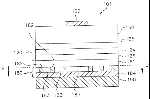
(RS-LED) 101 according to an exemplary embodiment of the present invention.
Exemplary RS-LED 101 provides advantageous light output by reflecting light
emitted
downwardly (away from its top window). RS-LED 101 shown in Figs. 8 and 9 also
advantageously distributes current such that the light-emission profile is
shifted from
below the optically opaque top contact, allowing more of the emitted light to
exit the
device.
[0023] As used in this document, the terms top, over, upwardly, and the like
indicate a direction toward the top of the corresponding figure which also
corresponds
to the direction from which light is emitted from the completed device. The
term
transparent means that light (in the relevant frequency range) passes through
the
composition or structure with little or no absorption.
[0024] Exemplary RS-LED 101 of Fig. 8 comprises, from top to bottom, a top
contact 109, a top window 160, an active region 120, a bottom window 161, a
reflector
180, and a conductive holder 190. Active region 120 comprises an emitting
region 124
sandwiched between a bottom confinement layer 126 and a top confinement layer
125.
The device illustrated in Fig. 8 and described below is preferably grown in a
P-up
configuration: the semiconducting structures gown after the light-emitting
region 124
are P-type and the semiconducting structures grown before the light-emitting
region
124 are N-type. It should be noted, however, that embodiments with an N-up
configuration are also contemplated within the scope of the invention. Even
though a p-
type up growth is generally preferred, n-type-up growth is possible.
[0025] Top confinement layer 125 may comprise, for example, AIGaInP doped
with a P-type dopant such as Mg or Zn ions at a concentration of between about
5.OEE16 and 1.OEE18 atm/cm3. Bottom confinement layer 126 may comprise, for
example, AlGaInP doped with an N-type dopant such as Si or Te ions at a
concentration
of between about 5.OEE16 and 1.OEE18 atm/cm3. Emitting region 124 may
comprise,
for example, a semiconducting layer of uniform composition, a double
heterostructure
(DH), or, more commonly, a multiple quantum well (MQW) structure comprising
AIGaInP.
CA 02470095 2004-06-11
WO 03/052838 PCT/US02/39846
[0026] Top and bottom windows 160, 161 each comprise a transparent,
electrically conductive material, such as GaP, AIGaInP, AlInP, AIGaAs or GaInP
with a
low In content. Top window 160 may comprise, for example, AlGaInP doped with a
P-
type dopant such as Mg or Zn ions at a concentration of between about 1.0EE17
and
5 1.OEE19 atm/cm3. Bottom window 161 may also comprise AIGaInP doped with an N-
type dopant such as Si or Te ions at a concentration of between about 1.0EE17
and
1.OEE19 atm/cm3. Windows 160, 161 are generally transparent, absorbing only a
minor fraction of the light transmitted through them. It should be noted that
GaP
should only be used for the top or bottom window 160, 161 grown after active
region
120, because the GaP lattice would cause a mismatch with an AIGaInP lattice
that is
lattice-matched to the GaAs substrate. Top window 160 has a thickness of
between
about 1 and 25 microns, preferably between about 5 and 20 microns. Bottom
window
161 has a thickness of between about 1 and 25 microns, preferably between
about 1
and 15 microns. Top window 160 spreads current beyond the boundary of top
contact
109, as shown in Fig. 10. Bottom window 161 spreads current between ohmic
contacts
182.
[0027] Reflector 180 comprises a transparent layer 183, an array of ohmic
contacts 182, and a reflective film 184. Transparent layer 183 has a low index
of
refraction, preferably between about 1.10 and 2.25. In the exemplary
embodiment
illustrated in Figs. 8 and 9, transparent layer 1,83 comprises a low
refractive index
insulating material, such as silicon dioxide (SiO2), silicon nitride (Si3N4).
or Magnesium
fluoride (MgF). The thickness (th) of transparent layer 183 is approximated by
the
equation:
th = A/(4n) (eq. 1)
where A is the peak emission wavelength of the LED and n is the refractive
index of
transparent layer 183. This thickness helps to ensure that light, which
strikes
transparent layer 183 over a wide range of incident angles, is reflected with
high
reflectivity.
[0028] Extending through transparent layer 183 is an array of ohmic contacts
182 configured in a pattern 181. Ohmic contacts 182 define a central portion
185, in
transparent layer 183, positioned to correspond to top contact 109. Ohmic
contacts
182 provide a low resistance electrical contact with the overlying
semiconductor layers
and may comprise, for example, a metal composition, such as AuGe-Ni-Au for N-
type
ohmic contacts and AuZn or AuBe for P-type contacts. As shown in Fig. 9, ohmic
contacts 182 comprise a small fraction of the interface area between
reflective film 184
and bottom window 161. Ohmic contacts 182 comprise between about 0.25 and 10
CA 02470095 2004-06-11
WO 03/052838 PCT/US02/39846
6
percent of the interface area. This small ohmic contact surface area increases
the
portion of light that reaches and is reflected by the underlying reflective
film 184.
Increased reflection, in turn, increases the light extraction efficiency of
the LED.
[0029] Pattern 181 enhances the current-spreading function of top window 160.
As shown in Fig. 10, electrical current is prevented from passing through
insulating
transparent layer 183, including central portion 185 of insulating transparent
layer 183,
and is instead drawn toward contacts 182. Note that contacts 182 do not
underlie top
conductor 109. Thus, the current distribution (represented by the width of the
dashed
light-emission profile 124A) in emitting region 124 is greater in the portions
of emitting
region 124 beyond top conductor 109 than in the portion of emitting region 124
underlying top conductor 109. Consequently, a smaller portion of the emitted
light is
reflected, scattered, or absorbed by opaque top contact 109.
[0030] Reflective film 184 comprises an electrically conductive material that
has
a high reflectivity, serving as both an electrical contact and a reflector.
Suitable
materials for reflective film 184 include silver (Ag) and aluminum (Al). The
thickness
and low refractive index of transparent layer 183 coupled with the high
reflectivity of
reflective film 184 cause nearly all of the light emitted downwardly to be
reflected
rather than absorbed, enhancing extraction efficiency.
[0031] Conductive holder 190 shown in Fig. 8 is attached to reflective film
184,
providing structural stability and electrical contact. Conductive holder 190
may be, for
example, a conductive metal structure or a silicon wafer with a metal coating
on its top
and bottom faces. Active region 120 and windows 160, 161 of RS-LED 101 are
thin,
less than 50 microns thick and, as a result, are mechanically fragile.
Conductive holder
190 has a sufficient thickness to provide structural stability. In an
exemplary
embodiment, the interface of reflective film 184 and conductive holder 190 is
metal-to-
metal. Therefore, conductive holder 190 can be mechanically and electrically
connected to reflective film 184 using a high-yield process, such as soldering
or gluing
using a conductive adhesive, thus avoiding the semiconductor-to-semiconductor
wafer-
bonding problems of TS-LED 11.
[0032] Referring to Figs. 11-17, an exemplary method is provided for forming a
RS-LED 101. Bottom window 161, active region 120, and top window 160
(collectively
comprising semiconducting or epitaxial layers) are sequentially formed on a
GaAs
substrate 201. The epitaxial layers may be formed, for example, using a Metal-
Organic
Vapor Phase Epitaxial (MOVPE) process with an AlGaInP chemistry. Bottom window
161 is preferably deposited or grown to a thickness of about 1 to 15 micron.
Bottom
confinement layer 126 is deposited or grown over bottom window 161. Bottom
CA 02470095 2004-06-11
WO 03/052838 PCT/US02/39846
7
confinement layer 126 may be deposited or grown, for example, by continued
MOVPE.
Window layers and confinement layers are doped to ensure electrical
conductivity of
the layers and the formation of a PN junction.
[0033] An AlGaInP light-emitting region 124 is formed over bottom confinement
layer 126. Emitting region 124 may comprise, for example, a DH or MQW
structure as
are known in the art. Next a top confinement layer 125 and a top window 160
are
sequentially deposited or grown over emitting region 124. Both top confinement
layer
125 and top window 160 are doped with a P-type dopant such as Mg or Zn ions,
with
top window 160 having a greater dopant concentration than top confinement
layer 125.
Alternatively, an AlInP, or AIGaAs chemistry may be used in place of the
AlGaInP
chemistry for windows 160, 161. Also, a GaP chemistry may be used for top
window
160 formed after active region 120 in the present method.
[0034] After the epitaxial layers are deposited or grown using a MOVPE
process,
top contact 109 is formed over top window 160. Top contact 109 may comprise,
for
example, a conductive metal such as a AuZn or AuBe alloy covered by aluminum
or
gold formed by a deposition and patterning process. Such alloys form a contact
to P-
type semiconductors. Then, a temporary holder 203 is attached to top contact
109 and
top window 160 by wax or other removable substance, and substrate 201 is
removed
from the epitaxial layers. The bulk of substrate 201 may be removed by a
chemical-
mechanical polishing process, with about the final 20 microns being removed by
selective wet chemical etch.
[0035] Back-side processing, shown in Fig. 15, is performed after removal of
substrate 201. Pattern 181 of ohmic contacts 182 is formed, extending through
transparent layer 183 with a low index of refraction. Transparent layer 183
may be
formed by deposition on bottom window 161 with the epitaxial layers inverted
(i.e.,
with temporary holder 203 down, opposite from the position shown in Fig. 15),
then
patterned to form openings for ohmic contacts 182 using a photolithography
process.
Ohmic contacts 182 may then be formed by another photolithographic process. As
described above, ohmic contacts 182 may comprise a metalization such as AuGe-
Ni-Au.
Such alloys form a contact to N-type semiconductors.
[0036] Alternatively, pattern 181 may be formed by blanket deposition of a
metal layer and patterning the blanket metal layer. Transparent layer 183 may
then
be formed over pattern 181 and planarized to expose ohmic contacts 182.
Alternatively, transparent layer 183 may be blanket deposited and patterned to
form
contact vias. Reflective film 184 is then formed over transparent layer 183
and ohmic
CA 02470095 2004-06-11
WO 03/052838 PCT/US02/39846
8
contacts 182, providing electrical continuity between reflective film 184 and
the
epitaxial layers through ohmic contacts 182.
[0037] Conductive holder 190 is attached to reflective film 184 by conductive
adhesive, soldering, or another process providing mechanical attachment and
electrical
connection. It should be noted that attachment of conductive holder 190 to
reflective
film 184 does not require the precision wafer-to-wafer bonding associated with
TS-LED
11. After conductive holder 190 is attached, temporary holder 203 is removed.
[0038] An alternative exemplary RS-LED 301 is shown in Figs. 18 and 19.
Epitaxial layers 160, 120, 161 and top contact 109 are similar to the
exemplary
embodiment described above and illustrated in Figs. 8-17. Alternative RS-LED
301
comprises a reflector 380 subjacent bottom window 161. Reflector 380 comprises
a
refractive layer having a conductive low refractive index region 382 and an
insulting
low refractive index region 383. Conductive low refractive index region 382 is
configured with a central portion 385 positioned to correspond to top
conductor 109.
Conductive low refractive index region 382 may comprise an electrically
conductive
material such as InSnO, frequently referred to as ITO, having an index of
refraction
between about 1.10 and 2.25. Insulating low refractive index region 383 may
comprise
an electrically insulating material, such as Si02 or Si3N4, having an index of
refraction
between about 1.10 and 2.25. Insulating low refractive index region 383 is
formed at
least in central portion 385. As with the embodiment described above, the
thickness
(th) of the refractive layer is approximated by Equation 1 (th = A/4n).
[0039] An alternative exemplary method for forming the RS-LED is illustrated
in
Figs. 20-24. Epitaxial layers 160, 120, 161 are grown or deposited on a GaAs
substrate 201 as described above. Following formation of the epitaxial layers,
back-
side processing is performed as shown in Fig. 21. Insulating low refractive
index layer
183 is formed and patterned, followed by deposition of ohmic contacts 182 in
insulating
low refractive index layer 183. Alternatively, an ohmic contact layer may be
blanket
deposited and patterned to form ohmic contacts 182, with insulating low
refractive
index layer 183 deposited between ohmic contacts 182. Planarization steps may
be
performed as required. Reflective metallic film 184 is then formed over ohmic
contacts
182 and insulating low refractive index layer 183. The materials and thickness
of
ohmic contacts 182, insulating low refractive index layer 183, and reflective
film 184
are similar to the embodiment described above.
[0040] Conductive holder 190 is attached to reflective film 184, as shown in
Fig.
. 22. Then, substrate 201 is removed, as shown in Fig. 23, and top contact 109
is
formed over top window 160 as shown in Fig. 24. This alternative exemplary
method
CA 02470095 2004-06-11
WO 03/052838 PCT/US02/39846
9
allows bottom window 161 to be formed after active region 120, so that bottom
window
161 may be GaP or other materials that are lattice-mismatched with respect to
GaAs.
[0041] It is generally known that surface texturing (also called surface
roughening) of an LED can increase the light extraction efficiency of an LED.
Surface
texturing of the top surface of the LED has proven to be particularly
effective. Surface
texturing may include random roughening, the fabrication of grating
structures, and
the fabrication of photonic bandgap structures. Surface-textured structures
would be
well known to a person skilled in the art. Such surface texturing may also be
applied in
the present invention to increase light-extraction from the LED. For example,
the top
surface of layer 160 in Fig. 8, Fig. 10, or Fig. 18 may be surface textured.
[0042] Although illustrated and described above with reference to certain
specific embodiments, the present invention is nevertheless not intended to be
limited
to the details shown. Rather, various modifications may be made in the details
within
the scope and range of equivalents of the claims and without departing from
the spirit
of the invention.