Note: Descriptions are shown in the official language in which they were submitted.
CA 02470698 2004-06-16
WO 03/052454 PCT/GB02/05796
MOTION DETECTOR
Field of the Invention
The present invention relates to a detector and,
more particularly, to such a detector comprising a self-
diagnosis capability.
Background to the Invention
Present day motion detectors rely upon the Doppler
principle, as is well known within the art, to detect the
presence of a moving object within a protected volume or
volume to be surveyed. Conventionally, such motion
detectors use at least microwave technology, that is,
typically X-band or K-Band signals transmitted and
received via a transceiver. Post-reception, the received
signals are suitably processed to identify the presence
of a Doppler signal that can be attributed to movement
within the protected volume.
Relatively sensitive devices such as, for example,
the mixer, which typically takes the form of a mixer
diode, can be easily damaged by inappropriate handling or
excessive signal strengths. Therefore, care needs to be
taken in the fabrication and the installation of the
motion detectors. Notwithstanding any such care, the
mixer diodes may, post-installation, be inappropriately,
exposed to signals or handling that may cause damage. It
will be appreciated that any such damage may, in the
worst case, prevent the motion detector from operating
correctly in that, from the perspective of the output of
the mixer diode, there will be no change in the signal
due to any Doppler shifted received signal.
Alternatively, the performance of the mixer diode may be
degraded in some way so that it produces excessive noise,
which reduces the sensitivity of the motion detector.
Printed: 22-03-2004 DESCPAMD C GB0205796
2
It is an object of the present invention at least to
mitigate some of the problems of the prior art.
Summary of Invention
Accordingly, a first aspect of embodiments of the
present** invention provides a detector comprising a mixer
for combining at. least first and second electro-magnetic
signals to produce a combined signal having a
predetermined characteristic.; a conductor for coupling at
least the first electro-magnetic signal to the mixer; and
a device, disposed relative to the conductor, to impose,
in response to an input signal, 'a variable load on the
conductor to thereby vary at least one of the phase and
magnitude of the first electro-magnetic signal; the
variation being manifested in a further* predetermined
characteristic of the combined signal.
Preferably, embodiments provide a detector a
detector in which the device is physically unconnected
with the conductor. Alternative embodiments are provided
in which the device is physically connected with the
conductor.
Preferably, an embodiment is provided in which the
device comprises a semi-conductor device disposed
adjacent to the conductor carrying the first' signal. It
will be appreciated that the semi-conductor device should
be positioned sufficiently close to the conductor so as
to be able to influence the electro-magnetic field of the
signal being carried by-the conductor.
In a preferred embodiment, the degree of influence
exerted by the device varies-with variations in the input
signal. Preferably, the input signal is modulated. at a
predetermined frequency. The predetermined frequency is
preferably between 10Hz and 8OHz,-.which frequencies are
3 CA 02470698 2004-06-16 AMENDED SHEET 23- ! 2 2003
Printed: 22-03-2004 DESCPAMD CGB0205796
3
typical Doppler frequencies that would be generated by a
human moving within a protected volume. Furthermore,
these are frequencies that the IF amplifiers in such a
detector would pass. Additionally,, the input signal is
arranged to switch the device between substantially open
and substantially closed circuit conditions.
Furthermore, the device is operable in response to the
input signal to present substantially closed or open
circuit conditions to the first electro-magnetic signal
carried by the conductor.
In preferred embodiments, the device does not
radiate or generate an electro-magnetic field in response
to the input signal. The device merely represents a
variable load on the conductor.
In a preferred embodiment the semi-conductor device
is a diode.
It will be appreciated that-the output of the mixer,
having had one of the input signals influenced by the
device, can be used by a signal analysis system
comprising, for. example, a micro-processor and associated
software, to determine whether or not the mixer and/or
the device as a whole is functioning correctly.
Suitably, an embodiment additionally comprises a signal
analyser for analysing the combined signal to determine
whether that combined signal has the further
predetermined characteristic. In preferred embodiments,
the predetermined characteristic includes at least an
oscillation having a frequency that is associated with
the frequency of the input signal.
To test- the operation of the mixer an appropriate
input _signal should be applied to the device. Suitably,
an embodiment provides a signal generator for generating
the input signal to be applied to the device for
2` CA 02470698 2004-06-16 AMENDED SHEET 23-12-2003
Printed. 22-03-2004 DESCPAMD CGB0205796
jl
4
influencing the electro-magnetic fiel.a..
It will be appreciated that t,e second signal fed
into the mixer is conventionally a d.,i prided portion of the
output of a local oscillator; the ether portion having
been, in operation, radiated by a t1_ansmit antenna. In
the absence of motion, the RF signal on the input to the
mixer is at the same frequency as, the LO signal. The
mixer then operates as a phase detector and produces a DC
voltage at its output that is rLated to the phase
difference between the LO and I,, signals and the
magnitude of the RF signal. Hence, by disturbing at
least the phase and, preferably, th phase and magnitude
of the RF input signal to the mix r, an output signal
indicative of that disturbance will( be produced by the
mixer.
Embodiments of the present invention are preferably
provided in which the first electrod=e-magnetic signal is
derived from the transmitted signal. j
Further embodiments are provided in which the second
signal is derived from the received dgnal.
Still further embodiments provide a detector further
comprising signal analyser fof monitoring the
predetermined characteristic of the combined signal to
determine the correct operation or otherwise of at least
one element of the detector.
Preferably, the at least one element is at least one
of a mixer, transmitter,.oscillator ahnd received portion.
is are w .'
Embodiments provided ~n Y:..ch the device does
not radiate an electro-magnetic fiel~p in response to the
input signal.
3 CA 02470698 2004-06-16 AMENDED SHEET 11 [23-12-2003,
Printed: 22-03-2004 DESCPAMD CGB0205796
4a
Other embodiments are provided in which the device
is arranged to radiate an electro-magnetic field in
response to the input signal.
Embodiments provide a detector in which the
conductor is a local oscillator conductor leading to a
local oscillator RF port of the mixer and the first
electrode-magnetic signal is a local oscillator signal.
Embodiments provide a method of operating a detector
comprising a mixer for combining at least first and
second electro-magnetic signals to produce a combine
signal having a predetermined characteristic; a first
conductor for coupling at the least the first electro-
magnetic signal to the mixer; and a device, disposed
relative to the conductor, to impose, in response to an
input signal, a variable-load on the conductor to thereby
vary at least one of the phase magnitude of the first
electro-magnetic signal; the variation being manifested
in a further predetermined characteristic of the combined
signal; the method comprising the step of generating
first and second electro-magnetic signals; applying the
input signal to the device to vary the load imposed by
the device on the conductor; and deriving a measure of
the correct operation or otherwise from the combined
signal.
Embodiments provide a method further comprising the
step of operating the device, in response to the input
signal, to produce a predetermined circuit condition
experienced by at least one of t=he first and second
electro-magnetic signals:
4 AMENDED SHEET 23-12-2003
CA 02470698 2004-06-16
Printed: 22-03-2004' DESCPAMD C GB0205796
4b
Embodiments provide a= method in which the
predetermined circuit condition is an open circuit
condition.
Embodiments provide a method in which the
predetermined circuit condition is a closed circuit
condition-
Brief Description of the Drawings
Embodiments of the present invention will now be
described, by way of example only, with reference to the
accompanying drawings in which:
figure 1 illustrates schematically a motion
detection system having a self-diagnosis capability in
accordance with a first embodiment of the present
invention;
figure 2 illustrates a detector for use in such a
motion detection system in accordance with an embodiment;
and
figure 3 illustrates a detector for use in such a
motion detection system in accordance with a further
embodiment.
Description of the Preferred Embodiments
5 CA 02470698 2004-06-16 AMENDED SHEET 23-12-2003
CA 02470698 2004-06-16
WO 03/052454 PCT/GB02/05796
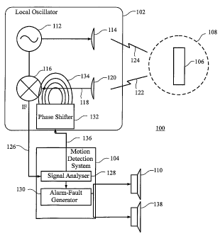
Referring to figure 1 there.is shown schematically a
motion detection system 100 comprising a detector 102
which co-operates with a detection system 104 to detect
relative motion between the device and a body 106 within
5 a monitored volume 108 and to produce a corresponding
alarm signal via an output device 110 in response to the
detection of any such relative motion. The output device
may be an -audio-visual output device.
The detector 102 comprises a local oscillator 112
for generating K or X-band microwave signals that are
radiated into the monitored or protected volume 108 via a
transmit antenna 114. A portion of the output of the
local oscillator signal 112 is directed towards a mixer
116 which combines that portion with an RF input signal
122, carried on a conductor 118, that has been received
by a receive antenna 120. Typically, in the presence of
relative motion between the device and the body, the RF
input signal 122 is a reflected and Doppler shifted
version of the transmitted signal 124. The output of the
mixer, that is, the IF signal 126, is input into the
detection system 104 which, if appropriate, can instruct
an alarm-fault generator 130 to generate an appropriate
alarm signal to be output via the audio-visual output
device 110.
The detector also comprises a device 132 for
influencing the electro-magnetic field of the RF input
signal being carried by the conductor 118. The device
132 is operable to present a variable load to the nearby
microstrip 118 in response to an applied signal 136. As
the signal 136 is applied to the device, its loading
effect upon the nearby microstrip 118 changes, which, in
turn, changes the electrical 'characteristics of the line
118 from the perspective 'of the RF signal. Preferably,
the device 132 takes the form of a diode that, in
CA 02470698 2004-06-16
WO 03/052454 PCT/GB02/05796
6
response to the applied signal 136, causes a change in
the electro-magnetic field carried by the conductor 118.
In particular, the device influences the phase of the RF
input signal (at the RF input port) of the mixer 116.
In the absence of motion, the mixer 116 acts as a
phase detector and produces a DC output signal in
response to receiving an input signal on the port that
would ordinarily receive the received signal 122,. that
is, on the RF input port of the mixer. This input signal
is a combination of the received signal 122 reflected
from static objects within the protected volume 108 and
signals generated within the detector 102 due to internal
reflections.
Referring to figure 2 there is shown in greater
detail a circuit 200 for realising an embodiment of the
detector 102. The circuit 200 comprises a local
oscillator circuit 202, that is coupled, via a decoupling
capacitor 204, to a transmit antenna feed portion 206 and
a receive antenna portion 208 of the circuit. The device
also comprises a test portion 210. The various portions
202 to 210 are' screened via appropriate planar
metalisations 212 having holes drilled therein to
suppress unwanted spurious electro-magnetic emissions
from the various circuit elements.
A series of connection tabs 214 are provided to
allow power to be supplied to the circuit elements 202 to
210 and to allow the IF. signal to be received as well as
to allow a test signal, that is, input signal, to be
applied to the test portion 210. The connection tabs 214
30' comprise a ground connection tab 216 and an IF output
connection tab 218. The IF output connection tab 218
also serves as the output for the signal generated as a
result of testing the operation of the receive portion
CA 02470698 2004-06-16
WO 03/052454 PCT/GB02/05796
7
208. It will' be appreciated that the test diode 242
tests the whole of the operation of the detector, that
is, the local oscillator, the mixer and the transmit and
receive antennas. A test signal connection tab 220 is
arranged to provide the test signal to the test portion
210 of the device. Power is supplied to the local
oscillator circuit 202 via a power connection tab 222.
The local oscillator circuit 202 comprises, in a
preferred embodiment, a dielectric puck 224 disposed
adjacent to a pair of strip lines 226 and 228 that are
connected to one another via the,gate and drain of a FET
transistor. Power is supplied to the transistor via the
power connection tab 222 and a resistor 230. The output
of the transistor is coupled via the decoupling capacitor
204 to the transmit and receive portions 206 and 208
where that power is divided in a predetermined ratio.
The power carried by a microstrip line 232 of the
transmit portion 206 is coupled via a slot in a ground
plane (not shown), preferably, to a pair, of patch
transmit antennas (not shown) as is well known within the
art. An example of a detector within which embodiments
of the. present invention can be incorporated is shown in
UK patent application no. GB2253108, the content of which
is incorporated herein for all purposes.
Similarly, power is coupled to a microstrip line 234
of the receive portion via a corresponding slot in a
ground plane (not shown) and an associated pair of patch
receive antennas (not shown).
It can be appreciated that the diode mixer 236 of
the receive portion 208 receives power from the local
oscillator via a corresponding microstrip line 238 and
also from the microstrip line, 234. The output of the
mixer diode 236 is fed to the IF output tab 218 for
CA 02470698 2004-06-16
WO 03/052454 PCT/GB02/05796
8
further processing by the detection, system 104 and, more
particularly, by a signal analyser 128.
The test portion 210, in a preferred embodiment,
comprises the series arrangement of a resistor 240 and
the test diode 242. The diode 242 is disposed within
close proximity to a conductor or microstrip line 244
which couples power from the receive microstrip line 234
to the receive RF input of the diode mixer 236. . The
diode 242 is positioned sufficiently close to the
microstrip line conductor 244 such that, in the presence
of the input signal applied to the test signal connection
tab 220, the variation in diode 242 characteristics is
sufficient to vary the degree of influence experienced by
the electro-magnetic field of the signal being coupled
from the receive microstrip line 234 to the receive RF
input of the diode mixer 236 in the vicinity of
microstrip line 244. In a preferred embodiment, the
electro-magnetic field perturbation caused by the change
in diode characteristics in response to the applied
signal imparts at least a phase change to the signal
carried by the microstrip line 244. As the microstrip
line 244 couples power to the RF port of the mixer, that
is, the receive RF input of the diode mixer 236, a
corresponding phase change occurs at the RF port of the
mixer.
It will be appreciated in the absence of motion,
that is, in the absence of the received signal being a
Doppler shifted version of the transmitted signal, that
the mixer diode 236 operates as a phase detector which
generates a DC voltage that is dependent upon the
relative phases and magnitudes of the signals present at
the local oscillator input port and the RF input port of
the mixer. The two signals,are-in fact each the resultant
of a vector summation of all signals appearing at each of
CA 02470698 2004-06-16
WO 03/052454 PCT/GB02/05796
9
the two ports. Therefore by influencing one of those
signals, as in the preferred embodiment, the phase of the
resultant signal at the RF input port could be changed.
In turn this will change the DC voltage present on the IF
output tab 218.
Preferably, the test signal applied to the test
signal connection tab 220 is arranged to be a TTL signal
(OV to +5V) at a frequency that is within the bandwidth
of the amplifiers contained within the signal analyser
128 that is connected to the IF output tab 218. For
example, embodiments may use a test signal having a
frequency of 30Hz.
The detection system 104 uses the signal analyser
128 to monitor the IF output 218 to determine whether or
not an intrusion into the protected volume 108 has been
detected during conventional operation of the system 100.
In the event that the signal analyser 128 determines that
an intrusion into the protected volume 108 has been
detected, the signal analyser 128 instructs the alarm-
fault signal generator 130 to produce at least one of an
audible or visual alarm signal via the output device 110.
or to output an alarm condition signal for further
processing by, for example, a central control centre.
However, during a test mode of operation of the
detection system, the signal analyser 128 supplies an
appropriate test signal to the test signal connection tab
220 during the normal operation of the detector 102, that
is, during the conventional transmit and receive
operations of the detector 102. The signal analyser 128,
again, monitors the IF output tab 218 and in the absence
of the IF output signal meeting predetermined criteria,
the signal analyser 128 instructs the alarm-fault
generator 130 to produce a fault indication signal that
CA 02470698 2004-06-16
WO 03/052454 PCT/GB02/05796
is output via a fault indicator 138. It will be
appreciated that the testing preferably takes place in
the absence of motion of a body within the protected
volume. The predetermined criteria include the magnitude
5 of the IF signal being disposed above or below a
particular threshold. The fault indication signal can
equally well or additionally be output to a central
control centre.
Preferably, the test signal generated in the
10 embodiments of the present invention does not saturate
any IF amplifiers that may be present. For example, the
input signal may be arranged to produce a 3Vpk_pk signal at
the output of the IF amplifier. It will be appreciated
that the signal output by the mixer will vary according
to whether or not an object enters the protected volume.
Therefore, by applying the test signal and looking for a
deviation from an anticipated peak-to-peak voltage output
signal from the IF amplifiers, a change in the presence
or otherwise of an object within the protected volume may
be detected. ' Therefore, if an object enters a protected
volume and becomes stationary, when the testing is
applied, rather than the monitoring system detecting the
anticipated, or previous equilibrium, voltage level, a
new voltage level will be detected. The change in the
voltage provides an indication that the scene has
changed, that is, that one or more objects have been
removed from or introduced into the protected volume
since the last investigation by the monitoring system
104.
Advantageously, the correct operation or otherwise
of the detector 102 can be monitored in a predetermined
and controlled manner and also in the absence of external
test equipment that is conventionally used to monitor
such operation.
CA 02470698 2004-06-16
WO 03/052454 PCT/GB02/05796
11
Figure 3 illustrates a detector 300 for use in such
a motion detection system in accordance with a further
embodiment. The detector 300 of figure 3 is
substantially similar to that of figure 2, with like
reference numerals being associated with like elements,
which perform substantially the same functions. Figure 3
illustrates a number of possible positions for the
loading device, that is, the diode, in preferred
embodiments. It can be appreciated that the diode can be
positioned at one of five locations D1-1 to D1-5
associated with the RF receive path and two additional
locations D1-6 and D1-7 associated with the local
oscillator signal path. One skilled in the art will
realise that these diodes may be selectively used or
selectively provided as part of the circuit as they see
fit. Therefore, in some embodiments, the monitoring
system has the option of using one or more diodes in a
testing procedure both jointly and severally. The two
diodes positions D1-2 and D1-3 adjacent to the RF
microstrip 244 are used to provide increased loading on
that microstrip 244. The diode positions D1-4 and D1-5
adjacent to the slot 234 are arranged to have a
significant influence on the RF signal passing through
the slot. The final RF diode position D1-1 is adjacent
to the "U" of the mixer.
Two diode positions are provided adjacent to the LO
input. These positions are D1-6 and D1-7. Preferably,
these diode positions are orthogonal to each other.
The diodes in the various positions may be used
jointly or severally in testing the detector or
investigating the protected volume.
It will be appreciated that a conventional diode,
such as a BAS 16, can be used in the preferred
CA 02470698 2004-06-16
WO 03/052454 PCT/GB02/05796
12
embodiments. However, the embodiments are not restricted
to such an arrangement. Embodiments can equally well be
realised in which other devices could be used such as,
for example, a microwave diode, a FET, a further mixer or
the like, providing the characteristics of the device
vary in response to an applied test signal in such a
manner as to influence the electro-magnetic field carried
by the microstrip lines to the RF input of the mixer.
Although the above embodiments have been described
with reference to detecting movement within a protected
volume, the present invention is not limited to such an
application. It will be appreciated by those skilled in
the art that the invention is equally applicable to
relative motion between the detector and a body whether
the body is stationary and the detector is moving or both
the body and detector are moving relative to each other.
The above embodiments have been described with
reference to a device that influences or modifies the
electro-magnetic field carried by the conductor. It does
not radiate electro-magnetic energy as a microwave
oscillator would for example, at least not intentionally
or not to a sufficient degree to influence the field
carried by the conductor. However, it will be
appreciated that embodiments of the present invention can
be realised in which the device does radiate an electro-
magnetic field, in response to an input signal or
otherwise, which influences the signal or electro-
magnetic field present at the RF input port of the mixer.
The field present at that port will be generated by
superposition of the generated field and the received RF
field. This superposition may be in addition to the
influencing of the field described above in the preferred
embodiments.
CA 02470698 2012-01-31
WO 03/052454 PCT/GB02/05796
13
Although the above embodiments have been described
with reference to influencing the RF signal, embodiments
are not limited to such arrangements. Embodiments can
equally well be realised in which the device is disposed
sufficiently close to one of the other microstrip lines.
leading to the mixer to influence electro-magnetic
signals carried by those lines. Again, any such
influence will manifest itself in a change in the output
signal of the IF port of the mixer., For example; the
device may be disposed so as to influence the signals
carried by the local oscillator microstrip line that
leads to the local oscillator port of the mixer. By
influencing the characteristics of this line, the return
loss or reflection coefficients for this line may be
influenced. This, in turn, may lead to corresponding
variations in the conversion loss for the mixer. That
is, if the conversion loss of the mixer varies due to the
influence exerted by the'diode on the conductor, then the
dc output at the IF port, due to the mixer acting as a
phase detector, when there is no movement within the
protected volume, will also vary thereby providing an
indication that the detector is functioning correctly.
The reader's attention is directed to all papers and
documents which are filed concurrently with or previous
to this specification in connection with this application
and which are open .to public inspection with this
specification, and the contents of all such papers and
documents.
All of the features disclosed in this specification
(including any. accompanying claims, abstract and
drawings) and/or all of the steps' of, any method or
process so disclosed, may be combined in any combination,
except combinations where at least some of such features
and/or steps are mutually exclusive.
CA 02470698 2004-06-16
WO 03/052454 PCT/GB02/05796
14
Each feature disclosed in this specification
(including any accompanying claims, abstract and
drawings) may be replaced by alternative features serving
the same, equivalent or similar purpose, unless expressly
stated otherwise. Thus, unless expressly stated
otherwise, each feature disclosed is one example only of
a generic series of equivalent or similar features.
The invention is not restricted to the details of
any foregoing embodiments. The invention extends to any
novel one, or any novel combination, of the features
disclosed in this specification (including any
accompanying claims, abstract and drawings), or to any
novel one, or any novel combination, of the steps of any
method or process so disclosed.