Note: Descriptions are shown in the official language in which they were submitted.
CA 02470792 2004-06-17
WO 03/052369 PCT/US02/38300
SENSOR FORMED ON SILICON ON INSULATOR
STRUCTURE AND HAVING REDUCED POWER UP DRIFT
BACKGROUND OF THE INVENTION
The present invention relates generally to semiconductor-based sensors and
specifically to silicon on insulator (SOI) based sensors.
A diaphragm type silicon based pressure sensor will be used as an example to
describe a problem with sensors in the past. Such pressure sensors typically
include
piezoresistors positioned to sense strain associated with pressure and
arranged in a
Wheatstone bridge to which a direct current voltage is applied. The output
voltage of
the bridge is representative of the pressure that is being sensed. A power up
drift (PUD)
phenomena has been observed in silicon-based sensors that is not explained by
a small
thermal rise that may occur after power is applied to the sensor. A PUD effect
as great
as 0.05% of full scale has been observed.
The PUD phenomena is apparently a result of mobile ions present either on the
surface of the silicon chip or within the silicon dioxide passivation layer,
which have
one preferred configuration with power off and a second preferred
configuration when
power is applied. In other words, these ions are mobile in response to the
application of
voltage to the silicon chip. As the charges move they apparently affect the
characteristics of the circuit elements on the chip. The charges may reside in
any of a
number of locations in the integrated circuit. They may be in the silicon, in
insulating
layers on or under the silicon, at the interfaces between two of these layers,
or at the
surface of the silicon chip. Sensors, including pressure sensors, are often
designed with
a bridge configuration to minimize this and other performance limitations. In
a bridge
configuration, the change of any one element resulting from the redistribution
of
charges on power up is not significant as long as its balancing element
undergoes the
same change. Therefore, great care is usually taken in the design of a sensor
to insure
that the individual elements of the bridge are as identical as possible. The
power-up
drift of the bridge output "resets" itself after the power is removed to the
value that
existed before power was applied. The time required after power is applied for
the PUD
to stabilize is typically less than the time required for the sensor to
"reset" after the
power is removed.
CA 02470792 2004-06-17
WO 03/052369 PCT/US02/38300
Silicon-on-insulator (SOI) based sensors offer several performance advantages
over conventional bulk-silicon based sensors due to the elimination of the p-n
junction.
In bulk silicon, the p-type piezoresistors are implanted or diffused into an n-
type
epitaxial layer, which results in the formation of a p-n junction. The reverse
current
leakage of a p-n junction increases with temperature (approximately doubles
every
10°C), which ultimately limits the operating temperature to typically
125°C. To
minimize the effect of the reverse current leakage, which typically shunts the
piezoresistor element, on performance, the value of the piezoresistive bridge
elements
are typically limited to 40K ohm maximum to maintain quality performance over
temperature.
In SOI, however, the piezoresistor elements are isolated from the silicon
substrate by an insulation layer thereby eliminating the p-n junction and it's
associated
reverse leakage current. The high temperature operating limit of SOI material
is
therefore significantly increased to a range of 200°C to 400°C
depending on the
metalization system, packaging and materials and other variables.
SOI sensors also allow the piezoresistive bridge impedance to be increased to
as
high as 200K ohm with equivalent performance. The higher impedance reduces the
sensor power requirements proportionally. For example, increasing the bridge
impedance from 40K ohm to 200K ohm reduces the sensor power requirement by a
factor of five. These larger impedance values can be achieved without
significantly
increasing the physical area of the piezoresistor element. This is
accomplished in two
ways. First, the effective thickness of the piezoresistor element can be
formed to be
significantly thinner than that formed in bulk silicon which results in a
higher sheet
resistivity (ohms per square) that is inversely proportional to the thickness.
Secondly,
the impurity concentrations of the diffused or implanted piezoresistor can be
reduced,
without performance degradation, which also results in an increase in sheet
resistivity.
The combination of the two methods can result in a five-fold increase in sheet
resistivity
for the same form of the resistor area.
The combination of high temperature operation and power reduction allows SOI
based sensors to be used in many new applications that are beyond the
capability of
bulk-silicon based sensors. Where the sensor application is such that reduced
measurement accuracy is acceptable or where a period of warm-up time is
permissible,
CA 02470792 2004-06-17
WO 03/052369 PCT/US02/38300
the power-up-drift phenomena may not be a problem. However, numerous
applications
require the sensor to met specifications within a very short time, (for
example, a few
seconds or less,) after power is applied. Thus there is a need for a silicon-
on-insulator
sensor configuration that greatly reduces the causes) of power-up drift.
BRIEF SUMMARY OF THE INVENTION
The present invention solves these and other needs by providing a
solution for reducing the power up drift observed in the output of Wheatstone
bridge
configurations of SOI based sensors. In the preferred embodiment of the
present
invention, a sensor has a layer of silicon formed on a silicon substrate, the
layer of
silicon having an insulation layer dividing the layer into an upper and lower
layer.
Within this upper layer, a plurality of resistors are formed, connected in a
bridge
arrangement. The preferred embodiment also includes a means for supplying a
first
voltage to the bridge arrangement and a means for supplying a second voltage
to the
lower layer of silicon. The level of the second voltage is selected to reduce
the power
up drift.
BRIEF DESCRIPTION OF THE DRAWINGS
Figure 1 shows a schematic drawing of a sensor bridge arrangement as
found in the prior art.
Figure 2 shows a cross sectional view of a sensor according to the teachings
of
the present invention.
Figures 3 and 4 are schematic drawings showing additional details related to
the
use of the sensor of Figure 2.
Figure 5 is a diagrammatic representation showing additional details of an
alternative arrangement related to the use of the sensor of Figure 2.
DETAILED DESCRIPTION OF THE INVENTION
A sensor in accordance with the principles of the present invention is shown
in
the drawings and generally designated as reference numeral 10. The present
invention
will be described relative to its application in a silicon based pressure
sensor, but it is to
be understood that it may be used in other applications, for example, in a
temperature
sensor. Sensor 10 includes a network or bridge 12 as shown in FIG. 1 having
one or
CA 02470792 2004-06-17
WO 03/052369 PCT/US02/38300
more piezoresistive devices on a diaphragm, typically of silicon. In the
preferred
embodiment, four such piezoresistive devices are shown in the form of a
bridge. These
four elements are shown as resistors 14, 16, 18, 20. Preferably resistors 14
and 18 are
positioned radially to the diaphragm and resistors 16 and 20 are positioned
tangential to
the diaphragm. In this way resistors 14 and 18 will increase in resistance
with pressure
while resistors 16 and 20 will decrease in resistance for the case where
pressure is
applied to the active side of the diaphragm. In typical operation a constant
input voltage
is applied to terminal 22 and terminal 24 is at ground. This results in an
output voltage
related to the pressure on the diaphragm appearing between output terminals 26
and 28.
Compensation networks, for example to compensate for temperature changes will
also
typically be used, but are not shown for simplicity.
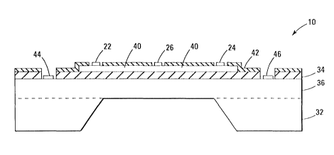
The present invention applies to sensors formed in semiconductor or insulator
structures, for example, a silicon-on-insulator (SOI) structure. SOI
structures may be
formed by various well-known techniques and the present invention may be
practiced
regardless of the method by which the SOI structure was formed. A specific
technique
will be described with reference to FIG. 2. A wafer having an n epitaxial (n-
epi) layer
36 on a p++ substrate is used as a starting wafer. A silicon dioxide layer 34
is formed
beneath the top surface of the n epi layer by high energy oxygen implantion as
in a
SIMOX process. The resulting thin epi layer above oxide layer 34 is used as a
seed
layer to grow an increased thickness of n epi. A thermal oxide layer is then
grown on
the upper n epi layer and consumes a portion of this layer. This thermal oxide
layer is
patterned to allow formation of resistors and boron ions are implanted into
portions of
this remaining thickness of the upper n epi layer to form p+ silicon. A
photomask and
cut process is then used to form individual p+ piezoresistors 40 located as
desired for
the specific bridge and diaphragm configurations. A thermal oxide layer 42 is
then
formed and a contact cut process and metallization is used to form contact 22
at the top,
contact 26 at the center or midpoint, and contact 24 at the bottom of bridge
12. Contact
44 to epi layer 36 near contact 22 or the top of bridge 12 and contact 46 to
epi layer 36
near contact 24 or the bottom of the bridge are also formed. Contacts 44 and
46 are
used according to the principles of the present invention to apply a voltage
to lower epi
layer 36, which is electrically isolated by oxide layer 34 from piezoresistors
40, but
establishes a field that can be used to affect the PUD.
Applying a voltage to the epi layer may provide various configurations:
CA 02470792 2004-06-17
WO 03/052369 PCT/US02/38300
Example l:
The voltage at a midpoint, 60, of the bridge may be connected to the epi
layer as illustrated in FIG. 3.
5 Example 2:
Apply a constant voltage (Vepi) to the n-epi layer that is of a value
between the bridge excitation voltage and ground and that is equal to the
bridge
voltage (Vbridge) times the quantity of one minus the ratio of the magnitude
of the
drift with the n-epi at the bridge excitation voltage (PUD @ Vbridge ) divided
by
the sum of the magnitudes of the drift with the n-epi at the bridge excitation
voltage (PUD @ Vbridge ) and at power ground (PUD @ ground).
In Equation form:
P UD @ Ybridge
1 S YePi - Vbridge 1 ( 1 )
PUD @ hbridge + PUD @ ground
For example: If Vb,.;dge 5 volts; ~(PUD@Vbridge)I =3 units; and ((PUD@ground)~
= 2 units
Then: Vep;=5(1-3/5)=2 volts
This voltage can be provided in a variety of ways.
For example, by providing a resistor divider network as shown in FIG. 4
consisting of resistors R1 and R2 connected in series where the open end of R1
is connected to bridge voltage SO and the open end of R2 is connected to
ground.
Midpoint 52 of the resistor divider network is then connected to the n-epi
layer.
In determining the resistor values, first select the value for the sum of
R1+R2
(1 OK OHMS for example). Then the value of R2 is determined by:
PUD @ Ybridge
R2=(R1+R2) 1- (2)
PUD@Ybridge) + PUD@ground)
CA 02470792 2004-06-17
WO 03/052369 PCT/US02/38300
6
For example: If (R1+R2) is set to l OK OHMS; SPUD @ Vbridgel = 3 units; and
SPUD @
grounds = 2 units
Then: R2= 10(1-3/5)=4 K OHMS and Rl= lOK-R2 - 6K OHMS
The value of R1+R2 can be even larger since the impedance looking into
the n-epi layer is at least in the range of 10~ ohms. Alternatively a voltage
source set to the value as determined by equation (1) can be applied directly
to
the n-epi layer.
Example 3:
Operate the n-epi layer as shown in FIG. 5 with a low frequency pulse
width modulated voltage signal 56 from a source 54 where the high state is
equal
to the Vbridge voltage, for example, 5 volts direct current, and the low state
is
equal to ground. Source 54 provides a square wave voltage 56 and has an
adjustable pulse width. The ratio of the pulse width with respect to the total
period, or the duty cycle, is determined similar to Example 1 above.
For example: If SPUD @ Vb,;dge~ = 3 units; and SPUD @ grounds = 2 units, then
the Pulse Width Ratio = (1-3/5)=.40
A PW Ratio of .40 means that over the period of one cycle, the n-epi
layer will have Vbridge applied for 40% of the time and a ground potential for
60% of the time. Implementation of this concept can be achieved by using
conventional circuit mechanization to achieve the desired low frequency
digital
type signal with pulse width adjustment capability.
Testing also shows that the polarity of the power-up drift is dependent on the
voltage potential applied to n-epi layer 36 indicating that the power-up drift
mechanism
is ionic in nature. The polarity of the drift with the n-epi layer equal to
the bridge
excitation voltage is opposite in polarity to the drift with the n-epi
connected to power
ground.
For bulk silicon based pressure sensors, P-type resistors are implanted
directly
into an N-type epitaxial (n-epi) layer resulting in a p-n junction. Normally,
the n-epi
layer is electrical tie to the bridge excitation voltage via a contact cut
made to the n-epi
layer. This provides a reverse bias to the p-n junction. The n-epi layer
cannot be tied to
a voltage less than the bridge excitation voltage for this would forward bias
the p-n
junction and the sensor would not function correctly.
CA 02470792 2004-06-17
WO 03/052369 PCT/US02/38300
Thus since the invention disclosed herein may be embodied in other specific
forms without departing from the spirit or general characteristics thereof,
some of which
forms have been indicated, the embodiments described herein are to be
considered in all
respects illustrative and not restrictive. The scope of the invention is to be
indicated by
the appended claims, rather than by the foregoing description, and all changes
which
come within the meaning and range of equivalency of the claims are intended to
be
embraced therein.