Note: Descriptions are shown in the official language in which they were submitted.
CA 02470946 2004-06-17
WO 03/052182 PCT/US02/41030
CONTROLLED GROWTH OF SINGLE-WALL CARBON NANOTUBES
Background of the Invention
Carbon nanotubes are seamless tubes of graphite sheets and can be either multi-
walled (MWNT) or single-walled (SWNT). Generally, carbon SWNT are preferred
over carbon MWNT's because SWNT have fewer defects and are stronger and are
better electrical conductors than MWNT's of similar diameter. The structure of
the
SWNT is defined by how the graphite sheet is aligned in a rolled up
configuration.
Carbon nanotubes exhibit technologically important electronic properties and
have
shown promising applications, including nanoscale electronic devices, high
strength
materials, electron field emission devices, tips for scamling probe
microscopy, and
chemical sensors. Most electronic applications of carbon nanotubes require
significant amounts of aligned SWNT that are reasonably homogeneous in
diameter,
length and helicity, since the electronic properties correlate both with the
diameter
and chirality (twist). Carbon nanotubes can be found in both metallic and
semiconducting structures. Metallic nanotubes can carry large current
densities while
semiconducting nanotubes can be electrically switched on and off like field-
effect
transistors (FET's).
Single-walled carbon nanotubes are typically prepared in the presence of a
particulate transition metal catalyst, such as V or Co. However, SWNT prepared
using the particulate catalysts show a rather broad distribution of SWNT
diameters,
with the width of the distribution increasing with the SWNT diameter.
Catalysts, in
CA 02470946 2004-06-17
WO 03/052182 PCT/US02/41030
particular metal catalysts, tend to restructure and sinter under the harsh
reaction
conditions required for SWNT synthesis, leading to the formation of mufti-
faceted
crystals, with each facet potentially initiating the growth of a SWNT and
contributing
to the heterogeneity in diameter and structure.
As a result, no economically scalable methods exist for reliably preparing,
separating or aligning nanotubes of controlled diameter and electronic
properties
either by selective synthesis or through post-synthesis separation. The
inability to
male controlled junctions on the nanoscale is also a limiting factor in making
particular electronic devices requiring local gate layout. Device development
therefore is limited by the lack of control in synthesizing clean aligned
nanotubes of
a specified type. The inability to make controlled junctions on a manometer
scale is
also a limiting factor in malting particular electronic devices requiring
local gate
layout.
It would therefore be desirable to develop a material system and a process for
the
growth of carbon SWNT with better defined chemical and physical propeuties. It
would also be desirable to produce nanoscale devices that incorporate such
SWNT
for electronic and sensing applications.
SummarX of the W vention
The invention, in one aspect, is directed to the growth of carbon SWNT with
controllable physical properties, such as a predetermined diameter and a nan-
ow
diameter distribution, in a catalytic template or catalytic framework. The
prepared
2
CA 02470946 2004-06-17
WO 03/052182 PCT/US02/41030
SWNT can have well-defined electric and/or magnetic characteristics and/or a
selective response to the presence of foreign molecules.
According to one aspect of the invention, a method for producing single-wall
carbon nanotubes includes providing a framework made of an mesoporous
siliceous
structure having a predetermined uniform pore size and containing a metal ions
located only in substitutional sites of the framework, with the dispersed
metal ions
forming the only source of catalytic sites, and flowing a carbon-containing
reactant
over the framework at a predetermined temperature. The method produces single-
wall carbon nanotubes with a diameter that correlates with the predetermined
pore
size.
According to another aspect of the invention, an ordered arrangement of
nanotubes with a nanow diameter distribution includes a framework made of an
mesoporous siliceous structure having a predetermined uniform pore size and
containing metal ions selectively dispersed in substitutional sites of the
framework,
wherein the dispersed metal ions form the only source of the catalytic sites.
The
single-wall carbon nanotubes disposed in the pores of the framework have a
diameter
that correlates with the predetermined pore size.
According to yet another aspect of the invention, a chemical sensor includes
single-wall carbon nanotubes with a narrow diameter distribution. The sensor
is
composed of a framework made of an mesoporous siliceous structure having a
predetermined uniform pore size and containing metal ions selectively
dispersed in
substitutional sites of the framework, wherein the dispersed metal ions form
the only
CA 02470946 2004-06-17
WO 03/052182 PCT/US02/41030
source of the catalytic sites. The single-wall carbon nanotubes disposed in
the pores
of the framework have at least one open end and a diameter that correlates
with the
predetermined pore size. The open end can be functionalized with a receptor
site
adapted to selectively bind with a target ligand.
According to yet another aspect of the invention, an electronic switching
device,
such as a transistor, in particular a field-effect transistor (FET), and/or a
crossbar
switch, includes a frameworlc made of an mesoporous siliceous structure having
interconnecting pores of a predetermined uniform pore size and containing
metal
ions selectively dispersed in substitutional sites of the framework, wherein
the
dispersed metal ions form the only source of the catalytic sites. Single-wall
carbon
nanotubes are disposed in the interconnecting pores and have a predetermined
electronic characteristic and a diameter that correlates with the
predetermined pore
size. Electrical contacts are disposed on the nanotubes for enabling an
electric current
flow along a longitudinal direction of the nanotubes, and a gate contact is
disposed
between the electrical contacts for controlling the electric current flow.
Advantageously, the gate contact can be formed by a nanotube disposed in the
interconnecting pores of the frameworlc so as to contact the nanotube through
which
the electric current flows.
Advantageous embodiments of the invention can include one or more of the
following features. The mesoporic siliceous framework can include Mobil M41 S
class materials, such as MCM-41 and/or MCM-48. A framework with a
4
CA 02470946 2004-06-17
WO 03/052182 PCT/US02/41030
predetermined pore size can be produced by adding a surfactant with a
predetermined alkyl chain length to a solution containing silica and the metal
ions,
wherein the predetermined pore size correlates with the alkyl chain length. A
framework with pore sizes ranging between approximately 1.5 and 20 inn can be
designed, with pore sizes between 1.5 and 4 nm being of particular interest
for the
growth of SWNT.
The surfactant can include C"H2"+i(CH3)3NBr with n = 10, 12, 14, and 16,
whereby the structural properties of the framework can be further improved by
adding an anti-foaming agent to the solution. The metal ions can be selected
from
the first row of transitional metals, particularly from the group consisting
of Ti, V,
Cr, Mn, Fe, Co, and Ni. The metal ion concentration in the substitutional
sites of the
framework can be adjusted independently of the pore size. This allows the
electronic
characteristic to be defined as a function of the pore size and the
concentration of the
metal ions. The electronic characteristic can be metallic, semimetallic or
semiconducting.
The reactant for growing the carbon nanotubes contains carbon and can include
carbon monoxide (CO) and/or acetylene, and may in addition include a reducing
agent, such as ammonia and/or hydrogen. W one embodiment, the framework can be
exposed to an organic molecule which absorbs on the framework wall. The
organic
molecule can advantageously include a material with a CS or C6 ring structure,
such
as phenol, benzoic acid or benzyl chloride.
CA 02470946 2004-06-17
WO 03/052182 PCT/US02/41030
The structural characteristic of the frameworle is improved by using HiSil-915
as
the silica starting material and maintaining a pH value of approximately 11
during
the formation of the frameworlc.
The nanotubes produced with the aforedescribed method can have at least one
open end, which can be functionalized with a receptor site adapted to
selectively bind
with a target ligand. The target ligand can be an inorganic molecule and/or an
organic molecule. For example, the receptor site can be biotin and the target
ligand
monoclonal antibiotin.
Further features and advantages of the present invention will be apparent from
the following description of preferred embodiments and from the claims.
Brief Description of the Drawings
The following figures depict certain illustrative embodiments of the invention
in
which like reference numerals refer to like elements. These depicted
embodiments
are to be understood as illustrative of the invention and not as limiting in
any way.
Fig. 1 is a dark-field transmission electron microscopic (TEM) image of an
unpurified Co-MCM-41 sample after 4 hours exposure to pure CO at
750°C;
Fig. 2 shows a Raman spectrum recorded for an unpurified Co-MCM-41 sample
after 4 hours exposure to pure CO at 750°C;
Fig. 3 shows a temperature programmed oxidation (TPO) profile for a Co-
6
CA 02470946 2004-06-17
WO 03/052182 PCT/US02/41030
MCM-41 sample exposed 4 hours to pure CO at 750°C;
Fig. 4 shows schematically an array of SWNT for application as a chemical
sensor;
Figs. SA illustrates the electronic band structure of a SWNT(10,0);
Figs. SB illustrates the energy levels a NOZ molecule;
Figs. SC illustrates the electronic band structure of the NOZ molecule
attached to
the S WNT;
Fig. 6A shows schematically an electronic crossbar switch made of SWNT grown
in an interconnected framework (framework omitted); and
Fig. 6B shows schematically a Y junction transistor made of SWNT grown in a
framework having interconnecting pores (framework omitted).
Detailed Description of Certain Illustrated Embodiments
The invention, among other things, includes a method and system for the
preparation of mesoporous molecular sieve (MPMS) catalytic templates with a
defined uniform pore size and chemical composition and for growing carbon
single-
wall nanotubes (SWNT) in the pores of the catalytic templates. The prepared
SWNT
can have well-defined electric and/or magnetic characteristics and/or a
selective
response to the presence of foreign molecules.
It is a realization of the inventors that a template material for the growth
of
7
CA 02470946 2004-06-17
WO 03/052182 PCT/US02/41030
SWNT should preferably allow control of both composition and chamiel (or pore)
size because, if they can be varied independently, selective growth of
specific fonns
of metallic or semiconducting SWNT can be expected. The term composition
refers
here generally to the chemical composition, such as the concentration of metal
ions
in the template, in particular near or at the exposed pore walls. Mesoporous
materials of the Mobil M41 S class (MCM-41 and MCM-48) with metal ions
suitably
incorporated in the framework as the source for the catalytic sites can
provide the
desired control of SWNT growth.
According to the ILTPAC definition, mesoporous materials are referred to as
materials having pores sizes in a range between about 2.0 nm and 20 nm, now
extended to 1.5 to 20 nm. Unlike zeolites which are crystalline materials so
that their
pore size cannot be varied separately of the composition, the M41 S class
mesoporous
materials (MCM-41 and MCM-48) developed by Mobil Oil Corporation has a
structured pore arrangement with pore diameters ranging from 1.5 - 4 inn
wherein
the pore walls are amorphous. The pore structure and pore size can be produced
independent of the substitution of transition metal ions in the framework (for
dilute
substitutions). A uniform pore distribution and pore size (~ 0.1 nm FWHM
uniformity in the pore diameter) can be achieved through careful control of
the
growth process, which will be described below. Both the chemical composition
and
the pore diameter have been found to play a role in determining the structure
of
carbon nanotubes formed in the pores.
8
CA 02470946 2004-06-17
WO 03/052182 PCT/US02/41030
Example: Synthesis of the catalytic framework
As catalytic framework for the controlled growth of nanotubes, M41 S class
catalytic templates, in particular MCM-41 and MCM-48, with Ti, V, Cr, Fe, Co,
and
Ni framework substitutions were synthesized with a well-defined uniform pore
size
between approximately 1.5-4 nm.
Silica sources were HiSil-915 from Pittsburgh Plate Glass (PPG), and
tetramethyl-ammonium silicate (lOwt% silica, SACHEM Inc.). The metal sources
used were CoS04'xH2O (Aldrich Chemical Co.), Fe(S04)'7HZO (Fisher Scientific
Co.), Fe(N03)3'9H20 (Sigma Co.), Ni(NO3)2'6H20 (Aldrich Chemical Co.),
Cr(N03)3'9Hz0 (Fisher Scientific Co.), and VOS04'3H20 (Aldrich Chemical Co.).
Quaternary ammonium surfactants C"HZn+i(CH3)3NBr were obtained from Sigma Ca.
with n = 12, 14, 16 and from American Tolcyo Kasei with n = 10. The surfactant
solutions were prepared by ion-exchanging a 29wt% of CnH2p+i (CH3)3NBr aqueous
solution with equal molar exchange capacity of Amberj et-400 (OH) ion-exchange
resin (Sigma Co.) by overnight batch mixing. The anti-foaming agent was
Antifoam
A from Sigma Co., a silane polymer alkyl terminated by methoxy groups. Acetic
acid (Fisher Scientific) was used for pH adjustment of the synthesis solution.
The pH
was maintained at 11 X0.1.
Aqueous solutions of HiSil-915, tetramethyl-ammonium silicate and the metal
precursor ( M = Ti, V, Cr, Fe, Co, and/or Ni) were mixed for 30 min with SOmI
of
deionized water. The water-to-silicon ratio was varied from a H~O/Si mole
ratio =
74.4 to 86, based on the surfactant chain length. The surfactant solution Was
added to
9
CA 02470946 2004-06-17
WO 03/052182 PCT/US02/41030
the prepared mixture of silica and metal and a small amount of anti-foaming
agent
(0.2 wt% of surfactant) was incorporated to remove excess foam produced by the
surfactant. Acetic acid was added to maintain pH=110.1. The molar ratio of
each
component in the synthesis solution was controlled at Si02 : surfactant : M :
H20 = 1
: 0.27 : 0.017 : X (X = 74.4 --- 86). After additional mixing for about 30
min, this
synthesis solution was poured into a polypropylene bottle and placed in the
autoclave
at 100°C for 6 days. After cooling to room temperature, the resulting
solid was
recovered by filtration, washed with deionized water and dried under ambient
conditions. After drying, the solid was calcined by heating from room
temperature to
540 °C for 20 hours in He, held for 1 hour at 540 °C in flowing
He, and for 5 hours at
540 °C in flowing air to remove residual surfactant. A pure siliceous
MCM-41
(without the addition of the metal salt to the synthesis solution) was also
prepared
with the same procedure as used for M-MCM-41.
Before the growth of the nanotubes, the resulting calcined solid is exposed to
oxygen, heated to 850 °C and then cooled to the reaction temperature of
750 °C,
where it is maintained for an additional 1 S-30 minutes under an Ar
atmosphere.
The resulting metal-substituted MCM-41 was found to have a parallel pore
structure with hexagonal symmetry. The amorphous silica walls are less than 1
nm
thick, as determined by X-ray diffraction at small angle.
The pore size was found to increase with increasing surfactant chain length
regardless of the water content during synthesis. Conversely, the molar ratio
of metal
ions at the catalytic sites incorporated in the framework was found to
increase with
CA 02470946 2004-06-17
WO 03/052182 PCT/US02/41030
increasing water addition. Accordingly, the pore size, pore wall chemistry,
and long-
range structural order can be correlated reproducibly with individual
synthesis
parameters. The uniform pore size distribution can be controlled within X0.1
nm
FWHM by maintaining the pH level at, for example, pH = 11 ~ 0.1 tlmoughout the
entire synthesis process. The addition of the antifoaming agent also improves
the
structural order of the framework.
In addition, the silica source of higher purity based on HiSil-915 (contains
<0.5
wt.% Na2S04) appears to aid in synthesis due the reduced particle size of the
silicon
source relative to the particle size achieved with the traditionally employed
HiSil-233
starting material (which contains ~ 2.5 wt.% NaCI).
The following Table (Lim & Haller, J. Phys. Chem. B, vol. 106, p. 8437-8448,
2002) lists the pore diameters of V-MCM-41 prepared with different surfactant
chain
lengths (C12 - C16) for HiSil-233. Also listed is the pore diameter of various
V-
MCM-41 catalytic templates prepared with a surfactant chain length C14 for
HiSil-
915 under pH control at pH = 1 l, demonstrating the reproducibility of the
pore size
with better than X0.1 run FWHM.
Surfactant chain lengthPore diameter
(Silica source) (nm)
C10 (HiSil-233) 1.82
C12 (HiSil-233) 2.07
C12 (HiSil-233) 2.07
C12 (HiSil-233) 2.08
C14 (HiSil-233) 2.19
C16 (HiSil-233) 2.59
C14 (HiSil-915) 2.48
11
CA 02470946 2004-06-17
WO 03/052182 PCT/US02/41030
C14 (HiSil-915) 2.36
C14 (HiSil-915) 2.43
C14 (HiSil-915) 2.49
C14 (HiSil-915) 2.44
C14 (HiSil-915) 2.44
C14 (HiSil-915) - 2.46
The pore wall thickness was determined to be about 0.6-0.8 nm, with almost no
change in the wall thickness for pore sizes in the range of 2-4 nm. The thin
walls and
the closely spaced (hexagonal) arrangement of the pores makes possible arrays
with
a high density of SWNT which has advantages for densely-paclced electronic
devices, chemical sensors and the lilce. The walls of the framework were found
to be
amorphous and are hence able to incorporate approximately 2 wt.% metal 10115
without affecting the wall structure. First row transition metal ions used in
MCM-41
and MCM-48 synthesis replace Si'~~ isomorphously in a pseudo-tetrahedral
coordination.
The thermal stability of these materials were tested by physisorption
measurements and X-ray diffraction following repeated cycles in carbon
deposition
by CO disproportionation at 750 °C and carbon removal by temperature-
programmed
oxidation between room temperature and 900°C under pure or helium-
diluted
oxygen. The pore size of all samples after these treatments were similar to
that of the
original MCM-41 sample.
Similar results were obtained with MCM-48 material which has an
interconnecting pore structure. The pore diameter and the wall chemistry could
be
independently adjusted, as with MCM-41. With the possibility for controlling
the
12
CA 02470946 2004-06-17
WO 03/052182 PCT/US02/41030
physical and electronic properties of SWNT grown in the interconnected MCM-48
framework, electronic devices, such as crossbar switches and Y junction
transistors, can be realized, as described below.
Synthesis of nanotubes
The controlled pore size and wall chemistry of MPMS catalytic templates are
relevant to the growth of carbon SWNT with controlled physical properties,
such as
nanotube diameter and helicity/electronic properties.
The SWNT rnay be in one practice produced in a tubular quartz chemical-vapor-
deposition (CVD) reactor with 7mm ~. The reactor is loaded with the catalytic
template and placed in a furnace shell that allows both automatic and manual
temperature control from room temperature to 1000 °C. Pressure can also
be varied
and reactors can be operated up to 5 atmospheres. The reaction products are
separated in a gas chromatograph (GC) equipped with a packed column, with CO
and C02 converted into methane and detected in a Flame Ionization Detector.
Organometallics in the reactant line are removed with a carbonyl trap and/or a
trap to
prevent metal ion particle deposition on the MCM catalytic template which
tends to
cause amorphous carbon deposits. Since the metal ions at the catalytic sites
are
already incorporated in the framework, the formation of carbon nanotubes in
the
template is not affected by the trap.
Exemplary carbon nanotubes were grown in a MCM-41 template (2.8 nm pore
diameter) using both pyrolysis of hydrocarbon precursors, such as acetylene,
other
13
CA 02470946 2004-06-17
WO 03/052182 PCT/US02/41030
organic molecule precursors (phenol) chemisorbed on the walls of the catalytic
template, and CO disproportionation, which produced over 90% selectivity with
high carbon yield filling the pores. Higher SWNT selectivity is obtained with
CO
disproportionation than with other carbon sources used. Alternatively, methane
can be used to produce clean SWNT fibers, because it does not decompose
easily.
SWNT were prepared as follows:
Example 1:
After the aforedescribed preparation and pre-treatment of the model catalytic
framework Co-MCM-41 and/or V-MCM-41, the catalytic framework is exposed to
the reactant (pure CO) for 2-4 hours. The carbon deposited into the mesoporous
molecular sieve (MCM-41) is then burned off with 4% oxygen in Argon at
temperatures up to 900°C and the cycle is repeated. Samples cycled
three times
typically contain SWNT with better than 90% selectivity with good filling of
the
pores. Thus pre-treatment conditions can be used to obtain high selectivity to
SWNT
inside of the pores. In particular, the Co-MCM-41 framework with 0.66 wt. % of
cobalt and 2.8 nm pores produced nanotubes of predominantly metallic character
and
uniform diameter (as measured by the Raman breathing mode). The framework
remained essentially unaffected by the repeated oxidation/reduction cycles.
Example 2:
The catalytic ion framework is prepared and pretreated as described above. The
reactant CO is fed simultaneously with a small amount 5-10% of ammonia,
hydrogen
or another reducing co-feed and exposed for 2-4 hours at 750 °C. This
process
14
CA 02470946 2004-06-17
WO 03/052182 PCT/US02/41030
results in highly selective SWNT on the first cycle, but the added reducing
agent can
damage the catalytic template.
Example 3:
The framework is prepared and pretreated as described above. In this example,
the reactant is acetylene. The framework is exposed to the reactant in a
diluent for 5-
60 minutes at 750 °C, thereby filling the pores of the framework with
SWNT carbon
nanotubes. Growth with acetylene is fast (3.5*10-5 m/s) as compared to other
techniques that use CO as the reactant. Since SWNT bundles can grow on the
outside of the framework as a result of the fast reaction, control of SWNT
growth
inside of the pores is best achieved with a pulsed reaction feed, which also
tends to
prevent fouling of the framework with undesirable forms of carbon.
Example 4:
Hydroxyl groups at the surface of the pores in MCM-41 materials can be used to
attach organic molecules capable of carbon nanotube formation. For example,
benzoic acid or phenol can react with surface hydroxyl to eliminate a water W
olecule
and form ester- or ether-like chemical bonds with the surface silanol groups.
Both
metal-substituted frameworks and frameworks without substituted metal ions can
be
used. Solutions of the precursors (phenol, benzoic acid, etc) in different
solvents
(toluene, xylene, etc) are used to anchor the carbon precursor onto the
internal
surface of the catalytic template. The solid template is dispersed in the
solution and
heated into a beaker with a water cooler under strong stirring. As the
temperature
increases to the boiling temperature of the solvent the organic precursor will
react
CA 02470946 2004-06-17
WO 03/052182 PCT/US02/41030
with surface hydroxyls from the template to form ether- or ester-like
compounds by
eliminating a water molecule for each molecule of precursor anchored. The
process
temperature can be controlled by the choice of the solvent and the amount of
precursor anchored onto the surface can be controlled by the concentration of
the
precursor in the initial solution and by the duration of the grafting process.
After
grafting, the template is removed from the solution by filtration, washed with
solvent
to remove precursor adsorbed on the outer surface and dried overnight under
static
atmosphere. The template grafted with organic carbon precursor is then heated
at
10°C/min under inert (He, Ar or N2) flow to 900°C and then
naturally cooled bacl~ to
room temperature. Temperature programmed desorption showed phenol desorption
peals at 360 and 420°C along with benzene giving evidence for species
chemically
bound to the surface and desorbing at temperature significantly higher than
their
boiling temperature (phenol boils at ~ 190°C). Temperature programmed
oxidation
of the carbonaceous deposit obtained following the above-described procedure
showed good selectivity (>95%) to a carbon species burning at 590°C.
The reactor is also equipped with analytic systems to study the nanotube
synthesis both during and after growth. For example, an on-line mass
spectrometer
(MS) is used in transient reaction studies of small hydrocarbons and carbon
oxides in
the reaction effluent. The state of the metal ions at the catalytic sites in
the template
can be studied with UV-visible spectroscopy before and after reaction. The
activation of the metal ions at the catalytic sites under different cycled
conditions has
been explored using XANES. I~-situ XANES experiments can probe whether metal
16
CA 02470946 2004-06-17
WO 03/052182 PCT/US02/41030
is extracted from the catalytic template. Other diagnostic tools include ira-
situ
FTIR/Raman spectroscopy and UV-visible near IR spectroscopy. The iu-situ
FTIR/Raman spectroscopy is useful for observing changes in the reaction
products
over time. Samples have also been annealed at high temperatures under an ineu
carrier to examine restructuring.
Filling the pores with a single layer of carbon inside the pores, i.e.,
producing a
SWNT, corresponds to a maximum weight increase of 15%. The SWNT produced
were of high purity, largely metallic and of narrow diameter distribution as
confirmed by Raman and UV-visible-near IR spectroscopy. Temperature
programmed oxidation (calibrated with Raman spectroscopy) of the carbon
deposited
in these experiments demonstrated a high selectivity (>90%) for SWNT.
Fig. 1 shows a dark field TEM micrograph of a SWNT-containing Co-MCM-41
sample prepared according to Example 1 above. The parallel pore wall structure
is
visible in the center part of the image showing good stability of the template
under
SWNT synthesis conditions. Small gray dots in the center of the image suggest
the
presence of metallic particles of the order of less than 1 nm in size in the
pore system
of the Co-MCM-41 framework.
The lack of contrast between the silicon atoms in catalytic framework and the
single layer of carbon forming the SWNT makes an exact determination of the
SWNT size from the TEM micrograph difficult. The unfilled template pores are
estimated to have a diameter of 2.8 nm. A carbon loading of 4.7 wt.% was
determined from thermo-gravimetric and differential thermal analysis. The
apparent
17
CA 02470946 2004-06-17
WO 03/052182 PCT/US02/41030
pore size of the loaded pores as determined from TEM is 2.0 nm. This leave a
spacing (gap) of approximately 0.3-0.4 nm between the SWNT wall and the
interior
wall of the unfilled pore. Alternatively, the SWNT diameter can also be
determined,
albeit indirectly, from optical measurements, such as the Raman spectroscopy.
Fig. 2 shows a Raman spectrum excited at 514 nm of the unpurified Co-MCM-
41 sample depicted in Fig. 1, i.e., after 4 hours exposure to pure CO at
750°C. The
Raman measurement indicates an apparent SWNT diameter of 1.4 nm which is
somewhat smaller than the diameter of 2.0 nm determined from TEM. This is due
to
the fact that the Raman breathing mode of the SWNT is affected by the
confinement
of the SWNT in the framework matrix. The SWNT diameter distribution is quite
narrow, as indicated by the single peals in the Raman breathing mode. Analysis
of the
Raman spectra and the Van Hove transitions in the near-IR-W-visible spectral
range
suggest that the SWNT produced are predominantly metallic.
Fig. 3 shows a temperature programmed oxidation (TPO) profile to further
illustrate the high selectivity to SWNT. The technique can be quantified using
oxidation of l~nown amounts of graphitic carbon and SWNT and is able to
distinguish between amorphous carbon, MWNT and SWNT. Because the metal ions
at the catalytic sites may change under reaction (and affect the TPO
analysis/calibration), the TPO is calibrated periodically with Raman data and
a
reaction probe (CO oxidation). TPO experiments are carried out by flowing
several
percent of OZ in He over the framework at various linear temperature ramps.
Oxidation products (carbon oxides) are directly measured using an online mass
18
CA 02470946 2004-06-17
WO 03/052182 PCT/US02/41030
spectrometer. TGA/DTA are also used as a sensitive probe of the amount of each
type of carbon.
The experimental results further suggest that the produced carbon nanotubes
are
open-ended SWNT. For example, the samples with 2 - 3.5 wt.% carbon loading are
whitish-grey and show a single peak in TPO. For circular pores with a diameter
of 3
nm and 1 nm thiclc pore walls, and for a density of carbon and the Co-MCM-41
catalytic template of 2.2 g/cm3, filling all the pores would result in an
approximately
15 % gain in weight of the catalytic framework. This result together with
nitrogen
physisorption experiments suggest that the SWNT are open-ended and reside
inside
the pores.
The exceptionally uniform pore size distribution of the catalytic template and
the
resulting size uniformity of the SWNT appears to be the result of the relative
stability
of the metal ions substituted in the framework. The metal ions initially
incorporated
in the silica framework are difficult to remove from the pore walls,
preventing
sintering of the catalytic sites and the formation of large metal particles
even under
multiple cycling (synthesis of SWNT followed by their oxidative removal) of
the Co-
MCM-41 under reaction conditions. The SWNT size is hence determined by the
framework pore size and wall chemistry rather than by large metal particle
clusters.
Carbon nanotubes have as "band structure", and can be metallic, semi-metallic
and semiconducting. Metallic and semi-metallic nanotubes can carry large
current
densities; semiconducting nanotubes can be electrically switched on and off
like
field-effect transistors (FET). The physical and electronic structure of the
SWNT is
19
CA 02470946 2004-06-17
WO 03/052182 PCT/US02/41030
defined by the vector R = m*al + n*a2 where n and m are integer constants that
determine the diameter and chirality or "twist" of the nanotube. a~ and a2 are
non-
orthogonal unit vectors, with al lying along a "zigzag" line in view of the
atomic
configuration along the circumference of the SWNT and a2 being a reflection of
a,
over the armchair line. Three forms are defined: armchair (m, n=m), zigzag (m,
n=0)
and chiral (m, n). The diameter can be calculated if m, n and the C-C bond
length are
known.
For a graphene sheet, i.e. before the sheet is "rolled up" into a SWNT, the
conduction and valence band touch each other at the six corner points of the
first
Brillouin zone. Since these states are filled up to the Fermi energy, the
graphene
sheet is semi-metallic with a zero bandgap. The electronic states of an
infinitely long
nanotube are continuous along the tube axis and quantized along the
circumference.
Carbon nanotubes are conductive when n-m is divisible by 3, i.e., the
chirality or
"twist" of the nanotube determines its conductivity. Since there are always
states
crossing the corner points of the first Brillouin zone, armchair tubes (m, 0)
are
always expected to be metallic. If ~m - n~/3 = 0 mod(3), the electronic states
miss the
corner points and the nanotubes are semiconducting. The energy gap scales with
the
tube diameter as 1/d and is on the order of 0.5 eV for SWNT with a diameter of
d =
1.4 nm. Nanotubes where ~m-n~ is divisible by 3 become small bandgap
semiconductors with a bandgap Eg that scales with 1/d2 , with for example, Eg~
10
meV for d ~ 1.4 inn.
Control of the electronic properties of SWNT necessitates control of the
chirality
CA 02470946 2004-06-17
WO 03/052182 PCT/US02/41030
in addition to the nanotube diameter. The chirality appears to correlate with
the wall
chemistry, i.e., the concentration of catalytic sites in the pores. Lowering
the
concentration metal ions at the catalytic sites from above 0.5 wt.% to below
approximately 0.1 wt.% is expected to shift the balance of produced SWNT from
predominantly metallic to predominantly semiconducting. The achieved separate
controllability of pore size and pore wall chemistry is hence an important
feature for
the preparation of SWNT with controllable electronic properties.
To test the conductivity and continuity of the SWNT in the pores, E-beam nano-
contacts may be famished at the ends of the nanotubes using SWNT-laden MCM
particles. Electronic transport of carbon nanotubes has become a well-
developed
field, so that the electrical conductivity of nanotubes grown by the
aforedescribed
exemplary processes in M-MCM-41 catalytic templates can be easily compared
with
nanotubes grown by conventional methods. Top ohmic contacts prepared, for
example, by e-beam lithography with various electrode configurations are used
to
assess the quality of the SWNT. Hall effect, capacitance-voltage (CV) and
photoconductivity measurements also confirmed the metallic character of the
SWNT
inferred from optical measurements, as discussed above.
The experimental results suggest that carbon nanotubes can be grown with high
selectivity for SWNT having a defined diameter with a narrow distribution by
using
a non-acidic M-MCM-41 template prepared from a HiSil-915 silica source. In the
exemplary embodiments described herein, the SWNT tube diameter is correlated
with the size of the catalytic template pore and the chemical environment of
the wall
21
CA 02470946 2004-06-17
WO 03/052182 PCT/US02/41030
which can be selected and controlled independently. Instead, the catalytically
active
component appears to be selectively dispersed at substitutional sites in the
pore walls
of the framework.
SWNT with controllable electronic and structural properties can find
applications in various nanoscale electrouc devices. Two possible exemplary
devices will now be discussed.
Chemical Sensors
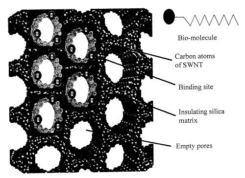
Fig. 4 shows schematically an MCM-41 catalytic template with pores of uniform
diameter arranged in a closely spaced two-dimensional (hexagonal) pattern. As
mentioned above, the walls between pores can be as thin as 0.6-0.8 nm for pore
diameters of between 1 mn and several ten nm. This allows dense packing of the
SWNT. As seen in Fig. 4, several of the pores are each filled with a SWNT,
with the
black circles schematically depicting individual carbon atoms. The free ends
of the
SWNT are shown as projecting out from the major surface of the template and
being
functionalized with receptor sites A (A = biotin) that are adapted to
selectively bind
with target ligands A' (A' = monoclonal antibiotin). The exemplary ligands and
receptors demonstrate a reversible reaction and specificity, for example, over
bovine
immunoglobulin. The use of MCM nanotube arrays is ideal for this application,
because one can create multiple redundant sensors that can be produced to
counteract
fouling by the biological molecules which are much larger than the tip end of
a
SWNT, andJor create multiple selectivity for different absorbed receptors.
Since the
22
CA 02470946 2004-06-17
WO 03/052182 PCT/US02/41030
tubes are open-ended and retained in the catalytic template, they are not at
risk of
being damaged during functionalization.
The presence of molecules at binding sites can, for example, be detected
optically. Figs. SA- SC show the electronic band structures of a simpler
system,
namely a SWNT (10,0) which is expected to be metallic (Fig. SA), a NOZ
molecule
(Fig. SB), and the combined SWNT-N02 system (Fig. SC). Arrows indicate the
occupied states of NOZ molecular orbitals. The optical transition from the
uppermost
occupied state of the NO2 molecular orbital in the SWNT to the unoccupied
higher
energy conduction band can be detected.
As mentioned above, the ends of the SWNT can be provided with ohmic
contacts. The electrical characteristic of the SWNT can be altered, for
example, by
attaching a receptor site between contacts, creating a field effect transistor
(FET).
The FET can be effective in amplifying signals induced by the presence of the
target
molecules (ligands). In a conventional FET, current flows along a
semiconductor
pathway called a channel. The olnnic contacts of the SWNT form the source and
the
r
drain at the ends of the channel. The presence of the ligand changes the gate
voltage
and hence the effective electrical diameter of the channel. A small change in
gate
voltage results in a significant variation in the current from the source to
the drain.
Nanoscale FET's can be have an increased sensitivity due to the greater
surface
(gate) to volume (channel) ratio, malting single molecule sensitivity
possible. These
devices are reversible by removing the ligand.
23
CA 02470946 2004-06-17
WO 03/052182 PCT/US02/41030
Nanoscale transistors
Unlike MCM-41 which has substantially parallel one-dimensional pores
arranged in a two-dimensional pattern, as depicted in Fig. 4, MCM-48 has a
cubic
pore system arranged in a three-dimensional interconnected networlc. As in MCM-
41, tetrahedrally coordinated Si can be replaced by metals from the first row
of
transitional elements, such as Ti, V, Cr, Mn, Fe, Co, and Ni, as well as other
metals
known in the art., e.g., Al, Zr and Mn. Since pores extending in the MCM-48
framework in different directions can overlap, crossbar switches and Y
junction
transistors are feasible. Since the SWNT can be grown in the pores of the MCM-
48
catalytic template with controlled physical and electronic properties by
employing
the template preparation and SWNT growth methods described above, the crossbar
switches and Y junction transistors can also have predictable and selectable
electronic transport characteristics.
Fig. 6A shows schematically a three-dimensional configuration of SWNT
forming a crossbar switch that can be grown inside a MCM-48 framework.
Exemplary SWNT 61 and 64 cross each other so as to make electrical contact.
Contacts 62, 63 can be placed at end sections of SWNT 61, and at least one
contact
65, 66 can be placed at end sections of SWNT 64. Current can flow between SWNT
61, 64, or current flow along one of the SWNT 61, 64 can be controlled by
applying
an electric potential to the other SWNT 64, 61, for example, at one of the
contacts
62, 62, 65, 66. In another exemplary embodiment depicted in Fig. 6B, the SWNT
67
terminates along SWNT 61, forming a Y junction transistor similar to an FET.
24
CA 02470946 2004-06-17
WO 03/052182 PCT/US02/41030
Current flow through SWNT 61 between contacts 62, 63 can be controlled at
junction 69 by applying a gate voltage to contact 68 formed on SWNT 67. The
carbon nanotube networks formed inside the MCM-48 have proven to be strong
enough to survive removal of the framework, for example, by etching in HF. For
operation, these devices can hence remain either inside the frameworlc with
only the
ends of the nanotubes exposed for contact formation, or the devices can be
first
individually functionalized with contacts and then removed, from the
frameworlc. It
will be understood that the illustrated embodiment of a Y junction transistor
is only
exemplary and that entire integrated circuits that include semiconducting SWNT
transistors, switches and/or metallic SWNT interconnects can be formed inside
the
different types of frameworks described above, with the physical and
electronic
properties of the SWNT determined by the selected pore size of the framework
and
the wall chemistry. Such integrated circuits can perform functions presently
executed
in semiconductor devices, for example, computational and logical operations
and
memory functions.
While the invention has been disclosed in connection with the preferred
embodiments shown and described in detail, various modifications and
improvements thereon will become readily apparent to those skilled in the art.
For
example, ordered arrangements of mesoporic pores suitable for the controlled
growth
of SWNT can also be prepared by magnetically orienting different Fe-doped
layer in
different directions by polarization in an external magnetic field during the
growth
phase. If Fe or another magnetic material is incorporated in the SWNT, nano-
CA 02470946 2004-06-17
WO 03/052182 PCT/US02/41030
magnetic junctions can be formed that can be responsive to an externally
applied
magnetic field or to a magnetic field generated by electric currents flowing
through
proximate nanotubes. MPMS catalytic templates for nanotube growth can also be
prepared as aligned crystals on quartz plates and/or Si wafers. Accordingly,
the spirit
and scope of the present invention is to be limited only by the following
claims.
What is claimed is:
26