Note: Descriptions are shown in the official language in which they were submitted.
CA 02471231 2004-06-18
POWER FACTOR CONTROLLER
FIELD OF THE IN VENTION
The present invention relates to an electronic power supply and more
particularly to a power factor controller or corrector (PFC). This invention
is related
to U.S. Patent No. 5,357,418 issued October 18, 1994 ofthe same inventor,
which
concerns a hybrid power supply with improved regulation.
BACKGROUND OF THE INVENTION
Presently known PFCs have the following drawbacks:
They use a double 'Feedback loop, i.e. one to sense the line current and the
other to sense the output voltage. This arrangement requires heavy calculating
power
in the chips that generate the driving pulse width to the power FETs;
These chips have important Limitations that end up in incoherent system
equations for calculations of the chokes and power FETs characteristics, thus
requiring a lot of empirical testing from the designer or trouble shooter.
Besides, it
still remains unclear whether these chips are usable above 500 watts. All
these factors
lead to very substantial development and maintenance costs.
This is probably the major reason why the U.S. Government has been
reluctant to adopt the IEC 555-2 norm for the last decade.
An objective ofthe invention is to eliminate the above deficiencies and
provide a simple system allowing use of a single basic equation and to
increase
predictability of the circuitry.
CA 02471231 2004-06-18
WO 03/058797 PCT/CA03/00009
Another objective of the invention is to provide a system which is applicable
to any power output (watts to kilowatts).
SLfMMARY OF THE I1~VENTION
In essence, the power factor controller or corrector of the present invention
comprises separating load and line regulations in the powex supply circuit and
providing a 1/x2 modulator module for the line regulation in which switching
frequency is inversely proportional to the square of the line voltage.
Furthermore, the
load regulation is preferably achieved by a 1/v pulsewidth generator which
generates
a pulse duration that is inversely proportional to the voltage from a
differential gain
circuitry that produces a control voltagewhich is proportional to the
difference
between a fraction of output voltage and a fixed reference voltage. Also, a
loop delay
may be provided between the differential gain circuitry and the 1/v pulse
generator.
The power factor controller of the present invention may be advantageously
combined with a hybrid power supply, such as disclosed and claimed in U. S.
Patent
No. 5,357,418 and having a 1/x frequency modulating module. The combination
comprises cascading the 1/x2 module with the 1/x module.
According to the present invention, the PFC boost circuit will exhibit the
following properties:
The AC line current will be sinusoidal, i.e. will look like the AC line
voltage,
thus bringing the power factor close to 1 and the harmonic content of AC
current will
be close to 0. Such characteristics would meet IEC 555-2 requirements and
other
subsequent IEC norms;
The output DC voltage will be about 450 VDC for AC line variations from 85
VAC to 265 VAC.
-2-
CA 02471231 2004-06-18
WO 03/058797 PCT/CA03/00009
Shown input/output relationship represents a theoretical view on the present
power factor corrected power supplies.
BRIEF DESCRIPTION OF DRAWINGS
In the appended drawings:
~ Fig. 1 shows a previously used electronic power supply which is neither
regulated nor PFC controlled;
Fig. 2 shows a block-diagram of the PFC control system of the present
invention;
Fig. 3 shows an electronic circuitry illustrations of block-diagram of Fig. 2;
Fig. 4 shows a cascade arrangement of module of the present invention with
module of U.S. Patent No. 5,357,418.
Fig. 5 shows a diagram of voltage/current phases of the present invention;
Fig. 6 shows a diagram of voltage%urrent phases of known power supply
systems which are not PCF controlled.
DETAILED DESCRIPTION OF THE INVENTION
An electronic power supply can be defined as a power converter converting
AC line voltage ( 115 VAC or 220 VAC) into a DC voltage necessary to feed any
electronic circuitry. The simplest electronic power supply is shown on Fig. 1
and
includes a very primitive transformer (TR), rectifying bridge (BR) of
capacitor (G)
type. However, such a simple arrangement is seldom used due to'the following
reasons:
~ output DC voltage will change whenever the line voltage changes, thus not
providing any reliable line regulation;
-3-
CA 02471231 2004-06-18
WO 03/058797 PCT/CA03/00009
~ even if the Line voltage is stable, DC voltage will change if current is
drawn
by the load changes, thus not providing any load regulation;
~ at 60 Hz, weight and size of transformer will become prohibitive;
~ capacitor charging and discharging will produce a high peak current
demands, i.e. harmonics of 60 Hz. Such generation of harmonics was tolerated
until
January 1-, 2001, but is ~o longer tolerated in Europe and soon will not be
tolerated in
North America.
The above deficiencies are particularly addressed by the system of the present
invention. Electronic industry needs power supplies having much better
performances
than the circuit shown in Fig. 1 can offer, since modern power supplies are
much
more complex.
The typical power supply users will expect their electronic power supply to
fulfill not only one but all of the following conditions:
~ high quality regulations;
~ high efficiency;
~ small size and weight;
~ high power factor.
High quality regulations means that:
~ generated output voltage essentially does not change when line voltage or
Ioad changes (typically less than 0.1%);
~ no noise is essentially superimposed on the output voltage (typically less
than 1 millivolt);
~ output impedance of the supply is negligible (typically 10 milliohms);
~ transient response is fast (typically 10 microseconds).
-4-
CA 02471231 2004-06-18
WO 03/058797 PCT/CA03/00009
Effects of low quality regulations are:
~ Output voltage varying too much, which is not too critical for digital
circuitry, but is very annoying for analog circuitry such as timers, A/D
converters,
multipliers, integrators, etc.
S ~ Noise will randomly trigger flip-flops and provoke intermittent and
unexpected breakdown in digital circuitry;
~ Transient response is too low and severely limits the frequency response of
user's power circuitry, such as power amplifiers, plasma electrodes, etc.
High eff ciency means the following:
I O ~ All power which is not used in the load is going to generate heat in the
power supply of the user's circuitry. In the past, 7S% to 80% e~ciency was
considered to be acceptable, but in the future, it may be insufficient in view
of the
following reasons:
~ simple mathematics show that a power supply having 7S% efficiency will
15 heat up not 20%, but 500% more if compared with a 9S% efficiency power
supply;
~ there is a strong correlation between e~ciency and other parameters, such as
size, weight, noise content and reliability.
Effect of poor efficiency is:
Above all, loss of reliability, which is a highly non-linear function of
20 temperature. If temperature increases 10°C, MTBF decreases several
times.
Small size and weight means the following:
At the present time, size/weight proportions are about 2-3 cubic inches /1 lb
(70-100 cubic cm/1 kg) per regulated I watt produced. The proportion could be
even
more if the user can handle the heat dissipation problem with which he does
not feel
-5-
CA 02471231 2004-06-18
WO 03/058797 PCT/CA03/00009
comfortable unless he is a heat transfer expert.
High power factor means the following:
Power supply should consider the hydro line as a pure ohmic resistor, i.e.
current drawn from the grid is sinusoidal with less than 3 amps of harmonic 3
content. Ideally, the power factor should be around 99%. However, nearly all
power
supplies designed before 1990, and quite a few now have a power factor of
around
66%.
Effect of poor power factor is:
Non-compliance.with IEC 555-2 norm issued in 1990, which is compulsory in
Europe since January 1, 2001, and is expected to become compulsory by the CSA
(Canadian Standard Association) in 2002 and in the U.S. in 2003.
Present state of the art:
Major power supply makers (Kepco, Lambda, Power One, Acopian, etc.)
might satisfy one or two of the above four factors, but none of them satisfy
aI1 four.
This may be explained as being due to the following problems:
Satisfying all four factors together is extremely difficult due to conflicting
requirements between efficiency and quality of regulations;
Paradoxically, power supply development has been considered for a long time
a non-glamorous technology and relatively little R&D has been done when
compared
with the field of communications and computers.
In view of the above, the user still has to choose between bad regulation and
efficiency with some risk of malfunctions always present. Cost of regulated
supplies
has not come down, like the rest of electronic gear. A custom power supply of
average complexity can take more than 1 year of development and cost around
-6-
CA 02471231 2004-06-18
WO 03/058797 PCT/CA03/00009
$200,000. Some recent special 1 kw power supplies development had taken 5
years
and 1. S million dollars.
The PFC controller of the present invention was designed with a view of the
following factors:
S ~ to satisfy impending compulsory PFC requirements for all power supplies
above 300 watts in view of IEC SSS-2 and other IEC norms;
~ need for PFC for 5 kilowatts power supply for plasma electrodes;
~ failure to find a reliable design information and off the-shelf chips for
power
above S00 watts;
~ knowledge of tremendous difficulties of developers to achieve PFC at only 1
kilowatt;
~ finding that some principles used in U.S. Patent No. S,3S7,418 could also be
used for the system of the present invention, such as clear separation of line
and load
regulations and hyperbolic modulations.
1S The PFC controller of the 'present invention uses the same philosophy as
U.S.
Patent No. S,3S7,418 clearly separating the line regulation (open loop) from
the load
regulation (closed loop). This feature allows the use of a single basic
equation and to
increase predictability of the circuitry. Such approach is general and may be
applicable to any power output (watts to kilowatts).
It can be shown both mathematically and experimentally that the power output
of the basic boost circuitry of Fig. 1 is:
P-KF~(PW-)2
L
Wherein:
_7_
CA 02471231 2004-06-18
WO 03/058797 PCT/CA03/00009
P is wanted output power in watts;
K is constant;
F is frequency of switching of power FETs in kilohertz;
V is line RMS voltage in volts;
PW is pulsewidth in microseconds;
L is value of power inductance in millihenries.
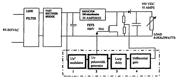
Referring now to Fig. 2 of the drawings which shows a block-diagram of the
PFC controller of the present invention, it provides the following:
Line regulation step
. For a given constant power, if line varies for example from 1 lOv to 220v
(factor of 2), choke will tend to force four times more power into the load by
raising
output DC voltage two times. To prevent this, frequency has to be decreased
four
times. Consequently, switching frequency has to be inversely proportional to
the
square of the Iine voltage. This process is achieved by block 1 representing
1/x2
modulator which is assigned to regulate the line variations. It produces a
frequency
proportional to the inverse of the square of the line voltage. For example, if
the line
voltage is 115 VAC, frequency generated by block 1 will be 80 kilohertz. If
the line
voltage is 230 VAC, frequency generated by block 1 will be 20 kilohertz.
Load regulation step
In case the load demand varies abruptly, for example from S KW to 0 watts,
choke will tend to force SKW into an open circuit, which will raise the output
voltage
to infinity if pulsewidth is not decreased rapidly to about 0 microseconds. In
other
words, pulsewidth has to be decreased very fast when output voltages increase.
Block 2 represents a 1/v pulsewidth generator which will generate a pulse
_g_
CA 02471231 2004-06-18
WO 03/058797 PCT/CA03/00009
duration which is inversely proportional to V, wherein V comes from
differential gain
represented by block 4. Block 4 produces a control voltage which is
proportional to
the difference between a fraction of the output voltage and a fixed reference
voltage.
Loop delay represented by block 3 is analogous to a time lag circuitry used in
analog control loops, such as Bode or Nyquist criterion techniques.
In conclusion, block 1 is provided fox line regulation and blocks 2, 3 and 4
are
provided for the load regulation. For example, if the load varies from 5
kilowatts to 0 .
kilowatts (open circuit), pulsewidth will vary from 5 microseconds to 0
microseconds.
Fig. 3 shows a preferred embodiment of the circuit representing blocks 1-4 of
Fig. 2 which are operating in the following manner:
U3 of block 1 is a simple logic CMOS standard (CD 4007) dual
complementary pair plus inverter logic gate used for its analog properties.
This chip
contains one P-channel FET and one N channel FET which can be used as a non-
linear voltage controlled resistor. When connected to inverters of the same
chip
through R9, R10 and R11, a non-linear voltage controlled oscillator is formed,
the
frequency of which can be made varying like the inverse of the square of the
control
voltage applied to pin 3 of U3. Pin 12 of U3 outputs a varying frequency which
is
applied to U4 of block 2, which is a standard CMOS (CD4047). U4 is producing
fixed duration pulses 100 nanoseconds wide. These short pulses are applied to
US
FET driver (TC 427) which puts element Ql (IRFZ40) of block 2 "ON" in about 30
nanoseconds. Whenever Ql conducts, capacitor C1 of block 2 is discharging in
about
100 nanoseconds for each period of the frequency produced by U3. Whenever
pulse
from U4 is low, Q1 is "OFF" and C1 starts to charge up as a ramp due to a
constant
-9_
CA 02471231 2004-06-18
WO 03/058797 PCT/CA03/00009
current applied by Ul of block 2 current source. Voltage of Cl is applied to
input 1 of
U6 comparator of block 2. Input 2 of the comparator U6 receives a varying DC
reference produced by element US of block 4. Whenever voltage at C1 reaches
the
value of the DC reference, comparator U6 switches to a logic "1" state. With
subsequent proper gating, net result is a pulse of duration proportional to
the voltage
coming from pin 1 of U8 and is occurnng at each period of frequencies produced
by
U3.
Voltage appearing on the load side is firstly divided in block 4 into 7.8 VDC
corresponding to 350 VDC and 10 VDC corresponding to 450 VDC. Difference
between this voltage and a fixed reference voltage of 10 V is amplified by a
factor of
4.7. Thus, if 10 VDC corresponding to 450 VDC appears at divider, output pin 1
of
U8 will be "0" V. This will produce a pulsewidth of 0 microseconds at U6, i.e.
no
energy will be transferred to the load. In this case, a voltage of 450 VDC at
the load
means that the circuit is open. In case the voltage at the divider is 7.8 VDC
corresponding to 350 VDC as full load situation, output at pin 1 of U8 will be
maximum, and subsequently, pulsewidth produced at U6 will be maximum, thus
allowing transfer of energy to the load and increasing the output voltage back
to 450
VDC. Practically, loading process will not vary so abruptly as "no load" -
"full load",
and pulsewidth will be adjusted by control loop continuoulsy and slowly. In
this case,
variations from "no load" to "full load" (or the reverse) occurs only at start-
up or
when the load is accidentally removed (for example, broken connection).
Feedback
loop will react in both cases, but with some transient effect. Following
regulation
stages will absorb this transient effect. Such basic principle is valid even
in the case
of abrupt variations. In view of this fact, pulse width will be adjusted by
control loop
-10-
CA 02471231 2004-06-18
WO 03/058797 PCT/CA03/00009
in any loading circumstances. Elements of block 3, such as R19, C8 and buffer
will
introduce some delay in the in loop in order to avoid oscillations. The buffer
of block
3 comprises amplifier Lm324/2 element, wherein pin 7 strapped to pin 6
provides
infinite input impedance at pin S and near "0" output impedance at pin 7.
S It should be emphasized that the PFC system of the present invention could
be
used with any "boost circuitry" whose requirements could be stated as follows:
Output should be a high value (450V to 1000V) regulated DC voltage. Boost
circuit can output DC voltage several times higher than the peak voltage;
Input should look to the grid line (110 VAC, 220 VAC, SSO VAC, etc.) like a
pure ohmic resistor;
The current drawn should be pure sinusoid (see Fig. S), in phase with the AC
line voltage. The voltage/current relationship shown in Fig. S is present in
any PFC
controlled power supply, including that of the present invention.
In contrast, Fig. 6 shows a configuration of the current line which is not
useful
1 S for the PFC system of the present invention. It is normally present in any
power
supply that has no PFC. The high peak currents of this configuration produce
problems in the hydro lines.
All electronic components shown on Fig. 3 represent a preferred embodiment
only and had been chosen mainly due to their immediate availability. Any other
equivalent elements could be used to provide the same function for the same
result.
Fig. 4 represents an arrangement according to U.S. Patent No. S,3S7,418 in
combination with the PFC controller of the present invention. When cascading
one
1/x2 PFC module of the present invention and one 1/x module of the U.S. Patent
No.
S,3S7,418, as shown in Fig. 4, it is possible to realize, for example, a 0-
100V, 10
-11-
CA 02471231 2004-06-18
WO 03/058797 PCT/CA03/00009
amps (1 kilowatt) adjustable regulated power supply.
In this case, the combined performance will be:
Regulation: linear grade, i.e. line + load of 0.01%; transient response - 20
microseconds and output impedance - 20 milliohms;
Ripple + noise of 1 millivolt peak to peak;
Efficiency: 92.5%;
Power factor: 99%;
Size and weight: 500 cubic inches, 10 Ib (2w/cubic inch,100w11b).
Presently available "linear type" regulated power supplies have the following
characteristics:
Regulation: linear grade, i.e. line + load of 0.01%, transient response - 20
microseconds, output impedance - 20 milliohms;
Ripple + noise: 1 millivolt peak to peak;
Effciency: 30-40% (2 kilowatts of heat to dissipate internally);
Power factor: 66%;
Size and weight: 2000 cubic inches, 100 Ib (0.5 w/cubic inch, 10 w/lb)
Presently available "switching type" regulated supplies have the following
characteristics:
Efficiency: 75% (250 watts of heat to dissipate internally);
Power factor: 99%;
Size and weight: 500 cubic inches, l2 lbs (2 w/cubic inch, 80 w/lb)
Regulation: line + load of 0.1%, 0.5%, transient response - 2000 to 5000
microseconds, output impedance - unknown;
Ripple + noise: 150 millivolt peak to peak.
:12-
CA 02471231 2004-06-18
WO 03/058797 PCT/CA03/00009
In view of the above data, in the presently available regulated power
supplies,
the customer has to make a difficult choice between a well regulated, but very
hot
power supply and a cool, but badly regulated power supply. In practice, the
customer
has to pick the lesser of two evils; ~ liut always will have non-negligible
risks.
Separate PFC modules do exist, which will deliver 450 VDC outputs, but the
customer is left with the problem of converting the 450 VDC to lower voltages.
Usually, he adds a switching supply in cascade, which is likely double the RFI
output.
Besides, such modules axe not currently available above 500 watts. Such
technology
is not very mature even in Europe.
Other advantages of cascading shown in Fig. 4 allows to decrease the
development costs of power supplies by a factor of 10 considering the fact
that
development cost of a medium complexity power supply is about $250,000 with
the
development time of 18 months. This factor reflects the sale price, since a
typical
price for a well regulated 1 KW power supply is $5000.00.
1S The reason for such excessive costs is the fact that most technologies used
up
to date do not separate the line regulation and the load regulation. Having
lines
varying by factor of four (85 VAC - 265 VAC) and load varying by a factor of
infinity
(0 watts to 1 kilowatt) make the performance of the feedback loop almost
unpredictable, especially since complex magnetic components, such as high
frequency transformers and chokers, are in the feedback loops. Net result is
that
numerous iterations and breadboards have to be built before wanted
performances are
achieved. In this case, magnetic components very often have to be designed by
cut
and try guesswork. It all results in expensive debugging time when testing the
circuitry.
-13-
CA 02471231 2004-06-18
WO 03/058797 PCT/CA03/00009
As a conclusion, it is clear that separating load and line regulation used in
the
present invention makes analysis coherent and predictable. In this case,
equation for
determining values of components; especially magnetic components, are
numerous,
but easily implemented on an Excel spread sheet.
As a result, cascade arrangement of Fig. 4 is the most commercially
advantageous for realizations of regulated electronic power supplies, which
represent
probably over 90% in the market of all power supplies.
A similar, or at least very close arrangement, may be used for efficient, high
power battery chargers (kilowatts), e~cient, high power current sources
(kilowatts)
and efficient, high power sinewave inverters (kilowatts).
-14-