Note: Descriptions are shown in the official language in which they were submitted.
CA 02471268 2005-09-01
Official Title: METHOD FOR THE PRODUCTION OF AN
ELECTRICALLY CONDUCTIVE RESISTIVE LAYER AND
HEATING AND/OR COOLING DEVICE Description
The invention at first covers a method to produce an electrically conductive
resistance layer on which an electrically conductive material will be applied,
by
means of thermal spraying, to a non conductive substrate.
Such a method is already known from the DE 198 10 848 Al patent. This patent
describes a heating element which is produced by applying on the surface of a
substrate through a plasma-spray method or an electrical arcing method band-
shaped layers of an electrical conductive and resistance creating material. To
achieve the desired shape of the electrical conductive layer, a separation
layer is
applied first to the substrate by means of a printing method. The separation
layer
is from such a material that, it does not bond with the electrically
conductive layer
on those parts of the substrate where it is present.
The known method has the disadvantage that it is relatively complex and
therefore the parts with the electrically conductive resistance layers are
comparably expensive. In addition to this, only more or less level surfaces
can be
covered with an electrically conductive layer.
The invention at hand therefore is to further develop the previously described
method in a way that the production of a substrate with an electrically
conductive
layer can be performed more easily and cheaper and that also complex-shaped
objects can be applied with an electrically conductive resistance layer as
well.
This task is accomplished through a method in the initially mentioned art by
applying the electrically conductive material to the surface of the substrate
in
such a manner so that the applied material layer at first does not necessarily
show the desired shape but that later the material layer will be taken-off in
a way
1
CA 02471268 2006-10-18
that an electrically conductive resistance layer is created which in
essentially shows the
desired shape.
For the invented method no special pre-treatment is necessary to get to the
desired
shape of the electrically conductive resistance layer. Instead the
electrically conductive
material from which forms the resistance layer consists is surface-applied
essentially
evenly to the electrically non-conductive substrate. The application through
thermal
spraying cares for the high adhesion of the electrically conductive material
to the
electrically non-conductive substrate. In addition, different materials can be
applied
quickly and very evenly in this way to the electrically non-conductive
surface.
After that, the electrically conductive material will be taken-off with an
appropriate
device from certain areas. In this way, even complex shaping of the
electrically
conductive layer is achieved in only 2 work-steps.
In one embodiment, the present invention provides for a heater adapted for
fixed
placement proximate a separate and external part or medium to be heated and
defining a shape commensurate with the part or medium to be heated, the heater
comprising: a complex shaped substrate; a nonconductive layer formed over the
substrate; an electrically conductive resistive layer formed on the
nonconductive layer
by a process of forming a material onto the nonconductive layer and
subsequently
and selectively removing areas of the material using a laser such that no
residue
remains on the nonconductive layer to increase an insulation effect of the
nonconductive layer, wherein removing areas of the material creates a desired
resistance of the electrically conductive resistive layer and the electrically
conductive
resistive layer defines a meander pattern after removing areas of the
material.
In another embodiment, the present invention provides for a heater adapted for
fixed
placement proximate a separate and external part or medium to be heated and
defining a shape commensurate with the part or medium to be heated, the heater
comprising: a complex shaped substrate; and an electrically conductive
resistive
layer formed on the complex shaped substrate by a process of forming a
material
2
CA 02471268 2006-10-18
onto the complex shaped substrate and subsequently and selectively removing
areas
of the material using a laser such that no residue remains on the complex
shaped
substrate to increase an insulation effect of the complex shaped substrate,
wherein
removing areas of the material creates a desired resistance of the
electrically
conductive resistive layer and the electrically conductive resistive layer
defines a
meander pattern after removing areas of the material.
Advantageous additional features of the invention are stated in sub-claims.
It is proposed that first the material layer be removed from certain areas by
means
of a laser beam or a water jet or a powder sand blast.
Using a laser beam, the material will be greatly heated which causes it to
evaporate.
The use of a laser has the advantage that very quickly very high doses of
energy can
be brought to the electrically conductive material so that it immediately
evaporates.
Due to the instant evaporation of the electrically conductive material it is
assured that
only relatively little heat will be brought to the surface which lies
underneath the
electrically conductive material. That surface will not be damaged by the
method
contained in this invention. The evaporation has - compared to burning - the
advantage that generally no residues remain on the surface of the evaporated
areas
which makes their insulation effect very good.
With the appropriate optics of the device which sends out the laser beam the
beam
can be directed in an almost unlimited way to the subject. Therefore randomly
complex contours can be evaporated from the electrically conductive material
so that
correspondingly complex electrical resistance layers can be manufactured. In
addition even such subjects which themselves are complex three-dimensionally
shaped can be worked-on. Therefore, an electrically conductive resistance
layer of
complex geometry can be manufactured in only two work-steps.
2A
CA 02471268 2006-10-18
Using a water jet will bring no thermal energy to the subject at all. This is
especially
advantageous when treating heat sensitive plastics. The same is applicable
when
utilizing powder sand blasting.
In another especially preferred further development of the invention it is
proposed that
during the removal of the material layer the electrical resistance of the
electrically
conductive resistance layer is at least indirectly obtained. This way a
precise quality
control is immediately possible during the production of the electrically
conductive
layer.
2B
CA 02471268 2004-06-21
In further development to this it is proposed to compare the actual resistance
value of the electrically conductive resistance layer to a set value and to
reduce
the difference between set value and actual value by additional removal of the
electrically conductive layer. This has the advantage that already during
production of the electrically conductive layer deviations from the desired
resistance can be adjusted.
Such deviations can be created for example when during spraying of the
thermally conductive material inconsistent amounts of the electrically
conductive
material are applied to some areas of the surface in a way that in those areas
the
thickness of the electrically conductive layer gets to a different thickness
than in
other areas. With the proposed method deviations of the actual value to the
set
value can be adjusted up to a precision of +/-1 %. The additional removal of
zones
of electrically conductive material can either imply a shortage or an
elongation of
the electrically conductive layer and/or it can imply a change in the width of
the
electrically conductive layer.
Herewith it is again especially advantageous when the collection of the actual
value of the electrical resistance of the electrically conductive resistance
layer
and reduction in the difference between the actual value and the set value is
being done simultaneously. This is possible, because already during the
processing of the electrically conductive layer with a laser beam the
electrical
resistance value of the electrically conductive layer can be measured. If this
method is applied during production of the electrically conductive layer time
and
consequently money can be saved.
In an embodiment of the method according to the invention it is proposed that
the
material-layer be removed in such a way that at least at one spot of the
electrically conductive layer, an intended melting spot is created that
functions as
the melting fuse. Such an integrated melting fuse increases the electrical
safety
of the electrically conductive resistance layer. That way the melting fuse can
be
incorporated into the electrically conductive layer practically without any
additional cost and expenditure of time.
It is also advantageous, when the material layer is removed in such a manner
that the electrically conductive resistance layer at least in some areas has
the
shape of a meander. This enables the creation of a possibly long electrically
conductive layer on a small area.
It is also proposed that after the removal of some areas of the electrically
conductive material and the completion of the electrically conductive
resistance
layer, the layer be applied by an electrically non-conductive intermediate
layer.
Next on top of the intermediate electrically non-conductive layer another
electrically conductive layer can be thermal sprayed in such a way that it
essentially does not show the desired shape yet. After this, using a laser
beam
the material layer will be removed in some areas so a second electrically
conductive layer is created which has the desired shape. The invention allows
therefore the use of several layers on top of each other. It must be noted
that the
invention not only covers an application with two electrically conductive
3
_......W,_...r,.......~....._..._. . _
CA 02471268 2004-06-21
resistance layers but also is applicable to any desired number of arranged
resistance layers.
The electrically conductive material comprise preferably Bismuth (Bi),
Tellurium
(Te), Germanium (Ge), Silicon (Si) and/or Gallium Arsenite. These materials
proved to be well suitable for thermal spraying and the following treatment
with
laser beams. Furthermore, with these materials the known pertinent technical
effects are realizable.
Well suitable for applying electrically conductive materials on the substrate
are
plasma-spraying, high speed flame spraying, arc spraying, autogenious
spraying,
laser spraying or cold gas spraying.
Furthermore it is proposed to apply the electrically conductive material and
to
remove the material layer in certain areas and that such a material is used in
a
way that an electrical heating layer or an electrical cooling layer is
created. In the
production of an electrical cooling layer the "Peltier effect" is beneficially
used.
One further beneficial embodiment is proposed so that the local electrical
resistance of the electrically conductive resistance layer will be adjusted by
means of local heat treatment. Through heating local oxides can be brought
into
the layer, which affects the local electrical conductivity of the material.
This
makes a specially precise and fine tuning of the electrical resistance
possible.
It is also beneficial when the electrically conductive layer gets sealed. This
is
especially advantageous on porous substrates (for example metal with an
intermediate layer of AI2O3). Sealing decreases the risk of electrical
sparking due
to moisture especially at high voltages. Suitable materials to seal the
surface are
Silicone, Polyimide, soluble Potassium or soluble Sodium. They can be applied
through plunging, spraying, painting etc. The tightness of the seal is best
when
the sealing layer is applied under vacuum.
Electrically non-conductive substrates can also be glass or glass-ceramics.
The
electrically conductive resistance layer can be plasma-sprayed to these
materials
durably. Due to the good electrical insulation of glass it is unnecessary to
ground
the resistance layer. Also possible is the use of special high temperature
glass
such as for example Ceranglas .
The invention also applies to a heating- and/or cooling device with a non
conductive substrate and an electrically conductive resistance layer which is
thermally sprayed on the substrate.
Manufacturing cost for such a heat- and/or cooling device can be reduced when
the resistance layer envelops an electrically conductive material, which is
surface-applied through thermal spraying and then removed by a laser beam
from certain areas and brought into the desired shape.
Next especially preferred embodiments of the invention illustrate design
examples of the invention with reference to the attached drawings.
The drawings display:
4
...........
,.--_
CA 02471268 2004-06-21
Figure 1 a perspective layout of a tube on which an electrically conductive
material is sprayed-on
Figure 2 the tube of Fig.1. It's electrically conductive layer is worked-on
with
laser beams
Figure 3 a side view of the tube of Fig. 2 after completion
Figure 4 the top view on a plate-shaped part with a meander-shaped
electrically
conductive resistance layer
Figure 5 two diagrams. One shows the progression of time of the electrical
resistance and the other shows the progression of time of the length of the
electrically conductive resistance layer from Fig. 4 during manufacturing; and
Figure 6 shows a section through the plate-shaped part with 2 electrically
conductive resistance layers arranged one above the other.
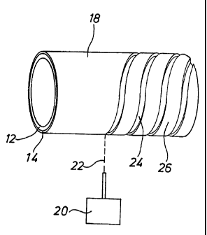
Figures 1 and 2 show the production of a tube shaped flow heater. On a high
temperature resistant tube (12) with an electrically non-conductive material
an
electrically conductive layer is applied (Fig.1). The application is conducted
by
means of a device (16) which is used to spray particles of Germanium (Ge) (18)
on the tube (12). In this case, cold-gas-spray method is used.
In the spraying process the unmolten particles of Germanium (Ge) are
accelerated to speeds of 300 - 1200 m/sec and sprayed on to the tube (12). On
impact the Ge-particles (18) as well as the surface of the tube get deformed.
Because of the impact surface-oxides of the surface of the tube (12) get
broken-
up. Through micro-friction because of the impact the temperature of the
contact
area increases and leads to micro-welding.
The acceleration of the Ge-particies (18) is done by means of a conveyor-gas
whose temperature can be slightly increased. Although the Ge-powder (18) never
reaches its melting temperature, the resulting temperatures on the surface of
the
tube (12) are relatively moderate so that for example the tube can be made
from
a relatively cheap plastic material.
In other, not displayed construction examples, methods other than cold-gas-
spraying can be used such as plasma-spraying, high-speed-flame-spraying, arc-
spraying, autogenious-spraying or laser-spraying to apply the electrically
conductive material to the substrate. Instead of Germanium (Ge), also Bismuth
(Bi), Tellurium (Te), Silicon (Si) and/or Gallium Arsenide can be used,
depending
on the desired technical effect.
The coating of the tube (12) with particles of Germanium (Ge) is done at first
in a
way that bit by bit the entire surface of the tube (12) is covered with the
Germanium-layer (14) (compare Fig. 1). This material layer however does not
have the desired shape yet: To be able to manufacture a tubular shaped flow
heater an electrically conductive resistance layer must be produced which
CA 02471268 2004-06-21
surrounds the tube (12) in a circumferential direction in a spiral shape. To
achieve this, as can be seen in Fig. 2, a laser beam is directed to the
"unshaped"
material layer in a way that a spiral-shaped area (24) around the tube (12) is
created in which the sprayed-on electrically conductive material (14) is not
present any more.
This is achieved by having the material in the material layer (14) met with
the
laser beam so that it heats and immediately evaporates that part of the layer
(14).
The laser device on one side and a - in the figure not shown - device which
holds the tube (12) is one the other so that a continuing work process by the
laser
device (20) is possible.
As can be seen from Fig. 3, an electrically conductive layer (26) is created,
that
stretches spirally from one axial end of the tube (12) to the other. The flow
heater
(28) is formed by the electrically conductive resistance layer (26) and the
tube
(12).
In Fig. 4 a flat heat plate (28) is shown from a top view. This consists of a -
in this
view not visible - non conductive substrate on which, analog to the described
process of Fig. 1 and 2 at first a sheet-shaped layer of material (14) gets
applied,
out of which certain areas (24) are being evaporated with a laser beam (for
simplicity only one area (24) was marked). Hereby a meander shaped
electrically
conductive resistance layer (26) was created that stretches from one end of
the
plate (28) to the other. This, however, has two specialties: On the upper end
of
Fig. 4 the material layer (14), from which the electrically conductive layer
was
produced, was evaporated in a way that the conductive track (26) shows a
narrowed section. This creates a melting fuse (30) in such a way that the use
of
the heater plate (28) is protected.
The second specialty is that the heating capacity or as the case may be the
density of the heat flow was corrected during manufacturing that it
corresponds to
the desired heat capacity or as the case may be the desired heat flow to very
high precision. This is achieved as follows: A voltage is applied to the ends
32
and 34 of the electrically conductive resistance layer (26) during the
evaporation
process so that the electrical resistance of the electrically conductive layer
(26)
can be measured continuously. The material layer (14) will be evaporated by
the
laser beam at first in only small sections (24). The horizontal layers of the
evaporated areas (24) of Fig. 4 stretch only from a corner (dashed lines) (36)
to
the horizontal corner (38) of the electrically conductive layer (26) which
lies above.
(Also here because of illustration purposes only one area (24) is shown). In
addition to this, the material layer (14) is processed by the laser beam in a
way
that the lower electrical end area (34) becomes relatively broad. This is
shown
with a dotted line with the mark 40.
During the evaporation of the areas (24) of the material layer (14) of our
present
example, it is noted by measuring the resistance of the created layer (26),
that
the actual electrical resistance WIST (compare Fig. 5) of the electrically
conductive layer is lower than the desired electrical resistance WSOLL. Shown
in Fig. 4, the lower connection area (34) of the electrically conductive
resistance
layer (26) is processed by the laser beam in a way that his width decreases.
6
CA 02471268 2004-06-21
Additional material is evaporated. Herewith the length of the electrically
conductive resistance layer (26) increases with the dimension dl (compare Fig.
4
and 5) thus increasing the electrical resistance WIST until it corresponds
exactly
with the desired electrical resistance WSOLL. The final position of the
limiting line
of the lower connection (34) is marked in Fig. 4 with the number 42.
To adjust the density of the heat flow the evaporated areas (24) shown in Fig.
4
are increased. The final limitation at which the desired density of the heat
flow
corresponds to the desired density of the heat flow of the electrically
conductive
layer (26) is marked in Fig. 4 with the number 44 [for simplicity reasons only
shown once in evaporated area (24)].
Fig. 6 shows a plate-shaped heating device in a cross section. In contrary to
the
examples described above, it does not only show one electrically conductive
resistance layer but two electrically conductive resistance layers (26a and
26b).
Between these layers an electrically non conductive intermediate layer (46) is
positioned. The manufacturing process of these electrical heating plates (28)
is
described as follows:
At first an electrically conductive material is applied to the plate shaped
substrate
(12) as described above. The material is surface-applied by thermal spraying
it in
a way that at first the material layer does not show the desired shape in
general
yet. Following this process the material layer (24a) gets evaporated by laser
beam in such a way that an electrically conductive resistance layer (26a) is
created which does show the desired shape.
On top of the finished electrically conductive resistance layer 26a an
electrically
isolating intermediate layer (46) gets applied in a following work step. Then
the
procedure described above gets repeated which means that, again, electrically
conductive material is surface-applied by thermal spraying on top of the non
conductive intermediate layer (46) in a way that the so created second
material
layer does not show the desired shape yet. This layer is then processed by a
laser beam in certain areas (24b) in such a way that a second electrically
conductive resistance layer (26b) is created which does show the desired
shape.
The material in a non shown example was chosen in a way that - instead of an
electrical heating layer - an electrical cooling layer is created.
In another not illustrated example, the temperature of the heating layer is
controlled by a ceramic switch. In this case, it is understood to mean a non
mechanical switch, which consists of an element, whose conductivity is highly
dependent on its temperature. Alternatively, a bimetal switch can be used as
well.
7
__.~....._,.._._ _ _ .