Note: Descriptions are shown in the official language in which they were submitted.
CA 02471380 2004-06-22
WO 03/058730 PCT/US02/41026
Methods of Making Electromechanical Three-Trace Junction Devices
Cross Reference to Related Applications
This application is related to the following patent applications, all of which
are
incorporated by reference in their entirety:
U.S. Apl. Ser. No. 09/915,093, entitled "Electromechanical Memory Array
Using Nanotube Ribbons and Method for Making Same," filed July 25,
2001.
U.S. Apl. Ser. No. 09/915,173 entitled "Electromechanical Memory Having
Cell Selection Circuitry Constructed with Nanotube Technology," filed
July 25, 2001.
U.S. Apl. Ser. No.09/915,095 entitled "Hybrid Circuit Having Nanotube
Electromechanical Memory," filed July 25, 2001.
Background
1. Technical Field
This invention relates in general to nonvolatile memory devices and, in
particular, to nonvolatile memory arrays that use electromechanical nanotube
technology.
2. Discussion of Related Art
Typical memory devices involve single-bit memory cells that have either an
"on" state or an "ofp' state. One bit of memory storage is determined by
either the
"on" or "ofp' condition. The number of bits is dependent directly upon the
number of
memory cells in a particular memory array. For example, a device, which stores
n
bits, must have n memory cells. In order to increase the number of memory
cells
either the overall size of the memory array must increase or the size of each
memory
element must decrease. Increases in memory cell density have been achieved by
improving lithographic techniques that have allowed progress from the
production of
micron-sized elements to the delineation of nanometer-sized features.
Important characteristics for a memory cell in an electronic device are low
cost, high density, low power, high speed and nonvolatility. Conventional
memory
solutions include Read Only Memory (ROM), Programmable Read only Memory
(PROM), Electrically Programmable Memory (EPROM), Electrically Erasable
Programmable Read Only Memory (EEPROM), Dynamic Random Access Memory
1
CA 02471380 2004-06-22
WO 03/058730 PCT/US02/41026
(DRAM) and Static Random Access Memory (SRAM).
ROM is relatively low cost but cannot be rewritten. PROM can be electrically
programmed but with only a single write cycle. EPROM has read cycles that are
fast
relative to ROM and PROM read cycles, but has relatively long erase times and
reliability only over a few iterative read/write cycles. EEPROM (or "Flash")
is
inexpensive, and has low power consumption but has long (millisecond) write
cycles
and low relative speed in comparison to DRAM or SRAM. Flash also has a finite
number of read/write cycles leading to low long-term reliability. ROM, PROM,
EPROM and EEPROM are all nonvolatile, meaning that if power to the memory is
interrupted the memory will retain the information stored in the memory cells.
DRAM stores charges on transistor gates that act as capacitors, but its need
to
be electrically refreshed every few milliseconds complicates system design by
requiring separate circuitry to "refresh" the memory contents before the
capacitors
discharge. SRAM does not need to be refreshed and is fast relative to DRAM,
but has
lower density and is more expensive relative to DRAM. Both SRAM and DRAM are
volatile, meaning that if power to the memory is interrupted the memory will
lose the
information stored in the memory cells.
As the discussion above indicates, conventional memory solutions fail to
possess all the desired characteristics. Existing technologies that are
nonvolatile are
not randomly accessible and have low density, high cost, and limited ability
to allow
multiple writes with high reliability of circuit function. Meanwhile, existing
technologies that are volatile complicate system design or have low density.
Some
emerging technologies have attempted to address these shortcomings.
For example, magnetic RAM (MRAM) or ferromagnetic RAM (FRAM)
utilizes the orientation of magnetization or a ferroelectric region to
generate a
nonvolatile memory cell. To obtain nonvolatility, MRAM utilizes
magnetoresisitive
memory elements involving the anisotropic magnetoresistance or giant
magnetoresistance of magnetic multilayer structures. However, both of these
types of
memory cells have relatively high resistance and low density. A different MRAM
memory cell based upon magnetic tunnel junctions has also been examined but
has
not led to large-scale commercialized devices.
FRAM uses a similar circuit architecture but stores information not in
magnetic cells but in thin-film ferroelectric devices. These devices are
purported to
2
CA 02471380 2004-06-22
WO 03/058730 PCT/US02/41026
yield a nonvolatile memory by retaining their electrical polarization after an
externally applied electric switching field is removed. However, FRAM suffers
from
a large memory cell size, and material incompatibility with standard
semiconductor
CMOS fabrication processes that makes it difficult to manufacture large-scale
integrated components. See U.S. Patent Nos. 4,853,893; 4,888,630; 5,198,994
Another technology having nonvolatile memory is phase change memory.
This technology stores information via a structural phase change in thin-film
alloys
incorporating elements such as selenium or tellurium. These alloys are
purported to
remain stable in both crystalline and amorphous states, and the fact that
these states
are electrically distinct allows the formation of bistable switches.
Nonetheless, while
the nonvolatility condition is met, this technology appears to suffer from
slow
operations, difficulty of manufacture and reliability problems, and has not
reached a
state of commercialization. See U.S. Patent Nos. 3,448,302; 4,845,533;
4,876,667;
6,044,008.
Wire crossbar memory (MWCM) has also been proposed. See U.S. Patent
Nos. 6,128,214; 6,159,620; 6,198,655. These memory proposals envision
molecules
as bi-stable switches. Two wires (either a metal or semiconducting type) have
a layer
of molecules or molecule compounds sandwiched in between. Chemical assembly
and electrochemical oxidation or reduction are used to generate an "on" or
"ofp' state.
This form of memory requires highly specialized wire junctions and may not
retain
nonvolatility owing to the inherent instability found in redox processes.
Recently, memory devices have been proposed which use nanoscopic wires,
such as single-walled carbon nanotubes, to form crossbar junctions to serve as
memory cells. See WO 01/03208 ("Nanoscopic Wire-Based Devices, Arrays, and
Methods of Their Manufacture"), and Thomas Rueckes et al., "Carbon Nanotube-
Based Nonvolatile Random Access Memory for Molecular Computing," Science, vol.
289, pp. 94-97 (2000). Hereinafter these devices are called nanotube wire
crossbar
memories (NTWCMs). Under these proposals, individual single-walled nanotube
wires suspended over other wires define memory cells. Electrical signals are
written
to one or both wires to cause them to physically attract or repel relative to
one
another. Each physical state (i.e., attracted or repelled wires) corresponds
to an
electrical state. Repelled wires are an open circuit junction. Attracted wires
are a
closed state forming a rectifying junction. When electrical power is removed
from the
3
CA 02471380 2004-06-22
WO 03/058730 PCT/US02/41026
junction, the wires retain their physical (and thus electrical) state thereby
forming a
nonvolatile memory cell.
The NTWCM proposals to date rely on directed growth or chemical self-
assembly techniques to grow the individual nanotubes needed for the memory
cells.
These techniques are now believed to be difficult to employ at commercial
scales
using modern technology. Moreover, they may contain inherent limitations such
as
the length of the nanotubes that may be grown reliably using these techniques,
and it
may be difficult to control the statistical variance of geometries of nanotube
wires so
grown.
Summary
Methods of producing an electromechanical circuit element are provided.
According to one aspect of the invention, a lower structure having lower
support structures and a lower electrically conductive element is provided. A
nanotube ribbon (or other electromechanically responsive element) is formed on
an
upper surface of the lower structure so as to contact the lower support
structures. An
upper structure is provided over the nanotube ribbon. The upper structure
includes
upper support structures and an upper electrically conductive element.
Under another aspect of the invention, the upper and lower electrically
conductive elements are in vertical alignment.
Under another aspect of the invention, the upper and lower electrically
conductive elements are not in alignment.
Brief Description of the Drawings
In the accompanying drawings,
Figure 1 illustrates a nanotube belt crossbar memory device according to
certain embodiments of the invention;
Figures 2-4 illustrate three states of a memory cell according to certain
embodiments of the invention;
Figure 5 illustrates exemplary acts of forming electromechanical devices
according to certain embodiments of the invention;
Figures 6-8 illustrate more particular acts of forming electromechanical
devices according to certain embodiments of the invention;
4
CA 02471380 2004-06-22
WO 03/058730 PCT/US02/41026
Figure 9 illustrates exemplary acts of forming electromechanical devices
according to certain embodiments of the invention;
Figures 10-12 illustrate three states of a memory cell according to certain
embodiments of the invention; and
Figures 13-18 illustrate more particular acts of forming electromechanical
devices according to certain embodiments of the invention.
Detailed Description
Preferred embodiments of the invention provide new electromechanical circuit
elements and methods of making the same. In particular, three trace nanotube-
technology devices are shown and methods of making same are described. As will
be
explained below, the use of three traces (1) facilitates tristable logic that
may achieve
higher memory storage and/or information densities, (2) improves reliability
and
speed of switching a given element or cell, and (3) improves fault tolerance
of an
element or cell. Moreover, certain embodiments effectively enclose the three-
trace
junctions, facilitating their use, fabrication, and distribution, especially
in the case of
hybrid circuits.
In short, preferred embodiments of the present invention include
electromechanical circuit junctions formed from at least three crossing
junctions, only
one of which needs to be an electromechanically responsive trace. Though the
electromechanically responsive trace may be formed from a carbon nanotube,
nanotube rope, or a belt or wire made of another appropriate material, certain
preferred embodiments form such a trace as a nanotube ribbon disposed between
the
other two traces. (The term "trace" is not intended to be limiting to any
particular
geometry or fabrication technique and instead is intended to broadly cover an
electrically conductive path.)
As will be explained below, three trace devices facilitate tristable logic
that
may achieve higher memory storage and/or information densities. By having more
than two states, a given electromechanical element may be used to represent
more
than binary information. For example, in a tristable arrangement, one state
may
represent 0, another 1, and the other 2.
The three trace device may also be used to improve the reliability and speed
of
switching a given element. For example, by positioning an electromechanically
responsive trace between two other traces, the two other traces may be
stimulated to
CA 02471380 2004-06-22
WO 03/058730 PCT/US02/41026
act in concert upon the electromechanically responsive trace. One trace may be
stimulated to repulse the electromechanically responsive trace, and the other
may be
stimulated to attract the electromechanically responsive trace.
The three trace device may also be used to improve the fault tolerance of an
element or cell. For example, if one of the traces becomes inoperative, the
other may
be used in its place. Alternatively, two traces may be used to operate in
concert, but
the circuit may be designed in such a way that if one of the traces fails, the
circuit
continues to operate as long as the other traces remain operative.
Certain preferred embodiments use nanotube ribbons to implement
electromechanically responsive traces. Consequently, these embodiments
constitute a
new set of nanotube ribbon crossbar memory (NTRCM) devices. NTRCM versions
of the invention enjoy the same advantages over nanotube wire crossbar memory
(NTWCM) versions that NTRCM two-trace junction devices enjoyed over their
NTWCM counterparts. See U.S. Apl. Ser. Nos. 09/915,093, entitled
"Electromechanical Memory Array Using Nanotube Ribbons and Method for Making
Same;" U.S. Apl. Ser. No. 09/915,173 entitled "Electromechanical Memory Having
Cell Selection Circuitry Constructed with Nanotube Technology;" and U.S. Apl.
Ser.
No.09/915,095 all of which are incorporated by reference in their entirety.
The belt
structures of NTRCM devices are believed to be easier to build at the desired
levels of
integration and scale (in number of devices made), and their geometries are
more
easily controlled. Furthermore, large-scale integration of these nanotube
ribbons is
straightforward in a way that allows for a large degree of redundancy in
architecture,
and thus increased reliability.
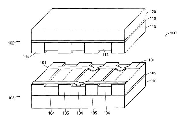
Figure 1 illustrates an exemplary electromechanical memory array 100 in
exploded view. In this embodiment, the array contains a layer of nanotube
ribbons
101 between an upper structure 102 and a lower structure 103.
The lower structure 103 includes a plurality of generally parallel
electrically
conductive traces 104, disposed between generally parallel and upwardly-
protruding
supports 105. The traces 104 and supports 105 are generally perpendicular to
the
ribbons 101. The traces and supports are arranged over a gate oxide layer 109
and
silicon substrate 110.
The upper structure 102 is similar to the lower structure. The upper structure
102 includes a plurality of generally parallel electrically conductive traces
114,
6
CA 02471380 2004-06-22
WO 03/058730 PCT/US02/41026
disposed between generally parallel and downwardly-protruding supports 115.
The
traces 114 and supports 11 S are generally perpendicular to the ribbons 101.
The
traces and supports are arranged over a gate oxide layer 119 and silicon
substrate 120.
For both the upper and lower structures 102, 103, the electromechanically
responsive elements 101 are nanotube ribbons. However, other materials,
including
nanotubes, may be used. Under certain preferred embodiments, a nanotube ribbon
101 has a width of about 180 nm and is pinned to insulating supports 102 (more
below). For both the upper and lower structures 102, 103, the traces
104, 114 may be made of any suitable electrically conductive material and may
be
arranged in any of a variety of suitable geometries. Certain preferred
embodiments
utilize n-doped silicon to form such traces, preferably no wider than the
nanotube belt
101, e.g., about 180 nm.
For both the upper and lower structures 102, 103, the supports 102 and 112,
likewise, may be made of a variety of materials and geometries, but certain
preferred
embodiments utilize insulating material, such as spin-on-glass (SOG). The
preferred
thickness (height) must equal or exceed the height of the electrodes
preferably from
100nm to 1 micron.
As will be explained below, under certain embodiments, the ribbons 101 are
held between the contacting supports by friction. In other embodiments, the
ribbon
may be held by other means, such as by anchoring the ribbons to the supports
using
any of a variety of techniques. The nanotube ribbons 101 are also pinned to
the upper
surfaces of lower supports 102 by the upper supports being deposited on top of
the
lower supports. Evaporated or spin-coated material such as metals,
semiconductors or
insulators--especially silicon, titanium, silicon oxide or polyimide-may be
used to
increase the pinning strength. The friction interaction can be increased
through the
use of chemical interactions, including covalent bonding through the use of
carbon
compounds such as pyrenes or other chemically reactive species. See R.J. Chen
et al.,
"Noncovalent Sidewall Functionalization of Single-Walled Carbon Nanotubes for
Protein Immobilization," J. Am. Chem. Soc., vol. 123, pp. 3838-39 (2001), and
Dai et
al., Appl. Phys. Lett., vol. 77, pp. 3015-17 (2000), for exemplary techniques
for
pinning and coating nanotubes by metals. See also WO 01/03208 for techniques.
Each instance where a ribbon crosses corresponding, oppositely-disposed
traces defines a memory or logic cell. The actual number of such cells is
immaterial
7
CA 02471380 2004-06-22
WO 03/058730 PCT/US02/41026
to understanding the invention, but the technology may support devices having
information storage capacities at least on the order of modern nonvolatile
circuit
devices.
Figures 2-4 are cross-sectional diagrams of a cell and illustrate various
states
of the device. For example, a given cell may be used to have three states
assigned as
"on" and "ofp' states. State 106 may be assigned as an "off," and states 107
and 108
may be assigned as "on" states 107 and 108.
When the device is in state 106, the ribbon 101 is separated from both
electrically conductive traces 104 and 114 by a distance 110. (The figure may
suggest
that the distances 110 between the ribbon and a corresponding trace is equal,
but they
need not be.) This state may be electrically detected in any of a variety of
ways
described in the foregoing references incorporated by reference. When the cell
is in
state 107, shown in figure 3, the ribbon is deflected toward trace 104. When
the cell is
in state 108, shown in figure 4, the ribbon is deflected toward trace 114. In
this
arrangement, an "off' state corresponds to the ribbon-trace junction being an
open
circuit, which may be sensed as such on either the ribbon 101 or trace 104
when
addressed. In the "on" states, the ribbon-trace junction is an electrically
conducting,
rectifying junction (e.g., Schottky or PN), which may be sensed as such on
either the
ribbon 101 or trace 104 when addressed.
Under certain embodiments in which the lateral spacing between the supports
102 is about 180 nm, the relative separation 110 from the top of an insulating
support
102 to the deflected position where the belt 101 attaches to electrode 104 or
114
should be approximately 5-50 nm. The magnitude of the separation 110 is
designed
to be compatible with electromechanical switching capabilities of the memory
device.
The 5-50 nm separation is preferred for certain embodiments utilizing ribbons
101
made from carbon nanotubes, and reflects the specific interplay between strain
energy
and adhesion energy for the deflected nanotubes. Other separations may be
preferable
for other materials.
Switching between these states is accomplished by the application of specific
voltages across the nanotube belt or wire 101 and one or more of its
associated
conductive traces 104,114. Switching forces are based on the interplay of
electrostatic
attraction and repulsion between the nanotube ribbon and the electrodes.
In certain embodiments, there is a high ratio between resistances in the "off
8
CA 02471380 2004-06-22
WO 03/058730 PCT/US02/41026
and the two "on" states. The differences between resistances in the "ofd' and
"on"
states provides a means to read which state a junction is in. In one approach,
a
"readout current" is applied to the nanotube belt or electrode and the voltage
across
the junction is determined with a "sense amplifier" on the traces. Reads are
non-
destructive, meaning that the cell retains its state, and no write-back
operations are
needed as is required with semiconductor DRAMS.
As alluded to above, the three-trace junctions of preferred embodiments bring
their own advantages. By allowing for use of tristable memory cells, more
information may be stored or represented by a given cell. Moreover, even if
only one
of the "on" states were used, three-trace junctions may increase switching
speeds
from the ability to use both conductive traces in concert to apply forces to
move an
electromechanically responsive trace 101. Furthermore, advantages in increased
reliability and defect tolerance can come from the redundancy permitted, by
the
presence of two conductive traces in each cell. Each of the two conductive
traces may
be separately used to apply forces to move an electromechanically responsive
trace,
and each of the two conductive traces may serve as the "contact" for one of
two
alternative "on" states. Thus, the failure of one conductive trace may not be
fatal to
junction performance. In addition, by disposing the ribbons 101 between upper
and
lower structures 102, 103, the ribbons are effectively sealed and protected.
Among
other things this facilitates packaging and distribution, and it allows the
nanotube-
technology arrays to be more easily incorporated into other circuit and
systems such
as hybrid circuits. The lateral nature of the electrical architecture can also
facilitate
the production of stackable memory layers and the simplification of various
interconnects.
Figure 5 illustrates a method of making certain embodiments of NTRCM
devices 100. A first intermediate structure 500 is created or provided as
explained in
the incorporated patent applications, cited above. The structure 500 includes
a silicon
substrate 502 having a gate dielectric layer 504 (such as silicon dioxide) and
an
insulating support layer 506 (such as spin-on-glass (SOG)) that contains a
plurality of
supports 508. In this instance, the supports 508 are formed by rows of
patterned
insulating material, though many other arrangements are possible, such as a
plurality
of columns.
Conductive traces 510 extend between supports 508. These conductive
9
CA 02471380 2004-06-22
WO 03/058730 PCT/US02/41026
electrodes can be fabricated from a single material such as n-doped silicon or
from a
combination of material layers including metal and silicon layers. Acceptable
materials for the conductive electrodes include copper, titanium, tungsten,
and
platinum, or other metals or semiconductors, such as silicon, compatible with
standard
fabrication lines. In this instance, the traces 510 are shown as essentially
contacting
the supports 508, but other arrangements are possible, as are other
geometries, such as
ones characterized by non-rectangular transverse cross-sections (e.g.,
triangular or
trapezoidal).
Sacrificial layers 518 are disposed above the conductive traces 510 so as to
define one planar surface 520 with the upper surface of the supports 508. This
planar
surface, as has been explained previously in the incorporated applications,
facilitates
growth of a non-woven fabric of single-walled carbon nanotubes (SWNTs) which
is
primarily one nanotube thick.
Under certain embodiments, a nanotube film is first grown on surface 520 and
then patterned, e.g., by photolithography and etching, to define a layer of
ribbons 522
(see also 101 in figure 1). The ribbons of non-woven nanotube fabric lie on
the planar
surface 520 and cross (for example, perpendicularly) the underlying traces
510. The
resulting intermediate structure 524 is the lower structure 102 referred to
above, with
the exception that structure 524 includes the sacrificial layer 518.
The lower intermediate structure 524 may be formed in many ways. Several
such ways are described in the incorporated patent applications, cited above.
In
addition, various ways are implicitly suggested through the description below
of
different ways of constructing analogous structures sitting on top of the
lower array.
An upper intermediate structure 526 may be formed separately, and it may be
placed on top of the patterned carbon nanotube film layer 522 to yield
intermediate
structure 540. Like the lower intermediate structure 524, the upper
intermediate
structure 526 includes an insulating support layer 528 (e.g., SOG) that
contains a
plurality of supports 530. In the pictured embodiment, the supports 530
consist of
rows of patterned insulating material, but, as with the lower structure, many
arrangements are possible, such as ones containing a plurality of columns.
Moreover,
the insulating supports may be made from a variety of materials.
Conductive traces 532, separated from the nanotubes by a second set of
sacrificial layers 534, extend between supports 530. The conductive traces 532
are
CA 02471380 2004-06-22
WO 03/058730 PCT/US02/41026
shown as essentially contacting the supports 530, but other arrangements and
geometries are possible, as described for the conductive traces 510 in
intermediate
500. A gate dielectric layer 536 and a conductive ground layer 538 are
deposited on
top of the supports 530 and traces 532.
To generate the target structure 542 featuring suspended, tristable nanotube
junctions 544, the lower and upper sacrificial layers 518 and 534,
respectively, have
to be removed from intermediate structure 540, as by using wet or dry chemical
etchants including acids or bases.
Before describing methods for producing the upper array 526 in greater detail,
a few aspects regarding the fabrication process and its product are worth
pointing out.
The first is that the various growth, patterning, and etching operations may
be
performed using conventional techniques, such as lithographic patterning.
Currently,
these techniques can lead to feature sizes (e.g., the width of ribbon 101) of
about 180
nm to as low as 130 nm, but the physical characteristics of the components are
amenable to even smaller feature sizes that may be accessible to future
manufacturing
processes.
A second point is that, because the nanotube ribbons are in place before
construction of the upper array begins, there is some more flexibility in the
choice of
materials for the upper array. In particular, while the choice of materials
for the lower
electrodes is limited to those substances that will survive the high
temperature of the
nanotube growth process, the choice of materials for the upper electrodes is
not so
constrained.
The final point is that interconnect fabrication can be applied using standard
metallization and CMOS logic or using nanoelectromechanical addressing as
previously explained in the incorporated patent applications, cited above.
Such
addressing can also be done utilizing a tristable nanoelectromechanical
addressing
logic scheme.
Three possible methods for generating the upper intermediate structure 526 are
described in connection with figures 6A-B, Figures 7A-B, and Figures 8A-B.
Figures 6A-B show one approach for producing a three-trace structure 542. A
lower intermediate structure 524 is provided or constructed using the
techniques
identified above. A sacrificial layer 602 (about 10-20 nm high) and an n-doped
silicon layer 604 are then added using a CVD process, sputtering,
electroplating, or a
11
CA 02471380 2004-06-22
WO 03/058730 PCT/US02/41026
different deposition process.
To generate the conductive traces 610, a photoresist layer may be spin-coated
on layer 604 and subsequently exposed and developed to create cavities which
lie
directly over the underlying supports 508.
Reactive ion etching (RIE) or the like may then be used to etch the electrode
and sacrificial layers 604 and 602 to form cavities 608 and to define upper-
layer
electrodes 610 that are positioned directly above the underlying electrodes
510. As
shown in figure 6B, the cavities 608 are then filled and covered with a planar
layer
609 of insulating material such as spin-on-glass (SOG) or polyimide. The
insulating
layer 609 is backetched with RIE or a plasma to the same height as the
electrodes 610
so as to form a planar surface 616. A gate dielectric layer 620 is provided
above the
surface 616 to separate the electrodes 610 from the upper electrical ground
layer 622.
This layer 622 serves the additional purpose of providing a hermetic seal
covering the
entire memory structure.
The resulting intermediate structure 540 is then processed so that the lower
and upper sacrificial layers 518 and 534, respectively, are removed to result
in
structure 542, as discussed above in connection with figure 5.
Figures 7A-B show another approach for producing a three trace structure 542.
A lower intermediate structure 524 like that described in connection with
Figure 5 is
provided or constructed. A sacrificial layer 702 (about 10-20 nm high) can be
selectively grown directly above the underlying sacrificial layer 518, e.g.,
by using a
selective CVD process involving self complementary materials such as titanium,
to
produce intermediate structure 700. The resulting cavities 704 are filled and
covered
with a planar layer 708 of an insulating material such as spin-on-glass (SOG)
or
polyimide. The insulating layer 708 is backetched with RIE or a plasma to a
height
710 equal to the intended total height of the upper sacrificial layer 702 and
the upper
conductive electrodes 724. A photoresist layer may be spin-coated on layer 708
and
subsequently exposed and lithographically developed to create cavities which
lie
directly over the underlying electrodes S 10.
As illustrated by Figure 7B, reactive ion etching (RIE) or the like may then
be
used to etch the upper support layer 708 to form cavities 714 and to define
the upper
supports 716. The cavities 714 are filled and covered with a planar layer
consisting of
n-doped silicon or other suitable electrode-forming materials, and this layer
is
12
CA 02471380 2004-06-22
WO 03/058730 PCT/US02/41026
backetched with RIE or a plasma to the same height 710 as the remaining
portions of
the support layer 722, the result being intermediate 718. The top surfaces of
the upper
electrodes 724 and the supports 722 form a planar surface 726. A gate
dielectric layer
730 is deposited on top of intermediate structure 718 to separate the upper
electrodes
724 from the upper electrical ground conductive layer 732 (e.g., silicon),
which is
added on top of the gate dielectric layer. This results in structure 540 like
those
described above. Layer 732 serves the additional purpose of providing a
hermetic
seal covering the entire memory structure.
The resulting intermediate structure 540 is then processed so that the lower
and upper sacrificial layers 518 and 534, respectively, are removed to result
in
structure 542, as discussed above in connection with figure 5.
Figures 8A-B show another approach for producing a three trace structure 542.
Intermediate structure 700 (as explained above) is provided or created. Under
this
approach, though, the cavities 704 are filled with n-doped silicon or other
suitable
electrode-forming materials to form a planar layer 804. The electrode layer
804 is
backetched with RIE or a plasma to approximately the same height 710 as
previously
described. A photoresist layer may be spin-coated on layer 804 and
subsequently
exposed and lithographically developed to begin the creation of cavities 808
which lie
directly over the underlying supports 508.
As illustrated in Figure 8B, reactive ion etching (RIE) or the like may then
be
used to complete the cavities 808 and to define the upper electrodes. The
cavities 808
of intermediate 806 are then filled and covered with a planar insulating
layer,
consisting, for example, of SOG or polyimide. The insulating layer is
backetched
with RIE or a plasma to form the supports 722 with a height 710 equal to the
total
height of the upper sacrificial layer 702 and the upper silicon electrodes
724. The
result is intermediate structure 718, with a flat surface 726 as previously
described.
Substrate 718 is converted into substrate 728 by adding gate dielectric and
upper
electrical ground layers as described above.
The resulting intermediate structure 540 is then processed so that the lower
and upper sacrificial layers 518 and 534, respectively, are removed to result
in
structure 542, as discussed above in connection with figure 5.
Under other embodiments of the invention, from those described above, the
upper electrodes are not located directly over the lower electrodes but,
instead, are
13
CA 02471380 2004-06-22
WO 03/058730 PCT/US02/41026
shifted (e.g., displaced by half their width) relative to the lower
electrodes. This
approach, among other things, facilitates the use of certain techniques for
removing
sacrificial layers.
Figure 9 illustrates a method of making these "shifted" embodiments of
NTRCM devices. A first intermediate structure 500, as described above, is
created or
provided. Structure 500 is then converted, as described above, to intermediate
524
featuring patterned nanotube ribbons 522 on top of intermediate 500. Upper
insulating
supports 902 are deposited onto the lower supports 508, and upper sacrificial
layers
904 having the same height as the upper supports 902 are deposited on top of
ribbons
522 but in alignment with the lower sacrificial layers 518, so as to create a
flat surface
906. The height of the upper sacrificial layers 904 and upper supports 902 is
approximately the same as the height of the lower sacrificial layer 518, e.g.,
10-20 nm
on average. The upper supports 902 and upper sacrificial layers 904 may be
made of
the same materials as the corresponding lower layers but are not limited to
these
materials.
Conductive traces 908 of n-type silicon electrodes, or some other suitable
material or material combination, are provided on top of the flat surface 906
so that
they run parallel to the lower conductive traces 510 and so that at least a
portion of the
traces 908 (but not their entirety) are aligned with the traces 510. The
completed
upper array 910 of the resulting intermediate 900 includes upper supports 902,
upper
sacrificial layers 904, and upper electrodes 908. The upper conductive traces
908 in
intermediate 900 are not directly located above the lower electrode traces
510, but are
shifted by a certain amount (e.g., by half their width) relative to the lower
traces 510.
To generate the freely suspended tristable nanotube junctions 914 of the
target
structure 912, the lower sacrificial layer 518 and upper sacrificial layer 904
are
removed using wet or dry chemical etchants including acids or bases.
The upper traces 908 are shown as having rectangular cross-sections and
widths similar to those of the lower supports 508 and lower electrodes 510,
but
neither the shapes nor the widths of the upper traces 908 is limited to these
parameters. Narrower or wider traces of different cross-sections, e.g.,
trapezoidal or
triangular, can be envisioned. Furthermore, while the choice of material for
the lower
array 524 is somewhat limited so that the materials are compatible with the
growth
conditions for the carbon nanotubes or nanotube fabrics (e.g., relatively high
14
CA 02471380 2004-06-22
WO 03/058730 PCT/US02/41026
temperature), the upper array 910 is fabricated after nanotube growth so that
a wider
variety of materials can be used for the upper supports 902, upper sacrificial
layers
904, and upper electrodes 908. For example, materials that are only stable up
to
relatively low temperatures, such as polyimides, other polymers or low melting
point
metals (e.g. aluminum), can be used for the upper array 910.
Figures 10-12 are cross-sectional diagrams of a cell having a shifted upper
electrode and illustrate various states of the device. Analogously to the
above
embodiments the states may be assigned with some meaning, such as "on" and
"ofp'
states, or assigned to non-binary encoding. For example, figure 10 shows a
junction
that may be assigned as an "ofp' state, whereas figures 11 and 12 show
junctions in
different "on" states. The description of these states is analogous to that of
figures 2-4
and thus will not be repeated. Like reference numerals to those of figures 2-4
have
been used to show corresponding features of these embodiments and states.
Figures 13A-B show one approach for producing a three-trace structure 912.
A lower intermediate structure 524 is provided or constructed using the
techniques
identified above. A support layer 1302 of about the same height as the lower
sacrificial layer 518 is deposited to generate intermediate structure 1300.
The layer
1302 is then patterned by photolithography and etching techniques, such as
RIE, to
create the supports 902 and to define cavities 1306 of intermediate structure
1304.
The cavities 1306 are filled with a planar sacrificial layer which is then
backetched by RIE or some other etching technique until the sacrificial layer
904 has
the same height as the upper supports 902 and a planar surface 906 is formed.
The
intermediate structure 1310 so formed then has a layer of electrode material,
such as
n-type silicon, deposited on top of surface 906, which is then patterned by
photolithography and etching techniques, such as RIE, to define conductive
electrode
traces 908 and to form intermediate structure 900.
The upper and lower sacrificial layers 904 and 518 are then removed, as
explained in conjunction with Figure 9, to generate the freely suspended,
tristable
nanotube junctions 914 of the target structure 912.
Figures 14A-B show another approach for producing a three-trace structure
912. Intermediate structure 524 is provided or created and then transformed
into
intermediate 1400 by evaporation onto its surface of an upper sacrificial
layer 1402 of
about the same height as the lower sacrificial layer 518. This sacrificial
layer is then
CA 02471380 2004-06-22
WO 03/058730 PCT/US02/41026
patterned by lithography and etching to form sacrificial layer lines 1406
separated by
cavities 1408 of intermediate 1404.
The cavities 1408 are then filled by a flat layer of support material which is
backetched to the same height as the sacrificial layer lines 904 to form a
flat surface
906 and to form intermediate structure 1310. Intermediate 1310 is converted
into
intermediate 900 as explained in conjunction with Figure 13B. The upper and
lower
sacrificial layers 904 and 518 are removed to form the target structure 912
containing
freely suspended, tristable nanotube junctions 914.
Figure 15 shows another approach for producing a three-trace structure 912.
First, support layers 902 (about 10-20 nm high) are selectively grown on top
of the
lower structure 524 directly above the lower supports 508, e.g., by using a
selective
CVD process involving self-complementary materials such as titanium or silicon
dioxide. The resulting intermediate 1304 is then converted successively into
intermediate 1310, intermediate 900, and finally the target structure 912, as
described
above in conjunction with Figure 13B.
Figure 16 shows another approach for producing a three-trace structure 912.
Sacrificial layers 904 are selectively deposited on the lower array 524 to
form
intermediate 1404. Intermediate 1404 is then converted via intermediates 1310
and
900 into the target structure 912, as described above in conjunction with
Figure 14B.
Figure 17 shows another approach for producing a three-trace structure 912.
Intermediate 524 is created or provided. A sacrificial layer 1402, made of the
same
material as the lower sacrificial layer 518, and an electrode layer 1702 are
deposited
to form structure 1700. The electrode layer 1702 is then patterned by
lithography and
RIE to form electrode lines 908. Subsequently, the exposed part of the upper
and
lower sacrificial layers are removed by R1E to form intermediate 1706. The
remaining sacrificial material 1708 is located only underneath the electrode
lines 908.
Where sacrificial material was removed, the now freely suspended nanotube
ribbons
form junctions 1710 with a freely suspended length, in the embodiment pictured
(in
which array elements are assumed to have been made as small as possible), of
approximately half the resolution limit of the lithography used for
patterning.
To form freely suspended, tristable junctions, the part 1712 of the
sacrificial
material remaining directly above the lower electrodes 510 is removed. This
can be
accomplished by utilizing the faster differential solubility of this
sacrificial material
16
CA 02471380 2004-06-22
WO 03/058730 PCT/US02/41026
1712 compared to the sacrificial material 1714 remaining directly above the
lower
insulating supports 508. The sacrificial material 1712 directly above the
lower
electrodes dissolves faster because it is more accessible to the etchant than
the part
1714 of the remaining sacrificial layer directly above the lower supports 508.
As a
result, by applying etchant and then stopping the etching process at the
appropriate
time, the target structure 1716, featuring freely suspended, tristable
nanotube junctions
914 can be fabricated.
Figures 18A-B illustrate yet another approach for producing a three-trace
structure 912. Intermediate 1800 is produced by evaporating a sacrificial
layer 1802
and an electrode material layer 1702 onto intermediate 524. The upper
sacrificial
layers 1802 are made of a material that has different etching characteristics
than the
lower sacrificial layers 518.
The electrode material layer 1702 is patterned to form the electrode lines 908
of intermediate 1804. Subsequently, the exposed region of the sacrificial
layer 1802
in between electrodes 908 is removed by RIE to form intermediate 1806 of
Figure
18B. Then the lower sacrificial layer 518 is removed by etching to form
intermediate
1808. The remaining portions 1810 of the upper sacrificial layers directly
above the
lower electrodes 510 are removed by utilizing their higher differential
solubility
compared to the portions 1812 of sacrificial material directly above the lower
supports
508. Because sacrificial material 1810 directly above the lower electrodes is
much
more easily accessed than sacrificial material 1812 directly above the lower
supports,
the material directly above the lower electrodes etches faster. Thus, by
applying
etchant but stopping the etching process at the appropriate time, the freely
suspended,
tristable junctions 914 of the target structure 1814 can be generated.
Additional Embodiments
In general, it should be noted that the feature sizes described above are
suggested in view of modern manufacturing techniques. Other embodiments may be
made with much smaller (or larger) sizes that reflect manufacturing
capabilities.
The target structures and processes described above do not exhaust the range
of embodiments of the present invention. Subsequent metallization may be used
to
add addressing electrodes to an array of tristable junctions such as that
pictured in
Figure 1. Other embodiments could use nanotube technology, whether in
individual
17
CA 02471380 2004-06-22
WO 03/058730 PCT/US02/41026
wire or belt form, to implement addressing of memory cells instead of using
metallized electrodes and CMOS addressing logic (not shown). Such potential
use of
nanotube technology to select memory cells for reading or writing operations
would
further integrate nanotubes into system design and might add beneficial
functionality
to higher-level system design. For example, under this approach of using
nanotube
technology for both memory and addressing, the memory architecture could
inherently store the last memory address as well as memory contents in a
nonvolatile
manner.
Another set of embodiments would use different materials in place of the
nanotube ribbons described above. Of course, individual nanotubes could be
used
instead of ribbons, albeit with the disadvantages relative to ribbons
discussed above.
In addition, other materials with electronic and mechanical properties
suitable for
electromechanical switching could be envisioned. These materials would have
properties similar to carbon nanotubes but with different and likely reduced
tensile
strength. For a material to qualify, its tensile strain and adhesion energies
would need
to fall within a range that allowed for bistability or tristability, and that
ensured that
required electromechanical switching properties exist within acceptable
tolerances.
Other embodiments could feature additional electrodes consisting of n-doped
silicon on top of some metal or semiconductor conductive traces. The
additional
electrodes would provide rectifying junctions in the ON state so that no
multiple
current pathways exist.
Embodiments could also feature any of various other widely accepted and
used methods to prevent the occurrence of electrical crosstalk (i.e., multiple
current
pathways) in crossbar arrays. Tunnel barriers could be added on top of the
static,
lithographically fabricated electrodes to prevent the formation of ohmic ON
states. In
such embodiments, no leakage currents would occur at zero bias voltage, and a
small
bias voltage would have to be applied for any significant number of charge
carriers to
overcome the barrier and tunnel between crossing traces.
Additional embodiments could make use of methods to increase adhesion
energies through the use of ionic, covalent or other forces to alter the
interactions
between the electromechanical switching elements and the electrode surfaces.
Such
methods can be used to extend the range of bistability and tristability within
the
junctions.
18
CA 02471380 2004-06-22
WO 03/058730 PCT/US02/41026
Further embodiments could be produced by functionalizing nanotubes with
planar conjugated hydrocarbons such as pyrenes. These hydrocarbons could
enhance
the internal adhesion between nanotubes within the ribbons.
Moreover, many of the above benefits may be achieved by embodiments that
do not utilize the "sandwich-type" of architecture of having the
electromechanically-
responsive element disposed between two electrodes. For example, two generally
parallel traces disposed on one side of the electromechanically-responsive
element
may improve fault tolerance and the like.
In addition, certain embodiments used a shifted upper trace to define an
opening to the sacrificial layers to facilitate the removal of the sacrificial
layers.
Other approaches may be used to define such openings, for example, by shaping
the
upper trace appropriately to define such an opening.
It will be further appreciated that the scope of the present invention is not
limited to the above-described embodiments, but rather is defined by the
appended
claims, and that these claims will encompass modifications of and improvements
to
what has been described.
What is claimed is:
19