Note: Descriptions are shown in the official language in which they were submitted.
CA 02471536 2004-06-23
WO 03/058376 PCT/US02/38755
METHOD AND APPARATUS FOR
REGENERATING A CLOCK FOR AUXILIARY
DATA TRANSMITTED OVER A SERIAL LINK
WITH VIDEO DATA
CROSS-REFERENCE TO RELATED APPLICATION
This application is a continuation-in-part of pending U.S. Patent Application
No. 101036,234, filed on December 24, 2001, and assigned to the assignee of
the
present application, and a continuation-in-part of pending U.S. Patent
Application No.
10/095,422, filed on March 12, 2002, and assigned to the assignee of the
present
application,
TECHI~IICAL FIELD OF THE INVENTION
The invention pertains to methods and systems for transmitting encoded video
data and at least one other stream of encoded data (e.g., encoded video data
and packets
of encoded audio and/or other auxiliary data) over a serial link, and to
transmitters and
receivers for use in such systems. In preferred embodiments, the serial link
is a
transition minimized differential signaling ("TMDS") link, or a link having
some but
not all of the characteristics of a TMDS link.
BACKGROUND OF THE INVENTION
Throughout the specification, decimal ("base 10") numbers are represented
using no additional prefixes or suffixes, and the following notation is
sometimes used:
"bit 0" denotes the least-significant bit of a byte or word;
the prefix "Ox" denotes that the following symbol is a hexadecimal
representation of a number (for example "OxC" denotes a binary number 1100);
and
the prefix "Ob" denotes that the following symbol is a binary (base-2)
representation of a number (for example "Ob1000" denotes a decimal number ~).
Elements of this invention are based upon properties of a serial link. Various
serial links for transmitting data and clock signals are well known.
One conventional serial link, used primarily for high-speed transmission of
video data from a host processor (e.g., a personal computer) to a monitor, is
known as a
-1-
CA 02471536 2004-06-23
WO 03/058376 PCT/US02/38755
transition minimized differential signaling interface ("TMDS" link). The
characteristics of a TMDS Iink include the following:
1. video data are encoded and then transmitted as encoded words (each 8-bit
word of digital video data is converted to an encoded 10-bit word before
transmission);
a. the encoding determines a set of "in-band" words and a set of "out-
of band" words (the encoder can generate only "in-band" words in response to
video data, although it can generate "out-of band" words in response to
contxol
or sync signals. Each in-band word is an encoded word resulting from encoding
of one input video data word. All words transmitted over the link that are not
in-
band words are "out-of band" words);
b. the encoding of video data is performed such that the in-band words
are transition minimized (a sequence of in-band words has a reduced or
minimized number of transitions);
c. the encoding of video data is performed such that the in-band words
are DC balanced (the encoding prevents each transmitted voltage waveform that
is employed to transmit a sequence of in-band words from deviating by more
than a predetermined threshold value from a reference potential. Specifically,
the tenth bit of each "in-band" word indicates whether eight of the other nine
bits thereof have been inverted during the encoding process to correct for an
imbalance between running counts of ones and zeroes in the stream of
previously encoded data bits);
2. the encoded video data and a video clock signal are transmitted as
differential
signals (the video clock and encoded video data are transmitted as
differential signals
over conductor pairs);
3. three conductor pairs are employed to transmit the encoded video, and a
fourth conductor pair is employed to transmit the video clock signal; and
4. signal transmission occurs in one direction, from a transmitter (typically
associated with a desktop or portable computer, or other host) to a receiver
(typically an
element of a monitor or other display device).
A use of the TMDS serial link is the "Digital Visual Interface" interface
("DVI"
link) adopted by the Digital Display Working Group. It will be described with
reference
-2-
CA 02471536 2004-06-23
WO 03/058376 PCT/US02/38755
to Fig. 1. A DVI link can be implemented to include two TMDS links (which
share a
common conductor pair for transmitting a video clock signal) or one TMDS Link,
as
well as additional control lines between the transmitter and receiver. The DVI
link of
Fig. 1 includes transmitter 1, receiver 3, and the following conductors
between the
transmitter and receiver: four conductor pairs (Channel 0, Channel 1, and
Channel 2 for
video data, and Channel C for a video clock signal), Display Data Channel
("DDC")
Iines for bidirectional communication between the transmitter and a monitor
associated
with the receiver in accordance with the conventional Display Data Channel
standard
(the Video Electronics Standard Association's "Display Data Channel Standard,"
Version 2, Rev. 0, dated April 9, 1996), a Hot Plug Detect (I-~D) line (on
which the
monitor transmits a signal that enables a processor associated with the
transmitter to
identify the monitor's presence), Analog lines (for transmitting analog video
to the
receiver), and Power lines (for providing DC power to the receiver and a
monitor
associated with the receiver). The Display Data Channel standard specifies a
protocol
for bidirectional communication between a transmitter and a monitor associated
with a
receiver, including transmission by the monitor of an Extended Display
Identification
("EDID") message that specif es various characteristics of the monitor, and
transmission by the transmitter of control signals for the monitor.
Transmitter 1
includes three identical encoder/serializer units (units 2, 4, and 6) and
additional
circuitry (not shown). Receiver 3 includes three identical recovery/decoder
units (units
~, 10, and 12) and inter-channel alignment circuitry 14 connected as shown,
and
additional circuitry (not shown).
As shown in Fig. l, circuit 2 encodes the data to be transmitted over Channel
0,
and serializes the encoded bits. Similarly, circuit 4 encodes the data to be
transmitted
over Channel 1 (and serializes the encoded bits), and circuit 6 encodes the
data to be
transmitted over Channel 2 (and serializes the encoded bits). Each of circuits
2, 4, and
6 responds to a control signal (an active high binary control signal referred
to as a "data
enable" or "DE" signal) by selectively encoding either digital video words (in
response
to DE having a high value) or a control or synchronization signal pair (in
response to
DE having a low value). Each of encoders 2, 4, and 6 receives a different pair
of
control or synchronization signals: encoder 2 receives horizontal and vertical
-3-
CA 02471536 2004-06-23
WO 03/058376 PCT/US02/38755
synchronization signals (HSYNC and VSYNC); encoder 4 receives control bits
CTLO
and CTLl; and encoder 6 receives control bits CTL2 and CTL3. Thus, each of
encoders 2, 4, and 6 generates in-band words indicative of video data (in
response to
DE having a high value), encoder 2 generates out-of band words indicative of
the
values of HSYNC and VSYNC (in response to DE having a low value), encoder 4
generates out-of band words indicative of the values of CTLO and CTLl (in
response to
DE having a low value), and encoder 6 generates out-of band words indicative
of the
values of CTL2 and CTL3 (in response to DE having a low value). In response to
DE
having a low value, each of encoders 4 and 6 generates one of four specific
out-of band
words indicative of the values 00, O1, 10, or 11, respectively, of control
bits CTLO and
CTLl (or CTL2 and CTL3).
It has been proposed to encrypt video data transmitted over a serial link. For
example, it has been proposed to use a cryptographic protocol known as "High-
bandwidth Digital Content Protection" ("HDCP") to encrypt digital video to be
transmitted over a DVI link and to decrypt the data at the DVI receiver. A DVI
transmitter implementing HDCP outputs a 24-bit bus, known as coot[23:0],
during the
video active period (i.e. when DE is high). This 24-bit tout data is
"Exclusive Ored" (in
logic circuitry in the transmitter) with the 24-bit RGB video data input to
the
transmitter in order to encrypt the video data. The encrypted data is then
encoded
(according to the TMDS standard) for transmission. The same tout data is also
generated in the receiver. After the encoded and encrypted data received at
the receiver
undergoes T1VIDS decoding, the tout data is processed together with the
decoded video
in logic circuitry in order to decrypt the decoded data and recover the
original input
video data.
Before the transmitter begins to transmit HDCP encrypted, encoded video data,
the transmitter and receiver communicate bidirectionally with each other to
execute an
authentication protocol (to verify that the receiver is authorized to receive
protected
content, and to establish shared secret values for use in encryption of input
data and
decryption of transmitted encrypted data). After the receiver has been
authenticated,
the transmitter calculates the initial set of encryption keys (for encrypting
the first line
of input video data) in response to a control signal and sends the control
signal to the
-4-
CA 02471536 2004-06-23
WO 03/058376 PCT/US02/38755
receiver (during each vertical blanking period, when DE is low) to cause the
receiver to
calculate an initial set of decryption keys (for decrypting the first received
and decoded
line of transmitted video data). Following generation of the initial set of
encryption/decryption keys, each of the transmitter and receiver performs a re-
keying
operation during each blanking (vertical or horizontal) interval to generate a
new set of
keys for encrypting (or decrypting) the next line of video data, and actual
encryption of
input video data (or decryption of received, decoded video data) is performed
using the
latest set of keys only when DE is high (not during the blanking intervals).
Each of the transmitter and receiver includes an HDCP cipher circuit
(sometimes referred to herein as an "HDCP cipher") including a linear feedback
shift
register (LFSR) module, a block module coupled to the output of the LFSR
module,
and an output module coupled to an output of the block module. The LFSR module
is
employed to re-key the block module in response to each assertion of an enable
signal,
using a session key (Ks) and frame key (Ki). The block module generates (and
provides to the LFSR module) the key Ks at the start of a session and
generates (and
applies to the LFMS module) a new value of key Ki at the start of each frame
of video
data (in response to a rising edge of a control signal which occurs in the
first vertical
blanking interval of a frame).
The block module comprises two halves, known as "Round Function K" and
"Round Function B." Round Function K includes 28-bit registers Kx, Ky, and Kz,
seven S-Boxes (each a 4. input bit by 4 output bit S-Box including a look-up
table), and
a linear transformation unit K. Round Function B includes 28-bit registers Bx,
By, and
Bz, seven S-Boxes (each a 4 input bit by 4 output bit S-Box including a look-
up table),
and a linear transformation unit B. Round Function K and Round Function B are
similar in design, but Round Function K performs one round of a block cipher
per
clock cycle to assert (to the output module) a different pair of 28-bit round
keys (Ky
and Kz) each clock cycle in response to the output of the LFSR module, and
Round
Function B performs one round of a block cipher per clock cycle, in response
to each
28-bit round key Ky from Round Function K and the output of the LFSR module,
to
assert (to the output module) a different pair of 28-bit round keys (By and
Bz) each
clock cycle. The transmitter generates value An at the start of the
authentication
-5-
CA 02471536 2004-06-23
WO 03/058376 PCT/US02/38755
protocol and the receiver responds to it during the authentication procedure.
The value
An is used to randomize the session key. The block module operates in response
to the
authentication value (Au) and an initialization value (Mi, also referred to as
an integrity
verification key) which is updated by the output module at the start of each
frame.
Each of linear transformation units K and B outputs 56 bits per clock cycle.
These output bits are the combined outputs of eight diffusion networks in each
transformation unit. Each diffusion network of linear transformation unit K
produces
seven output bits in response to seven of the current output bits of registers
Ky and Kz.
Each of four of the diffusion networks of linear transformation unit B
produces seven
output bits in response to seven of the current output bits of registers By,
Bz, and Ky,
and each of the four other diffusion networks of linear transformation unit B
produces
seven output bits in response to seven of the current output bits of registers
By and Bz.
The output module performs a compression operation on the 28-bit keys (By,
Bz, Ky and Kz) asserted to it (a total of 112 bits) by the block module during
each clock
I S cycle, to generate one 24-bit block of pseudo-random bits cout~23: OJ per
clock cycle.
Each of the 24 output bits of the output module consists of the exclusive OR
("XOR")
of nine terms.
In the transmitter, logic circuitry receives each 24-bit block of tout data
and
each input 24-bit RGB video data word, and performs a bitwise XOR operation
thereon
in order to encrypt the video data, thereby generating a word of encrypted RGB
video
data. Typically, the encrypted data subsequently undergoes TMDS encoding
before it
is transmitted to a receiver. In the receiver, logic circuitry receives each
24-bit block of
tout data and each recovered 24-bit RGB video data word (after the recovered
data has
undergone TMDS decoding), and performs a bitwise XOR operation thereon in
order to
decrypt the recovered video data.
Throughout the specification the expression "TMDS-like link" will be used to
denote a serial link capable of transmitting encoded data (e.g., encoded
digital video
data) and a clock for the encoded data, from a transmitter to a receiver, and
also capable
of transmitting (bidirectionally or unidirectionally) one or more additional
signals (e.g.,
encoded digital audio data or other encoded data) between the transmitter and
receiver,
that is or includes either a TlVmS link or a link having some but not all of
the
-6-
CA 02471536 2004-06-23
WO 03/058376 PCT/US02/38755
characteristics of a TMDS link. Examples of TMDS-like links include links that
differ
from TMDS links only by encoding data as N-bit code words (e.g., with N 10)
that
are not 10-bit TMDS code words, and links that differ from TMDS links only by
transmitting encoded video over more than three or less than three conductor
pairs.
There are several conventional TMDS-like links.
The term "transmitter" is used herein in a broad sense to denote any device
capable of encoding data and transmitting the encoded data over a serial link
(and
optionally also performing additional functions, which can include encrypting
the data
to be transmitted and other operations related to encoding, transmission, or
encryption
of the data). The term "receiver" is used herein in a broad sense to denote
any device
capable of receiving and decoding data that has been transmitted over a serial
link (and
optionally also performing additional functions, which can include decrypting
the
received data and other operations related to decoding, reception, or
decryption of the
received data). For example, the term transmitter can denote a transceiver
that
performs the functions of a receiver as well as the functions of a
transmitter. In a more
specific example, the term transmitter (with reference to a device that
transmits non-
audio auxiliary data over a TMDS-like link or other serial link) can denote a
transceiver
that is configured to receive video data and audio data over the link and to
transmit the
non-audio auxiliary data over the link.
Some TMDS-like links encode input video data (and other data) to be
transmitted into encoded words comprising more bits than the incoming data
using a
coding algorithm other than the specific algorithm used in a TMDS link, and
transmit
the encoded video data as in-band characters and the other encoded data as out-
of band
characters. The characters need not be classified as in-band or out-of band
characters
based according to whether they satisfy transition minimization and DC balance
criteria. Rather, other classification criteria could be used. An example of
an encoding
algorithm, other than that used in a TMDS link but which could be used in a
TMDS-
like link, is IBM 8b10b coding. The classification (between in-band and out-of
band
characters) need not be based on just a high or low number of transitions. For
example,
the number of transitions of each of the in-band and out-of band characters
could (in
CA 02471536 2004-06-23
WO 03/058376 PCT/US02/38755
some embodiments) be in a single range (e.g., a middle range defined by a
minimum
and a maximum number of transitions).
The data transmitted between the transmitter and receiver of a TMDS-like link
can, but need not, be transmitted differentially (over a pair of conductors).
Also,
although a TMDS link has four differential pairs (in the single pixel
version), three for
video data and the other for a video clock, a TMDS-like link could have a
different
number of conductors or conductor pairs.
Typically, the primary data transmitted by a TMDS link axe video data. What is
often significant about this is that the video data are not continuous, and
instead have
blanking intervals. These blanking intervals provide an opportunity (exploited
in some
embodiments of the present invention) for auxiliary data to be transported,
and they
represent unused bandwidth. However, many serial links do not transmit data
having
blanking intervals, and thus do not encode input data (for transmission) in
response to a
data enable signal. For example, audio serial links would typically transmit
continuous
data.
The expression "auxiliary data" is used in a broad sense herein to denote
digital
audio data or any other type of data other than video data and timing
information for
video data (e.g., a video clock). For example, timing information for audio
data (e.g., a
clock for recovering transmitted audio data) falls within the scope of
"auxiliary data."
Other examples of "auxiliary data" transmitted in accordance with the
invention
include computer keyboard signals, still image data (generated by a camera,
for
example), text data, control signals for a power supply, picture in picture
data, monitor
control information (audio volume, brightness, power state), control signals
for
indicator lights on a monitor or keyboard, non-audio or video control
information, etc.
The term "stream" of data, as used herein, denotes that all the data are of
the
same type and is transmitted with the same clock frequency. The term
"channel," as
used herein, refers to that portion of a serial link that is employed to
transmit data (e.g.,
a particular conductor or conductor pair between the transmitter and receiver
over
which the data are transmitted, and specific circuitry within the transmitter
and/or
receiver used for transmitting and/or recovery of the data) and to the
technique
employed to transmit the data over the link. Because it is desirable to
transmit many
_g_
CA 02471536 2004-06-23
WO 03/058376 PCT/US02/38755
different streams of auxiliary data in important applications of the
invention, preferred
embodiments of the invention provide multiple channels for transmission of
auxiliary
data, including channels for transmission of auxiliary data in both directions
over the
link (that is, with and against the direction of the video data). In some
implementations, a channel is employed to transmit one stream of auxiliary
data. In
other implementations, a channel is employed to transmit more than one stream
of
auxiliary data. In some embodiments of the invention, two (or more than two)
streams
of serial video data are transmitted (over one, two, or more than two
channels), and
either one, two, or more than two streams of serial auxiliary data are also
transmitted.
U.S. Patent 5,999,571, issued December 7, 1999, teaches (e.g., at col. 5)
that,
when the code words (indicative of video data) transmitted over a TMDS link
are
transition minimized words (a first subset of a set of code words),
synchronization
words (distinguishable from the transition minimized code words) can be
transmitted
over the link during "preamble" periods in which encoded video data are not
transmitted. The synchronization words can be transition maximized words that
are
members of a second subset (disjoint from the first subset) of the set of code
words.
U.S. 5,999,571 teaches that several (e.g., three) repetitions of a
synchronization word
should be transmitted consecutively, to allow the decoder (in the receiver)
rapidly and
accurately to identify a specific transition (e.g., the leading edge) of one
of the
synchronization words and thus to accomplish synchronization with the encoder
(in the
transmitter.
U.S. Patent 6,151,334, issued November 21, 2000, teaches transmission (over a
TMDS link) of several different types of encoded control words, each
distinguishable
from transition minimized code words indicative of data. At least some of the
control
words can be transition maximized words. One of the control words is a "data
stream
separation" word that is transmitted before or after a burst of data and is
indicative of
the start or end of a burst and the type of data transmitted during the burst.
Another one
of the control words is an "isochronous data transfer" word that is a
synchronization
character typically transmitted at the beginning or end of a blanking interval
and
indicates the type of the blanking interval (e.g., horizontal or vertical) and
distinguishes
between the beginning and the end of the blanking interval. For example, a
first
-9-
CA 02471536 2004-06-23
WO 03/058376 PCT/US02/38755
isochronous data transfer word indicates the start of a vertical blanking
interval, a first
data stream separation word then indicates the start of a burst of data in the
vertical
blanking interval, a second data stream separation word then indicates the end
of such
data burst, and a second isochronous data transfer word then indicates the end
of the
vertical blanking interval. Each of the first isochronous data transfer word,
the first data
stream separation word, the second data stream separation word, and the second
isochronous data transfer word is a transition maximized code word, a
transition
minimized code word can indicate each word of data of the data burst
(transmitted in
the vertical blanking interval), and the vertical blanking interval can be
followed by an
active video period comprising a third data stream separation word (indicative
of the
start of a stream of video data) followed by a stream of transition minimized
code
words indicative of the video data itself.
SUM1VIARY OF THE INVENTION
In a class of embodiments, the invention is a communication system including a
transmitter, a receiver, and a serial link (having at least one channel), for
transmitting a
stream of encoded video data and at least one other stream of encoded data
(e.g.,
encoded audio data) over each of one or more channels of the link from the
transmitter
to the receiver. In preferred embodiments, the serial link is a TMDS or TMDS-
like link.
In preferred embodiments, the transmitter sends encoded video to the receiver
over
each of one or more video channels of the link during active video periods,
and sends
packets including encoded auxiliary data (e.g., audio data) to the receiver
over each of
at least one of the video channels during data islands, wherein each of the
data islands
is a time interval that neither coincides with nor overlaps any of the active
video
periods. The transmitter preferably also transmits control data to the
receiver over each
of at least one of the video channels during control data periods, wherein the
control
data periods neither coincide with nor overlap any of the data islands and
neither
coincide with nor overlap any of the active video periods. Other aspects of
the
invention are transmitters for use in formatting and encoding multiple streams
of data
for transmission over a serial link, receivers for receiving and decoding
multiple
streams of encoded data transmitted over a serial link, and methods for
sending
-10-
CA 02471536 2004-06-23
WO 03/058376 PCT/US02/38755
multiple streams of encoded data over a serial link.
One or more packets can be transmitted in each data island. In each control
data
periods (sometimes referred to as a "control data interval" or "control
period"),
encoded control words (preferably including sync words and preamble words) can
be
transmitted.
In a class of systems that embody the invention, 8-bit video data words (each
encoded using the TlVmS encoding algorithm as a 10-bit, transition-minimized
code
word) are transmitted over the video channels of a TMDS link (or other TMDS-
like
link having multiple channels for transmitting serial video) during active
video periods.
During data islands between the active video periods, packets containing 4-bit
words
(typically including 4-bit audio data words), each encoded according to the
TMDS
encoding algorithm as a 10-bit, transition-minimized code word, and preferably
as a 10-
bit golden word, are transmitted over each of at least some of the video
channels.
During control data periods between the active video periods and data islands,
the
transmitter sends control words (each encoded as a 10-bit, transition-
maximized code
word indicative of two control bits: CTLO and CTLl, or CTL2 and CTL3) and sync
words (each encoded as a 10-bit, transition-maximized code word indicative of
two
sync bits: HSYNC and VSYNC) over the video channels. During each active video
period, HSYNC, VSYNC, CTLO, CTLl, CTL2, and CTL3 are assumed by the receiver
to maintain the values that they had when the active video period started.
Preferably, transition-minimized code words indicative of HSYNC and VSYNC
bits are sent (e.g., one code word per pixel clock cycle, each word indicative
of an
HSYNC bit, a VSYNC bit, a packet header bit, and another bits) over one
channel (e.g.,
CHO) during each data island.
In a class of embodiments, the invention is a system, including a receiver, a
transmitter; and a serial link comprising at least one video channel between
the
transmitter and the receiver. The transmitter is configured to receive video
data and
audio data, to generate encoded video data and encoded audio data by encoding
the
video data and audio data, to transmit code words indicative of the encoded
video data
over the video channel to the receiver in response to a pixel clock during
active video
periods, and to transmit packets including encoded auxiliary data to the
receiver during
-11-
CA 02471536 2004-06-23
WO 03/058376 PCT/US02/38755
data islands by transmitting code words indicative of the packets over the
link in
response to the pixel clock. The encoded auxiliary data include the encoded
audio data.
The transmitter is configured to include time code data in at least some of
the packets,
and the time code data together with the pixel clock are indicative of an
audio clock for
the audio data. In preferred embodiments in which the encoded video data are
transmitted over video channels of a TMDS link (during active video periods),
a pixel
clock is transmitted over the clock channel of the TMDS link, and packets
containing
audio (or other auxiliary data) are transmitted over the video channels in
intervals
between active video periods, the packets also contain time stamp data that
(with the
pixel clock) determine a clock for the auxiliary data.
In other embodiments, the invention is a transmitter configured to be coupled
to
a serial link having at least one video channel and at least one video clock
channel. The
transmitter includes at least one input coupled to receive video data and at
least one
input coupled to receive audio data, at least two outputs configured to be
coupled to the
link, including a clock output configured to be coupled to the video clock
channel, and
circuitry (coupled between the outputs and each input) configured to generate
encoded
video data and encoded audio data by encoding the video data and audio data,
to assert
code words indicative of the encoded video data to at least one of the outputs
in
response to a pixel clock during active video periods, to assert packets
including
encoded auxiliary data to at least one of the outputs during data islands, and
to assert
the pixel clock to the clock output. The encoded auxiliary data include the
encoded
audio data. The circuitry is configured to include time code data (indicative
of time
stamps) in at least some of the packets, and the time code data together with
the pixel
clock are indicative of an audio clock for the audio data. In preferred
embodiments, the
transmitter includes a frequency divider coupled to receive a master audio
clock having
frequency F and configured to generate an intermediate clock having frequency
F/N in
response to the master audio clock (where N is a denominator value), and a
cycle time
counter, coupled to receive the intermediate clock and the pixel clock, and
configured
to generate data indicative of the time stamps such that each of the time
stamps is
indicative of a number of cycles of the pixel clock that have elapsed during
the most
recent cycle of the intermediate clock.
-12-
CA 02471536 2004-06-23
WO 03/058376 PCT/US02/38755
In other embodiments, the invention is a receiver configured to be coupled to
a
serial link having at least one video channel and at least one video clock
channel. The
receiver has at least two inputs configured to be coupled to the link,
including a clock
input configured to be coupled to the video clock channel, at least one video
output for
asserting video data recovered from the link and at least one audio output for
asserting
audio data recovered from the link, and circuitry (coupled between the inputs
and each
output) configured to receive a pixel clock from the clock input, to generate
recovered
video data including by decoding encoded video data received at at least one
of the
inputs during active video periods in response to the pixel clock, to assert
the recovered
video data to the at least one video output, to generate decoded data
including by
decoding code words of packets of encoded auxiliary data received at at least
one of the
inputs during data islands in response to the pixel clock, to generate at
least one stream
of audio data from the decoded data. The receiver asserts each stream of audio
data to
the at least one audio output. At least some of the decoded data are time code
data
indicative of time stamps, and the time code data together with the pixel
clock are
indicative of an audio clock for the audio data.
Preferably, at least some of the decoded data are indicative of a denominator
value N that has been employed to generate the time stamps, and the receiver
includes a
frequency divider (coupled to receive the pixel clock and the time code data
indicative
of time stamps) configured to generate an intermediate clock having frequency
M/N in
response thereto, where M is a master audio clock frequency, and a PLL
(coupled to
receive the intermediate clock and the decoded data indicative of the
denominator value
N) configured to generate in response thereto a regenerated master audio clock
having
the frequency M.
BRIEF DESCRIPTION OF THE DRAWINGS
Fig. 1 is a block diagram of a conventional system including a Digital Visual
Interface ("DVI") link.
Fig. 2 is a block diagram of an embodiment of the inventive system.
Fig. 3 is a table showing data patterns transmitted in "auxiliary preamble"
and
"video preamble" portions of a control data period, and guard band code words
-13-
CA 02471536 2004-06-23
WO 03/058376 PCT/US02/38755
transmitted after such auxiliary preamble and video preamble portions, in some
embodiments of the invention.
Figs. 4A and 4B are first and second parts, respectively, of a table showing a
set
of seventeen of the inventive code words (including two guard band words) that
are
employed in some embodiments of the invention. The table also shows other code
words that are mapped to each of these seventeen code words by receivers that
are
designed in accordance with these embodiments. We shall refer to Figs. 4A and
4B
collectively as "Fig. 4."
Fig. 5 is a timing diagram of signals input to the transmitter during a
control
data period and data island of an embodiment of the inventive system, and
encoded
signals transmitted over a TMDS link of such system in response thereto.
Fig. 6 is a timing diagram of signals input to the transmitter during the
video
preamble portion of a control data period (and during a subsequent active
video period)
of an embodiment of the inventive system, and encoded signals transmitted over
a
TMDS link of such system in response thereto.
Fig. 7 is a diagram of a mapping of clusters (e.g., clusters S~ and Sb) of
received
code words to individual transmitted code words (e.g., code words "a" and "b")
in
accordance with some embodiments of the invention.
Fig. 8 is a diagram of the format in which video data (and guard bands) are
transmitted in active video periods, packets of data (and guard bands) are
transmitted
during data islands, and preamble words and control words are transmitted in
control
data periods, in preferred embodiments of the invention.
Fig. 9 is diagram of the format in which data are transmitted in packets
(during
data islands) in preferred embodiments of the invention.
Fig. 9A is a schematic diagram of a circuit which is included in a class of
preferred embodiments of the invention, for generating BCH parity bits to be
included
with packetized data and then transmitted.
Fig. 9B is a schematic diagram of a circuit which is included in a class of
preferred embodiments of the invention, for generating BCH parity bits to be
included
with packetized data and then transmitted.
-14-
CA 02471536 2004-06-23
WO 03/058376 PCT/US02/38755
Fig. 9C is a schematic diagram of a circuit which is included in a class of
preferred embodiments of the invention, for generating a syndrome from
packetized
data.
Fig. 9D is a schematic diagram of a circuit which is included in a class of
preferred embodiments of the invention, for generating a syndrome from
packetized
data.
Fig. 10 is a timing diagram showing the format in which RGB video data are
transmitted over a TMDS link in some embodiments of the invention.
Fig. 11 is a timing diagram showing the format in which YCbCr 4:4:4 video
data are transmitted over a TlVmS link in some embodiments of the invention.
Fig. 12 is a timing diagram showing the format in which YCbCr 4:2:2 video
data are transmitted over a TMDS link in some embodiments of the invention.
Fig. 13 is a block diagram of a preferred embodiment of the inventive
transmitter.
Fig. 13A is a block diagram of circuitry employed in some embodiments of the
inventive transmitter for determining whether to insert a data island between
active
video periods.
Fig. 13B is a timing diagram of some of the signals received and generated by
the Fig. 13A circuitry during operation.
Fig. 13C is a block diagram of circuitry employed in some embodiments of the
inventive transmitter for inserting a data island between active video
periods.
Fig. 14 is a block diagram of a preferred embodiment of the inventive
receiver.
Fig. 15 is a block diagram of the auxiliary data clock transmission and
regeneration circuitry employed in typical embodiments of the inventive
system.
Fig. 16 is a block diagram of the auxiliary data clock regeneration circuitry
employed in typical embodiments of the inventive receiver.
Each of Figs. 17, 18, 19, 20, and 21 is a timing diagram of a link integrity
check
operation that can be implemented by some embodiments of the inventive system
(or
by other systems in which data are transmitted over a serial link).
Fig. 22 is a timing diagram of audio and pixel clocks that can be asserted to
the
inventive transmitter. The audio and pixel clocks shown are not quite
synchronous.
-15-
CA 02471536 2004-06-23
WO 03/058376 PCT/US02/38755
Fig. 23 is a timing diagram of signals generated by a preferred embodiment of
the inventive system, showing how CTS counts by the transmitter and receiver
counting can be resynchronized.
DETAILED DESCRIPTION OF THE PREFERRED EMBODIMENTS
As noted above, the term "stream" of data (as used herein) denotes that all
the
data are of the same type and are transmitted with the same clock frequency,
and the
term "channel" (as used herein) refers to that portion of a serial link that
is employed to
transmit data (e.g., a particular conductor or conductor pair between the
transmitter and
receiver over which the data are transmitted, and specific circuitry within
the
transmitter and/or receiver used for transmitting and/or recovery of the data)
and to the
technique employed to transmit the data over the link.
When transmitting audio (or other auxiliary) data via a serial link, is it
often
desired to transmit multiple streams of the auxiliary data, and it is often
valuable for
multiple channels of the link to be available for transmission of the
auxiliary data. For
example, there can be two audio streams (left and right streams of stereo
audio), six
streams (e.g., those of "5.1" surround sound), or up to eight streams (e.g.,
those of
"7.1" surround sound). Alternatively, it may be desired to transmit even more
streams
of audio data with video, or to transmit streams of non-audio auxiliary data
(for
providing non-audio effects that are synchronized to the video) with audio and
video.
All such streams of auxiliary data axe typically on the same time base, but
alternatively
there can be a need for some of the audio (or other auxiliary) data to be
based upon
another time base, or to have a different sampling rate. For example
transmission of six
streams of pulse code modulated (PCM) audio data over the link can be based
upon one
clock. Another two streams of compressed audio data, possibly a down-mix (for
playback on a reduced number of speakers), might be transmitted with the video
and
PCM data as well.
In high-speed serial digital data transmission the data are often encoded to
maximize or minimize the number of transitions and to also balance the DC
level. For
example, in embodiments of the inventive system that include at least one TMDS
link,
transition-minimized, DC-balanced, TMDS encoded video data axe transmitted
over
-16-
CA 02471536 2004-06-23
WO 03/058376 PCT/US02/38755
each of three channels of the TMDS link, and encoded auxiliary data (e.g.,
audio data)
can be transmitted over one or more of these three channels during blanking
intervals
between the active video periods. When the bandwidth requirement of the
auxiliary
data is lower than that of the primary data (video data) and the auxiliary
data channel
has significant ISI (which can result from a long cable), then the auxiliary
data are
desirably encoded using a subset (comprising "golden words") of the transition-
minimized TMDS code words that are used to encode the video data for
transmission.
A class of embodiments of the invention can be implemented by a system of a
type shown in Fig. 2. The TMDS link between transmitters 1' and 2' of Fig. 2
is
identical to the TMDS link between transmitters 1 and 3 in Fig. 1, although
some of the
conductors thereof are shown in Fig. 1 but not in Fig. 2 (for simplicity). The
Fig. 2
system performs the functions of the Fig. 1 system, and is also configured to
encode
audio data (or other auxiliary data) as well as to encode video data in the
same
conventional manner as in the Fig. 1 system, to transmit the encoded auxiliary
data
over one or more of Channel 0, Channel 1, and Channel 2 of the TMDS link (and
also
transmit encoded video data over each such channel), and to decode the encoded
auxiliary data (as well as the encoded video data).
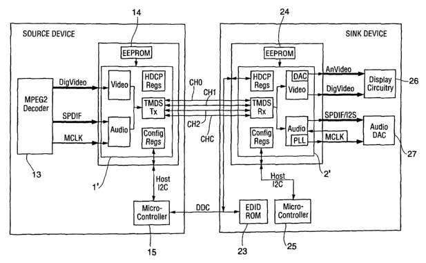
Transmitter 1' and receiver 2' of Fig. 2 correspond, respectively, to
transmitter
1 and receiver 3 of Fig. 1, but perform auxiliary data encoding, transmission,
and
decoding fiuzctions that are not performed by transmitter 1 and receiver 3 of
Fig. 1.
Transmitter 1' of Fig. 2 is an element of a source device that also includes
MPEG2
decoder 13 and microcontroller 15, coupled as shown. Decoder 13 asserts input
video
("DigVideo") to a video data processing subsystem of transmitter 1', and input
audio
data ("SPDIF") and audio reference clock ("MCLK") to an audio data processing
subsystem of transmitter 1'. Input audio SPDIF can be indicative of two or
more
streams of audio data (e.g., left and right stereo signals). EEPROM 14 stores
key values
and identification bits for use in HDCP encryption of content to be
transmitted to
receiver 2'.
Receiver 2' of Fig. 2 is an element of a sink device that also includes EDID
ROM 23, microcontroller 25, display circuitry 26, and audio digital-to-analog
converter
27 ("DAC" 27), coupled as shown. EDID ROM 23 is coupled to the DDC channel of
-17-
CA 02471536 2004-06-23
WO 03/058376 PCT/US02/38755
the TMDS link, and stores status and configuration bits which can be read by
microcontroller 15 over the DDC channel. Receiver 2' also includes an
interface (e.g.,
interface 201 of Fig. 14) for communication via the DDC channel with
microcontroller
15. Microcontroller 25 is coupled for I2C communication with receiver 2'.
EEPROM
24 stores key values and identification bits for use in HDCP decryption of
content
received from transmitter 1'.
The sink device also includes display circuitry 26 which receives analog
and/or
digital video recovered by receiver 2', and an audio digital-to-analog
converter 27
(DAC 27) which receives digital audio recovered by receiver 2'.
The Fig. 2 system preferably transmits a video clock over a conductor pair
(labeled "Channel C in Fig. 2) of the TMDS link, and also transmits a clock
for the
auxiliary data over at least one channel of the link. For example, transmitter
1'
transmits video data to receiver 2' over Channels 0, 1, and 2 (which are
identical to the
identically numbered channels of the Fig. 1 system) during active video
periods,
transmits audio data (e.g., left and right stereo signals) over one or more of
Channels 0,
1, and 2 to receiver 2' at times other than during the active video periods,
continuously
transmits a video clock (e.g., determined by the rising edges of a binary
waveform)
over Channel C, and transmits time stamp data (over one or more of Channels 0,
1, and
2) with each burst of the audio data. The time stamp data determine a clock
for the
audio data, as described in above-cited U.S. Patent Application No.
09/954,663, filed
on September 12, 2001. Receiver 2' is configured to process the time stamp
data to
regenerating the audio clock employed to transmit the audio data. Preferred
methods
and systems for regenerating a clock from transmitted time stamp data will be
described below in detail.
Typically the clock for a stream of audio data has a much lower frequency than
the pixel clock for a stream of video. However, in most applications the audio
clock
needs to be more accurate than the pixel clock, to reduce fitter. This is true
since
distortion in analog audio (that has been generated from digital audio data
having fitter)
is more easily discernible (to one experiencing the analog audio) than is the
distortion
in a displayed video program generated from digital video having the same
amount of
fitter.
-1 ~-
CA 02471536 2004-06-23
WO 03/058376 PCT/US02/38755
In the Fig. 2 system, 8-bit source words of video data are encoded into
transition-minimized 10-bit code words which are then serialized and
transmitted over
a channel medium (one of the conductor pairs identified as Channels 0, 1, and
2). In
receiver 2', each 10-bit code word is decoded back to the original 8-bit word
if no
errors are present. Each code word comprises a 9-bit base pattern (a
transition-
minimized member of a set of 29 nine-bit patterns, whose most significant bit
indicates
that the base pattern is transition-minimized, concatenated with a tenth bit
indicating
whether the eight least-significant bits of the base pattern have or have not
been
inverted in accordance with a DC balancing algorithm). In transmitter 1', each
8-bit
source word is first encoded to one of the 9-bit base patterns, and a stream
of the 9-bit
base patterns are then encoded as a stream of the 10-bit code words (in a
manner that
achieves improved DC balancing of the transmitted stream of 10-bit code
words).
However, the decoded video data can include errors (especially when the
relevant
channel has significant ISI), depending on the specific channel media and the
specific
data patterns of the transmitted serial bit stream.
If transmitter 1' and receiver 2' were operated to encode and decode the
auxiliary data in the same way that they encode and decode the video data, and
to send
both types of encoded data over the same channel of the serial link, the
decoded
auxiliary data would be subject to error at the same error rate. This error
rate can be
unacceptably high for auxiliary data (especially when the auxiliary data are
audio
data), even if it is acceptable for video data. To reduce the error rate for
the auxiliary
data, transmitter 1' can be configured to encode the auxiliary data using
"golden
words" as explained below. Optionally, transmitter 1' is configured also to
encode the
video data using "golden words" (or to be operable in a mode in which it
encodes both
the video data and auxiliary data using "golden words"). However, since data
encoded
using "golden words" (a robust subset of a "full set" of code words)
necessarily has a
lower data transmission rate than the same data encoded using the same "full
set" of
code words (assuming that both streams of encoded bits are transmitted with
the same
clock frequency). In many applications, video data cannot practically be
transmitted at
an adequate rate if encoded using golden words. Thus, typical implementations
of the
Fig. 2 system will encode auxiliary data (but not video data) using golden
words.
-19-
CA 02471536 2004-06-23
WO 03/058376 PCT/US02/38755
In a class of embodiments, the inventive transmitter and receiver distinguish
between at least three portions of each blanking interval (between active
video periods):
an initial portion (in which a "data island preamble" can be transmitted)
followed by an
auxiliary data portion (sometimes referred to as a "data island") followed by
a final
portion (in which a "video preamble" can be transmitted). Optionally, there
are two or
more data islands in a blanking interval (each comprising at least one
auxiliary guard
band word followed by a burst of a different stream of encoded auxiliary
data), an
initial portion between the falling edge of DE (at the start of the blanking
interval) and
the start of the first data island, an additional portion (including another
data island
preamble) before each subsequent data island in the blanking interval, and a
final
portion (including a video preamble) between the last data island and the next
active
video period. During the initial data island preamble of each blanking
interval,
repetitions of code words indicative of specific patterns of control bits
CTL3, CTL2,
CTL1, and CTLO, and optionally also initial bit patterns (e.g., patterns in
the time
interval labeled "Rsvd" in Fig. 5 at the staxt of the initial auxiliary
preamble of channels
CH2 and CH1) are transmitted. During the video preamble of each blanking
interval,
repetitions of code words indicative of other specific patterns of control
bits CTL3,
CTL2, CTL1, and CTLO, and optionally also initial bit patterns (e.g., patterns
in the
time interval labeled "Rsvd" in Fig. 6 at the start of the video preamble of
channels
CH2 and CH1) are transmitted. Preferably, during each data island, packets of
code
words indicative of encoded auxiliary data and guard band words are
transmitted.
As noted, two or more data islands can be transmitted consecutively (without
an
active video period between them). Also, two or more active video periods can
be
transmitted consecutively (without a data island between them), or data
islands can
alternate with active video periods.
In some embodiments, the following signals are transmitted during a video
preamble (as indicated in Figs. 3 and 6): repetitions of a code word,
"0010101011"
indicative of CTL3 =0, CTL2=0 are transmitted on CH2 (preferably after an
initial bit
pattern in the "Rsvd" interval), repetitions of the same code word,
"0010101011"
indicative of CTL1 =0, CTLO=0 are transmitted on CHl(preferably after an
initial bit
pattern), and repetitions of a code word indicative of one of the four
possible
-20-
CA 02471536 2004-06-23
WO 03/058376 PCT/US02/38755
combinations of sync bits HSYNC and VSYNC are transmitted on CHO. In typical
operation, during the final 12 pixel clock cycles of the video preamble (just
before the
0-to-1 transition of DE as shown in Fig. 6), both sync bits HSYNC and VSYNC
have
the value 0, so that the code word indicative of HSYNC = 0, VSYNC = 0 (namely
the
code word "0010101011" shown at the bottom of Fig. 6) is transmitted over the
channel CHO.
In such embodiments, the following signals are transmitted during the initial
data island preamble (as indicated in Figs. 3 and 5): repetitions of a code
word,
"1101010100" indicative of CTL3 = 0, CTL2 =1 are transmitted on CH2
(preferably
after an initial bit pattern in the "Rsvd" interval), repetitions of the code
word,
"0010101010" indicative of CTLl =1, CTLO = 0 are transmitted on CH1
(preferably
after an initial bit pattern), and repetitions of a code word indicative of
one of the four
possible combinations of sync bits HSYNC and VSYNC are transmitted on CHO.
During transmission of data over a serial link from a transmitter to a
receiver,
inter-symbol interference ("ISI") can give rise to errors that cause the
received data to
differ from the transmitted data. The rate at which such errors occur depends
on such
factors as the channel medium, and when the data are patterns of binary bits,
the
particular bit patterns that are transmitted. In preferred embodiments of the
invention,
data (e.g., audio data transmitted during data islands between active video
periods) are
encoded for transmission over a serial link with bit patterns that are less
susceptible to
ISI during transmission over the link than are the patterns determined by
conventionally encoded versions of the same data. Thus, the data are
transmitted more
reliably in these preferred embodiments, and with reduced error rate, than are
conventionally encoded versions of the same data. More specifically, in
preferred
embodiments, data are encoded using a subset (a "robust" subset) of a full set
of code
words. Typically, the code words in the full set have equal length (e.g., each
consists of
N bits). The robust subset will sometimes be referred to herein as a
"selected" or
"inventive" set of code words, and the code words in the robust subset will
sometimes
referred to as the "inventive" code words (or "golden words"). The robust
subset is
selected such that each transmitted stream of encoded data (coded using only
members
of the inventive code word set) has patterns that are less susceptible to ISI
during
-21-
CA 02471536 2004-06-23
WO 03/058376 PCT/US02/38755
transmission over the serial link than are patterns determined by a
transmitted,
conventionally encoded version of the same data (that has been coded using
code words
of the full set other than members of the inventive code word set, as well as
members of
the inventive code word set). Since there are more code words in the full set
than there
are inventive code words, fewer words of data can be transmitted over the link
per unit
time if the transmitted data are encoded using only the inventive code words
than if the
transmitted data are encoded conventionally using the full set of code words.
Encoding of data in accordance with the invention is particularly beneficial
in
applications in which the encoded data are transmitted over very long
conductors or
under other conditions in which there would otherwise be a high risk of error
due to ISI
during transmission.
In a class of embodiments, transmitter 1' is configured to encode auxiliary
data
transmitted between active video periods in accordance with the invention as
follows.
A subset of the full set of 10-bit TMDS code words is selected as the
"inventive" code
word set such that each transmitted stream of 10-bit words of encoded
auxiliary data
(consisting only of the inventive code words, sometimes referred to as "golden
words")
has a pattern that is less susceptible to inter-symbol interference than is
the pattern
determined by a transmitted stream of a TMDS-encoded version of the same data
(including not only inventive code words but also members of the full set that
are not
inventive code words).
In some embodiments, a 2M bit subset (where M < 8) of the full set of 10-bit
TMDS code words is selected to be the inventive code word set. Optionally, the
inventive code word set also includes one or more code words of the full set
that are
used as guard band words. The 17 inventive code words (each comprising 10
bits) to
be described below with reference to Figs. 3 and 4 are an example of such a 2M
bit
subset (where M = 4) supplemented by one additional guard band word. Receiver
2' is
implemented to decode each received one of the inventive 10-bit code words as
an
auxiliary data word of length M bits. Receiver 2' performs the same decoding
operations on the encoded auxiliary words received during blanking intervals
that it
performs on the conventionally encoded video words received during the active
video
periods. However, during the encoding of source auxiliary data (using the
inventive
-22-
CA 02471536 2004-06-23
WO 03/058376 PCT/US02/38755
code words), transmitter 1' does not perform the conventional DC balancing
steps that
it performs during its conventional encoding of source video data (in which
the eight
least significant bits of the "N+1"th encoded video word are inverted, and the
resulting
nine bits are concatenated with a distinctive tenth, most significant bit when
the
cumulative DC drift of the N previous encoded video words reaches a
predetermined
threshold, and otherwise does not invert the eight least significant bits of
the "N+1"th
encoded video word and instead concatenates the word with another distinctive,
tenth,
most significant bit). Rather, transmitter 1' is configured simply to replace
each 4-bit
source word of auxiliary data with the corresponding one of the inventive code
words,
regardless of the cumulative DC drift of the resulting stream of inventive
code words
(and regardless of whether the MSB of the inventive code word is a one or
zero). The
inventive code words are preferably chosen so that when the bits of a stream
of the
inventive code words are transmitted over a serial link as sequence of rising
and falling
voltage transitions, the bit pattern of such stream of the inventive code
words is DC
balanced (or is likely to be DC balanced) in the sense that the voltage drift
that it
determines over time is limited to an acceptable amount.
In other embodiments, transmitter 1' does perform the same DC balancing steps
during its encoding of source auxiliary data (using the inventive code words)
and
during its conventional encoding of source video data. This is taken into
consideration
in the selection of the inventive code word set. Specifically, each code word
of the
inventive code word set has a 9-bit base pattern that is a member of a
selected subset of
the 9-bit base pattern space of the full set of 10-bit TMDS code words, and
during
encoding of 4-bit words of source auxiliary data (to replace them with the
inventive 10-
bit code words), the eight least-significant bits of this 9-bit base pattern
are either
inverted and the resulting pattern concatenated with a tenth (and most
significant) bit
having a first value, or the base pattern is not inverted and is instead
concatenated with
a tenth (and most significant) bit having a second value, depending on whether
the
cumulative DC drift of the stream of previously encoded auxiliary words has
reached a
predetermined threshold. In these embodiments, receiver 2' is implemented to
perform
the same decoding operations on the encoded auxiliary data words received
during
blanking intervals that it performs on the conventionally encoded video data
words
-23-
CA 02471536 2004-06-23
WO 03/058376 PCT/US02/38755
received during the active video periods, and then to map each 8-bit word
(generated as
a result of conventional decoding of one of the 10-bit encoded auxiliary data
words) to
one of the 2M auxiliary data words each having M-bit length.
In the described embodiments of the Fig. 2 system, the size of the auxiliary
data
encoding space (the number of different auxiliary data words that can be
encoded with
the inventive code word set) is reduced from 28 (= 256) to 2M (where M < 8) in
accordance with the invention, and thus the effective rate at which the
auxiliary data
(encoded in accordance with the invention) can be transmitted is reduced from
8 bits
per clock period per channel to M bits per clock period per channel. By
reducing the
value M (i.e., selecting a smaller inventive set of code words from the full
set), a lower
bit-error rate (BER) can be achieved but the data rate will also be reduced.
Conversely,
increasing the parameter M results in an increased data rate but at the cost
of increased
BER.
We next describe an embodiment of the inventive code word set with reference
to Figs. 3 and 4. This code word set is a subset of the full set of
conventional TMDS
10-bit code words, and is useful for encoding 4-bit words of auxiliary data
for
transmission over a TMDS (or TMDS-like) link over which 8-bit video words
(conventionally encoded using the full set of TMDS 10-bit code words) are also
transmitted, in cases when it is adequate to transmit the auxiliary data at
half the data
rate as the video data. Typically, 8-bit input words of binary auxiliary data
are
buffered, the four least-significant bits of each are encoded (e.g., in
transmitter 1' of
Fig. 2) as one of the sixteen 8-bit words "ADO-AD15" in the left column
(labeled
"Input D7-DO") of Fig. 4, and the four most significant bits of each 8-bit
input word are
also encoded as the appropriate one of the sixteen 8-bit words ADO-AD15. Each
of the
words ADO-AD 15 has the hexadecimal representation shown in Fig. 4 in the
second
column from the left. Each of the words ADO-AD15 is then encoded (e.g., in
transmitter 1') as the corresponding one of the 10-bit patterns shown in the
third
column (labeled "TMDS result") of Fig. 4. We shall describe the other columns
of Fig.
4 below, with reference to the aspects of the invention that pertain to the
mapping of
code word clusters.
-24-
CA 02471536 2004-06-23
WO 03/058376 PCT/US02/38755
In Fig. 4 (and Fig. 3), the left bit of each code word is the LSB and (in the
case
of each 10-bit code word) is the first bit to be transmitted over the serial
link. Also, the
right bit of each code word is the MSB and (in the case of each 10-bit code
word) is the
last bit to be transmitted over the serial link.
For example, an input auxiliary data word 10000000 (whose LSB is 1) would
be split into two halves (1000 and 0000) and the two halves then encoded as
AD1 and
ADO, respectively. Then, the 8-bit word ADO is encoded as the 10-bit inventive
word
"0011100101" and the 8-bit word AD1 is encoded as the 10-bit inventive word
"0110001101." The two inventive words would then be serialized transmitted
over the
serial link sequentially, with the bits "0011100101" indicative of the "most
significant"
half (0000) of the input word being transmitted before the bits "0110001101"
that are
indicative of the least significant half (1000) of the input word. At the
receiver, each
10-bit inventive word is decoded into one of the 8-bit words ADO-AD15, and the
original 8-bit input auxiliary data words can be reconstructed from the
recovered words
ADO-AD15 since there is a one-to-one mapping between each word ADO-AD15 and
one half (four bits) of each 8-bit input auxiliary data word.
Of course, the input auxiliary data asserted to the transmitter (e.g.,
transmitter
1') can be 4-bit words, in which case the transmitter would not need to split
(or
otherwise pack) received input auxiliary data words into 4-bit format before
encoding
them as a sequence of the words ADO-AD15. Alternatively, the input auxiliary
data
can be pre-encoded as a sequence of 8-bit words ADO-AD15, and the pre-encoded
auxiliary data then provided to the transmitter in the form of a sequence of
the 8-bit
words ADO-AD15.
Typically, the encoded auxiliary data are transmitted in the same channels
(CHO, CHl, and CH2) of a TMDS link in which video data are transmitted, but
the
auxiliary data are transmitted during the blanking intervals between the
active video
periods of video data transmission. Figs. 5 and 6 are timing diagrams of
signals
transmitted during such an embodiment of the invention. The upper nine signals
of
Fig. 5 represent signals input to the transmitter during a control data period
and data
island (of a blanking interval), and the lower three signals of Fig. 5
represent the
auxiliary data (encoded using the 10-bit words of Fig. 4) and encoded control
and sync
-25-
CA 02471536 2004-06-23
WO 03/058376 PCT/US02/38755
signals (to be discussed below) that are transmitted over channels CHO, CHl,
and CH2
during the control data period and data island in response to the upper nine
signals.
Similarly, the upper nine signals of Fig. 6 represent signals input to the
transmitter in a
control data period at the end of a blanking interval (the blanking interval
of Fig. 5) and
during the active video period that follows such control data period, and the
lower three
signals of Fig. 6 represent the auxiliary data (encoded using the 10-bit words
of Fig. 4),
video data (conventionally encoded), and encoded control and sync signals (to
be
discussed below) that are transmitted over channels CHO, CHl, and CH2 in
response to
the upper nine signals.
In Figs. 5 and 6:
24-bit words of input data are provided to the encoding circuitry of the
transmitter for encoding. Fig. 5 pertains to those of such words (each
identified as
D[23:0] in Fig. 5) that are words of auxiliary data. Fig. 6 pertains to those
of such
words (each identified as D[23:0] in Fig. 6) that are words of video data.
Eight bits of
each input word (D[23:16]) are encoded, serialized, and transmitted on channel
CH2
(as 10-bit encoded words CH2[0:9]), another eight bits of each such word
(D[15:8]) are
encoded, serialized, and transmitted on channel CH1 (as 10-bit encoded words
CHl [0:9]) and another eight bits of each such word (D[7:0]) are encoded,
serialized,
and transmitted on channel CHO (as 10-bit encoded words CHO[0:9]). In some
implementations, the video data are in RGB format (and the red, green, and
blue pixels
are transmitted on channels CH2, CH1, and CHO, respectively). In view of this,
channels CH2, CH1, and CHO, are sometimes referred to herein (such as in Fig.
3) as
the red (or "R") channel, the green (or "G" channel), and the blue (or "B")
channel,
respectively. Alternatively, the video data that are encoded (and then
transmitted) are
in luminance-chrominance format;
the waveform "DCK" indicates the data clock. During each cycle of the data
clock, the ten bits of each one of the inventive code words indicative of
auxiliary data
(or a guard band), or each of the conventional TMDS 10-bit code words
indicative of
video data, are sequentially transmitted over the relevant one of channels
CHO, CHl,
and CH2. In some actual implementations, phase shifting circuitry is used to
generate
multiple, phase-shifted versions of the clock DCK which are then used (with
the clock
-26-
CA 02471536 2004-06-23
WO 03/058376 PCT/US02/38755
DCK itself) to clock the encoding, transmission, and decoding operations. In
other
actual implementations, a clock having ten times the frequency of DCK (but in
phase
with DCK) could be used to clock the encoding, transmission, and decoding
operations,
and one code bit would be transmitted during each cycle of this faster clock;
the waveform "DE" (of Fig. 6) is the video data enable signal, and the
waveform "AUX DE" (of Fig. 5) is the auxiliary data enable signal. When DE =1
and
AUX DE = 0, video data (identified as D[23:16], D[15:8], and D[7:0] in Fig. 6)
are
encoded, and serialized 10-bit words of the encoded video are transmitted over
channels CHO, CHl, and CH2. When DE = 0 and AUX DE =1, auxiliary data
(identified as D[23:16], D[15:8], and D[7:0] in Fig. 5) are encoded, and
serialized 10-
bit words of the encoded auxiliary data are transmitted over channels CHO,
CH1, and
CH2. When DE = 0 and AUX DE = 0, the transmitter ignores signals asserted to
its
data inputs and instead encodes (as 10-bit TMDS code words) control bit pairs
asserted
to its control inputs (bits CTL3 and CTL2, indicated as "CTL[3:2]" in Figs. 5
and 6,
and bits CTL1 and CTLO, indicated as "CTL[1:0]" in Figs. 5 and 6), serializes
these
code words, and transmits the serialized code words over channels CH1 and CH2.
In a
DVI system, the transmitter encodes (as 10-bit transition-maximized words)
sync bit
pairs (HSYNC and VSYNC) asserted to its sync inputs, serializes these code
words,
and transmits the serialized code words over channel CHO when DE = 0. However,
in
preferred embodiments of the present invention, during each data island, a 10-
bit
transition-minimized code word indicative of HSYNC and VSYNC is sent each
pixel
clock cycle (e.g., one code word indicative of an HSYNC bit, a VSYNC bit, and
two
other bits is sent per pixel clock cycle) over channel CHO. In this way, HSYNC
and
VSYNC can be transmitted repeatedly over the 32-pixel clock period required to
send a
packet during a data island. Preferably, each packet sent during a data island
includes a
32-bit packet header, and each code word indicative of HSYNC and VSYNC that is
transmitted during a data island is also indicative of one bit of the packet
header. Thus,
32 pixel clock cycles are required to transmit an entire 32-bit packet header.
Although Figs. 5 and 6 have been described with reference to two data enable
signals, "DE" and "AUX DE," it is contemplated that the inventive transmitter
can be
implemented with a portion (e.g., "core" processor 114 of transmitter 100 of
Fig. 13)
-27-
CA 02471536 2004-06-23
WO 03/058376 PCT/US02/38755
configured to perform all the described encoding, serialization, and
transmission in
response to a single data enable signal (e.g., a combined enable signal
indicative of the
result of performing a logical "OR" operation on the signals DE and AUX DE),
and a
single set of data inputs (D[23:0]) indicative of either video or auxiliary
data.
Additional circuitry of the transmitter outside the core is configured to
receive separate
sets of auxiliary data (e.g., 24-bit auxiliary data words) and video data
(e.g., 24-bit
video data words), and both a video data enable signal DE, and an auxiliary
data enable
signal "AUX DE." The data enable signals can have the following repeating
sequence
of values: (DE = 0, AUX DE = 0), then (DE =1, AUX DE = 0), then (DE = 0, AUX
DE = 0), and then (DE = 0, AUX DE = 1). Of course, the data enable signals can
also
occur with other sequences of values, including non-repeating sequences. For
example,
in some circumstances, auxiliary data are transmitted in some but not all
video blanking
intervals. Thus, auxiliary data can be transmitted in one blanking interval
but not the
next blanking interval, with the signals DE and AUX DE having the following
sequence of values: (DE = 0, AUX DE = 0), then (DE =1, AUX DE = 0), then (DE =
0, AUX DE = 0), then (DE = 0, AUX DE =1), then (DE = 0, AUX DE = 0), then (DE
=1, AUX DE = 0), then (DE = 0, AUX DE = 0), and then (DE =1, AUX DE = 0). The
additional circuitry of the transmitter can include logic circuitry that "ORs"
together the
signals DE and AUX DE to produce a combined data enable signal. The additional
circuitry can also pack the auxiliary data into 4-bit format, encode each 4-
bit portion of
the auxiliary data as one of the words ADO-AD15 shown in Fig. 4, add guard
band
words with appropriate timing into the stream of ADO-AD15 auxiliary data
words, and
add video guard band words into the stream of video data (or alternatively
replace, with
appropriate timing, words of the video data with video guard band words). The
additional circuitry can assert a sequence of bursts of the video data (with
video guard
band words) and auxiliary data (with guard band words) to the core (e.g.,
alternating
bursts of the video data with video guard band words, and auxiliary data with
guard
band words), and also assert the combined data enable signal to the core. The
core
performs all the encoding, serialization, and transmission operations
described with
reference to Figs. 5 and 6 in response to the combined data enable signal
(rather than
separate DE and AUX DE signals) and the bursts of video and auxiliary data.
-2~-
CA 02471536 2004-06-23
WO 03/058376 PCT/US02/38755
In variations on the embodiments described in the previous paragraph, the
"additional circuitry" of the transmitter is coupled and configured to receive
and encode
two or more sets of auxiliary data (each set comprising a different type of
auxiliary
data). The additional circuitry is also coupled and configured to receive a
set of video
data, an auxiliary data enable signal for each set of auxiliary data (e.g.,
first and second
auxiliary data enable signals "AUX1 DE" and "AUX2 DE") and a video data enable
signal ("DE"), and to assert a sequence of bursts of the video data and bursts
of the
encoded auxiliary data to the transmitter's core. The video data enable signal
("DE")
and auxiliary data enable signals ("AUXl DE" and "AUX2 DE") can have the
following repeating sequence of values: (DE = 0, AUXl DE = 0, AUX2 DE = 0),
then
(DE =1, AUX1 DE = 0, AUX2 DE = 0), then (DE = 0, AUXl DE = 0, AUX2 DE = 0),
then (DE = 0, AUXl DE = l, AUX2 DE = 0), and then (DE = 0, AUXl DE = 0, AUX2
DE =1). The additional circuitry can include logic circuitry that "ORs"
together the
signals DE, AUX1 DE, and AUX2 DE to produce a combined data enable signal, and
can assert the combined data enable signal (rather than the individual video
data enable
and auxiliary data enable signals) to the core.
In each of at least one channel of a serial link (e.g., in each of channels
CH2 and
CH1 in the case of data transmission in accordance with the invention over a
TMDS
link), an appropriate one of the inventive code words is (or two or more
appropriate
ones of the inventive guard band words are) preferably transmitted (as a guard
band
word or set of guard band words) at the start of each burst of encoded
auxiliary data
(i.e., immediately after each "auxiliary preamble" of each blanking interval),
at the end
of each burst of encoded auxiliary data, and at the start of each burst of
encoded video
data (i.e., immediately after the "video preamble" of each blanking interval).
In preferred embodiments of the invention, the source data to be transmitted
during data islands are encoded using a "robust" subset of a full set of code
words.
Each "robust" subset consists of code word sets (sometimes referred to herein
as
"golden sets"), with each golden set consisting of one or more code words
(sometimes
referred to herein as "golden words"). Each "golden word" of a golden set is
indicative
of a single source data value (e.g., a source data word). In the case that a
golden set
consists of two or more golden words, each of these golden words is indicative
of the
-29-
CA 02471536 2004-06-23
WO 03/058376 PCT/US02/38755
same source data value. Clusters of code words in the full set are determined.
Each
cluster includes a "golden set" and optionally also one or more additional
code words
of the full set, where each of the additional code words is "similar" to a
golden word of
the cluster's golden set in the sense that each additional code word is likely
to be
generated as a result of probable bit errors in transmission, or transmission
and
decoding, of such golden word. Each received code word in one of the clusters
is
mapped to the source data value determined by the cluster's golden set. Each
mapping
of a cluster of received code words to a single source data value can provide
error
correction by mapping an error-containing word in the cluster back to the
source data
value most likely to correspond to the error-containing word.
The full set of code words can be used to encode one type of data (e.g., video
data) for transmission over a channel of a serial link, and the robust subset
can be used
to encode another type of data (e.g., audio data or other "auxiliary" data
related to or
useful with video data) for transmission over the same channel.
In some embodiments, each code word in each golden set (and each code word
in the full set) is an N-bit word that is an encoded version of an M-bit word,
where M is
an integer less than N. After transmission of a sequence of N-bit golden words
over the
serial link, each received N-bit code word can differ from one of the golden
words (if a
transmission error has occurred) or it can be identical to one of the
transmitted golden
words. Each received N-bit code word in one of the clusters is decoded to
generate a
decoded M-bit word, and each such decoded M-bit word is mapped to the source
data
value determined by the cluster's golden set.
For example, in a class of embodiments, the full set of code words is the set
of
10-bit, transition-minimized TMDS-encoded words that are indicative of 256
eight-bit
source words. The robust subset of the full set consists of eight-bit "golden
words"
indicative of a subset of the full set of 256 eight-bit source words. In
preferred
embodiments in this class, the robust subset consists of sixteen golden sets,
each
golden set consists of the 10-bit TMDS code words indicative of one eight-bit
source
word, and each cluster of the 10-bit TMDS code words includes one of the
golden sets
and at least one 10-bit TMDS code words similar to the code words in such
golden set.
In such preferred embodiments, each received 10-bit code word in one of the
clusters is
-30-
CA 02471536 2004-06-23
WO 03/058376 PCT/US02/38755
decoded in accordance with the TMDS decoding algorithm (or a modified version
thereof) to recover an eight-bit word, and each recovered eight-bit word is
mapped to
the eight-bit source word determined by the cluster.
With reference to Fig. 7, we will fiuther describe the concept of mapping of
clusters (e.g., clusters Sa and Sb in Fig. 7) of received words to individual
transmitted
source data words (e.g., words "a" and "b") that is employed in preferred
embodiments
of the invention. Then, we will describe a specific example of such mapping
with
reference to Fig. 4.
With reference to Fig. 7, the full set of code words (which can be used to
encode primary data, for example when auxiliary data are encoded in accordance
with
the invention using only "golden words" of the full set) are those code words
(the "2N
space") that can be used to encode 2N different source data words, each source
data
word being an ordered set of N bits. The golden words (the "2" space") are a
subset of
the code words of the full set that can be used to encode 2" different source
data words,
each such source data word being an ordered set of "n" bits (where "n" is an
integer
less than N). Initially, raw source data (which can consist of words of any
length) can
be buffered and packed into an n-bit format (i.e., into n-bit members of a set
of 2"
source data words). Each different n-bit source data word can then be encoded
as one
of the golden words (in the "2" space") and transmitted over a serial link
(typically over
a single channel of the link). The transmission can result in error or it can
be error free.
Clusters of the full set of code words are predetermined such that each
cluster
includes a "golden set" (of one or more of the golden words) and optionally
also one or
more additional code words of the full set, where each of the additional code
words is
similar to a golden word of the cluster's golden set. In Fig. 7, for example,
cluster "Sa"
includes the golden set consisting of each of the golden words that encodes
source
word "a," and cluster "Sb" includes the golden set consisting of each of the
golden
words that encodes source word "b"). Each received code word in one of the
clusters is
mapped to the source data value determined by the cluster's golden set.
In some embodiments in which N = 8 and n = 4, each code word of the 2N space
is a 10-bit TMDS-encoded word, and the 2n space is a subset of the full set of
10-bit
TMDS-encoded words. Each transmitted 10-bit T1VIDS code word is decoded in
-31-
CA 02471536 2004-06-23
WO 03/058376 PCT/US02/38755
accordance with the TMDS decoding algorithm (or a modified version thereof) to
generate an 8-bit code word. In these and other embodiments of the invention,
the
transmission of golden words (and any decoding thereof) can result in error or
can be
error free.
For each specific golden word, certain types of transmission errors can be
expected when the channel has inter-symbol interference or other degradations.
Thus,
for each golden word (i.e., for each N-bit member of the 2" space), the
cluster
containing such golden word preferably includes all the N-bit members of the
2" space
likely to result from occurrence of such a transmission error during
transmission of the
golden word. However, since the clusters are disjoint, an N-bit word included
in one
cluster is omitted from all the other clusters.
Each embodiment of the invention employs at least one (and typically more
than one) cluster that contains at least one code in addition to each golden
word of a
golden set. Some embodiments of the invention employ at least one cluster that
contains at least one code in addition to each golden word of a golden set,
and also at
least one other cluster that contains no code other than each golden word of a
golden
set. Since all the clusters (e.g., Sa, Sb, etc. of Fig. 7) are mutually
disjoint, then
regardless of whether or not an error occurs during transmission (or
transmission and
decoding), if a cluster contains a received N-bit code, the received code is
mapped back
to the correct source word.
In a class of implementations of Fig. 7, the full set of code words (the "2N
space") is the full set of 10-bit TMDS code words, and the "2n space" consists
of those
TMDS code words that are indicative of a predetermined set of 16 different 8-
bit source
data words. Thus, each cluster includes a golden set of the TMDS code words
including golden words indicative of one of the 16 different source data
words.
Typically, 4-bit words of raw source data are preliminarily encoded as the 16
different
8-bit source data words, and each resulting 8-bit source data word is then
encoded as
one of the 10-bit members of the 2" space for transmission. Thus, the robust
subset (of
the full set of TMDS code words) consists of those 10-bit TMDS code words that
(when decoded in accordance with the TMDS decoding algorithm or a modified
version thereof) determine the 16 predetermined 8-bit source data words (of
the 256
-32-
CA 02471536 2004-06-23
WO 03/058376 PCT/US02/38755
eight-bit source data words determined by the full set of TMDS code words).
Each
cluster preferably includes not only the golden words of a golden set, but
also at least
one 10-bit TMDS code word "similar" to one of the golden words in the sense
that it is
more likely to result from bit errors in transmission of the golden word than
are other
TMDS code words (e.g., the code word "similar" to the golden word may differ
from
the golden word only in the value of one of its bits).
The process of selecting the golden sets from the full set of code words is
very
important. In general, the best choice for the specific golden sets selected
from a full
set of binary code words depends on the particular coding implemented by the
full set
(i.e., the details of which bits of each code word in the full set are zeroes
and which are
ones). As noted above, in some preferred embodiments, the code words of the
golden
sets are selected to be those whose serial patterns (during transmission) have
fewer
contiguous zeros and ones (e.g., on the average), and thus are less
susceptible to ISI
during transmission, than do those code words in the full set that are not
selected (e.g.,
the average number of contiguous zeros and ones, per code word, of the golden
words
is less than the average number of contiguous zeros and ones, per code word,
of the
code words in the full set that are not selected as golden words).
In other preferred embodiments, the golden words are selected to be those
satisfying the criterion that the Hamming distance between any golden word in
one
cluster and any golden word in any other cluster exceeds a threshold, or the
criterion
that the Hamming distance between golden words in different clusters is
maximized (in
some sense) to the extent practical (e.g., the criterion that an average
Hamming
distance between golden words in different clusters is maximized) subject to
the
constraint that the clusters are mutually disjoint. This helps to increase the
number of
"errored codes" (codes other than golden codes of one golden set) that can be
included
in each cluster, while keeping the constraint that the clusters are mutually
disjoint.
To implement the invention, the receiver (e.g., receiver 200 of Fig. 14) is
preferably configured to include a predetermined table that outputs one value
(e.g., a
source data word) determined by each cluster in response to each input
indicative of an
element of the cluster (e.g., in response to each of four received code words,
where the
cluster consists of one golden word and three code words similar to the golden
word).
-33-
CA 02471536 2004-06-23
WO 03/058376 PCT/US02/38755
The table implements a mapping of each received code word in each cluster to
the
source word determined by the cluster's golden set, or of each received code
word in
each cluster to a golden word of the cluster's golden set (which is then
mapped by
conventional hardware or software in (or external to) the receiver to a source
word
determined by the cluster's golden set), or of a decoded version of each
received code
word in each cluster to a source word determined by the cluster's golden set,
or of a
decoded version of each received code word in each cluster to a single decoded
code
word (which is then mapped by conventional hardware or software in, or
external to,
the receiver to a source word determined by the cluster's golden set).
For example, receiver 200 of Fig. 14 includes core processor 214 (which
includes code word recovery circuitry), and mapping and decoding circuitry 20
(of
subsystem 208) which implements such a table. Circuitry 214 is configured to
recover
10-bit TlVmS code words from the data received on each of TlVmS channels CHO,
CH1, and CH2. Circuitry 20 is configured to map each recovered word in one of
the
clusters to a golden word of the cluster (using the table), to decode each
golden word to
generate an 8-bit decoded value (one of the seventeen 8-bit words in the left
column of
Fig. 4). The 8-bit decoded values are indicative of source words. Although in
some
embodiments of the invention, mapping and decoding circuitry would generate a
4-bit
raw source data word in response to each decoded 8-bit word (indicative of one
of the
words ADO-AD15 in Fig. 4), circuitry 20 of Fig. 14 asserts 8-bit decoded words
to
decryption circuitry 21.
The clusters (and thus the inputs to the above-mentioned table in the
receiver)
can be a partition of the full set of code words (e.g.~, the 2N space of Fig.
7), so that the
union of the clusters covers the whole space of code words (e.g., the entire
2N space of
Fig. 7) and the clusters are mutually disjoint. However, when the probability
that one of
the code words in the full set will be received in response to transmission of
one golden
word is very small or negligible, then such code word can be excluded from all
of the
clusters (and dropped from the table). In the latter case, the union of the
clusters does
not cover the whole space of code words (e.g., the entire 2N space of Fig. 7).
For convenience, in the claims, we use the expression "to map each code word
of a cluster to the input data (or source data) value determined by the
cluster's preferred
-34-
CA 02471536 2004-06-23
WO 03/058376 PCT/US02/38755
word set (or golden set)," or variations on this expression, to denote the
mapping of
each code word of a cluster directly to the source data (input data) value
determined by
the cluster's preferred word set (golden set), or the mapping of each code
word of a
cluster to a golden word (or preferred word) of the cluster's golden set (or
preferred
word set) optionally followed by conventional mapping of the golden word (or
preferred word) to the source data (input data) value determined by the
cluster's golden
set (or preferred word set), or the mapping of a decoded version of each code
word of a
cluster to the source data (input data) value determined by the cluster's
golden set (or
preferred word set), or the mapping of a decoded version of each code word of
a cluster
to a single decoded code word optionally followed by conventional mapping of
the
decoded code word to a source data (input data) value determined by the
cluster's
golden set (or preferred word set).
The mapping of words in each cluster to a golden code can be performed in a
manner that is in some sense "on the fly," for example using clocked logic to
substitute
a golden code for each received word that belongs to a predetermined cluster
that
contains the golden code. For example, in some embodiments, the receiver
includes
logic (e.g., in circuitry 20 of Fig. 14) that applies rules to determine which
one of the
bits of a received code word is likely to be erroneous, and then "map" the
received code
word to a golden code by flipping each bit that it determines to be likely to
be errored.
Alternatively, the mapping of words in each cluster to a golden code is
performed using
a look-up table which outputs a golden code in response to each word of a
cluster that
contains the golden code.
In general, an algorithm can be implemented (e.g., by software or logic
circuitry) to determine which bits (to be referred to as "vulnerable" bits) in
a golden
word are most vulnerable to error, a process is then implemented wherein
vulnerable
bits of golden words are replaced by errored versions thereof to determine
"likely error-
containing code words," and a process is then implemented to compare all (or a
subset
of all) of the "likely error-containing code words" to the actual received
code words
and thereby to map each received code word that is a "likely error-containing
code
word" to the corresponding golden word. The algorithm for identifying
vulnerable bits
-35-
CA 02471536 2004-06-23
WO 03/058376 PCT/US02/38755
preferably identifies bits that are most susceptible to inter-symbol
interference. Single
'0' bits within a stream a '1' bits would qualify.
Once the vulnerable bits are found, they are flipped in the golden words,
thereby producing "likely error-containing code words". Either a single
vulnerable bit
could be flipped or more than one, depending upon how vulnerable to error each
of
them is. An alternative approach is to determine manually which bit patterns
include
vulnerable bits and store a series of masks with each bit pattern that the
designer wishes
to address, along with the golden words. Logic would then only need to flip
the
relevant bits in the golden words to generate the "likely error-containing
code words."
The process of choosing which code words to include in each cluster can be
automated using logic circuitry (or software). For example, it can be
systematically
determined using software (or logic circuitry) which bits of a set of golden
words are
likely to be inverted (or dropped) as a result of error in transmission and/or
recovery,
and the most likely error-containing versions of each golden word then
included in a
cluster with the golden word. For another example, for each code word already
included in a cluster, four additional code words can be automatically added
to the
cluster: two left-shifted versions of the code word (one with "0" in the
opened spot; the
other with "1" in the opened spot); and two right-shifted versions of the code
word (one
with "0" in the opened spot; the other with "1" in the opened spot), subject
to
application of rules to avoid assigning the same code word to two different
clusters.
Although the clusters should strictly be disjoint, two or more clusters can
conditionally include the same code word (to be denoted as a "mufti-value"
code word
for convenience), where a mufti-value code word is "conditionally included" in
a
cluster in the sense that it is mapped to the cluster's golden word only
provided that a
predetermined condition is met. The conditions associated with the mufti-value
code
word in the different clusters should differ from each other, and should be
chosen such
that only one of the conditions can be met in any particular case, so that a
receiver will
be able to map the mufti-value code word to one specific cluster's golden word
in each
particular case. In such embodiments, the receiver would apply predetermined
rules to
pre-existing information to determine which of the conditions is met in each
particular
case. For example, assume that a received error-containing word "A" was most
likely
-36-
CA 02471536 2004-06-23
WO 03/058376 PCT/US02/38755
transmitted as word "B" under condition "X," and was most likely transmitted
as word
"C" under a different condition "Y." A first cluster includes word "B" and
conditionally
includes word "A" (subject to condition "X"). A second cluster includes word
"C" and
conditionally includes word "A" (subject to condition "Y"). In this example,
the
receiver would apply an algorithm to pre-existing information to determine
which of
conditions X and Y is met during transmission of the code words. For instance,
the
receiver could determine whether the bit pattern of a stream of the "Z" most
recently
inventive code words (where Z is a number) is DC balanced, and determine that
condition X (but not condition Y) is met if the bit pattern is DC-unbalanced
in the
positive direction, and that otherwise condition Y (but not condition X) is
met. In this
example, the pre-existing information is the DC-balance level of the specified
bit
pattern. Alternatively, the pre-existing information could be a history of
types of
errors, or the pixel clock frequency, or a type of fitter, or other
information.
Since a large number of possible errors can occur, it is possible that
predicted
errors that are likely to affect transmission of two different golden words
(of two
different golden sets) will produce the same received code. This could
undesirably
cause an overlap in the clusters including the two golden sets, unless one of
the clusters
is predetermined to exclude the received code (or unless the received code is
conditionally included in two or more clusters, as described in the previous
paragraph).
To avoid such overlap between clusters, the received code that is less likely
to occur is
preferably excluded from the relevant cluster. For example, if a first cluster
includes a
first golden word, a second cluster includes a second golden word, a received
code
word (that is not a golden word) is expected (with probability P1) to result
from
transmission of the first golden word, and the same received code word is
expected
ZS (with probability P2, where P2 is less than P1) to result from transmission
of the second
golden word, then the first cluster should include the received code word, but
the
received code word should not be included in the second cluster.
Consider for example the case that a received error-containing word "A" is
most
likely to have been transmitted as golden word "B" and slightly less likely to
have been
transmitted as word "C" (where word "B" differs from word "C" by only one
bit). In a
class of preferred embodiments, two disjoint clusters containing code words A,
B, and
-37-
CA 02471536 2004-06-23
WO 03/058376 PCT/US02/38755
C are determined as follows: a first cluster including golden word B and word
A (and
typically other words similar to B); and a second cluster including golden
word C and
one or more other words similar to C that are not included in the first
cluster. With the
clusters determined in this way, only a single bit error would result from
transmission
of word C, reception of word A (as a result of error in transmission and/or
reception of
the transmitted word C), and mapping of the received word A to golden word B.
Preferably, the receiver includes error correction circuitry (ECC), and the
receiver is
configured to assert to the ECC the code words that result from mapping of
received
words (belonging to the clusters) to golden words. In the appropriate cases,
the ECC
would replace a word B in a block of code words by the word C. For example, if
the
ECC determines that such a word B has a bad bit, and the word B would be
transformed to word C by flipping this bit, then if the bit is the only bad
bit for the
entire ECC block, the ECC could correct the error by flipping the bad bit and
thereby
transform the word B to the word C.
As noted, some implementations of the inventive receiver are configured to
perform a two-stage mapping of received versions of the golden words to source
data
values: a first stage in which each received code word in a cluster is mapped
to a
golden word of the cluster's golden set; and a second stage in which the
golden words
determined during the first stage is mapped to the source word determined by
the
cluster's golden set. In some such implementations, an additional block of
error
correction code is transmitted with each set of golden words, and the receiver
is
configured to perform the first stage of mapping before performing error
correction
using the error correction code (to correct error-containing received code
words that are
not members of any of the clusters, to replace them with golden words to the
extent
possible). In the latter implementations, the inventive golden words and
clusters are
preferably chosen so as to implement mappings that exploit the degree of
freedom
provided by the performance of error correction. For example, the golden words
can be
selected to satisfy the criteria that the Hamming distance between any two
golden
words in different clusters is minimized to the extent practical (or otherwise
not
maximized), and that the clusters are mutually disjoint. With clusters
including such
golden words, the number of erroneous bits detected by the error correction
circuitry in
-38-
CA 02471536 2004-06-23
WO 03/058376 PCT/US02/38755
the receiver can be minimized and hence, the overhead of the error correction
code can
be minimized.
For example, receiver 200 of Fig. 14 includes decryption circuit 21 which
receives and decrypts 8-bit decoded words from "mapping and decoding"
circuitry 20,
and error correction circuitry 22 coupled to receive the decrypted, decoded
words
output from circuit 21. Circuitry 20 is configured to perform a first stage of
mapping to
generate (and assert to circuit 21) a golden word in response to each
recovered code
word that is a member of one of the inventive clusters, but errors in some
recovered
words may prevent circuitry 20 from mapping the error-containing recovered
words to
golden words. Decrypted versions of the golden words determined by circuitry
20, the
error-containing recovered words, and error correction code recovered with the
code
words are asserted to error correction circuitry 22. Circuitry 22 can pass
through the
decrypted golden words that it receives, and perform error correction using
the error
correction code to correct error-containing code words that are not members of
any of
the inventive clusters, thereby replacing such error-containing code words
with golden
words to the extent possible. In variations on the described implementation of
receiver
200, error correction is not performed and circuitry 22 is omitted.
With reference to Fig. 4, we next describe a specific example of a set of
seventeen golden words and a set of code word clusters (each including one of
the
golden words) employed in a class of preferred embodiments of the invention.
In Fig.
4, the third column (from the left) shows the seventeen golden words, which
have been
described above. Sixteen of the golden words are used to encode sixteen
different 8-bit
source data words (each 8-bit source data word being indicative of four bits
of raw
source data), and the other golden word (the word "1100110010" in the first
row) is
used only as a guard band word. Each of the golden words is a 10-bit TlVmS
encoded
word. The fourth column (from the left) shows some possible error cases for
each 10-
bit golden word, the fifth column shows the 8-bit word resulting from decoding
of the
corresponding 10-bit word in the fourth column in accordance with the
conventional
TMDS decoding algorithm, and the sixth column simply shows the hexadecimal
representations of the corresponding elements in the fifth column. The seventh
column
(from the left) includes an indication as to whether each corresponding word
in the
-39-
CA 02471536 2004-06-23
WO 03/058376 PCT/US02/38755
fourth column is or is not a member of the cluster containing the
corresponding golden
word in the third column. Specifically, the term "IGNORE" in the seventh
column
indicates that the corresponding word in the fourth column is not a member of
the
cluster that contains the corresponding golden word in the third column.
There are seventeen clusters (separated by the horizontal bars in Fig. 4): a
first
cluster including the golden word "1100110010" and the code words "1110110010"
and "1100010010" (all mapped to the "pre-data" auxiliary guard band word
"01010101"); a second cluster (for encoding the source word ADO) including the
golden word "0011100101" and the code words "1011100101," "0001100101,"
"0011110101,"and "0011100001" (all mapped to the source word ADO); a third
cluster
(for encoding the source word AD1) including the golden word "0110001101" and
the
code words "0111001101" and "0110000101" (all mapped to the source word AD1);
and the fourteen other indicated clusters (each including a different one of
the fourteen
other golden words, and consisting of words mapped to a different one of the
source
words AD2-AD 15).
When the receiver recovers a code word (in the fourth column of Fig. 4) in one
of the indicated clusters (there will be no "IGNORE" symbol in the seventh
column
corresponding to such recovered code word), the receiver will map the
recovered code
word to the source word (in the first column of Fig. 4) determined by the
cluster's
golden word (which is equivalent to mapping the recovered code word to the
cluster's
golden word in the third column).
Those code words in the fourth column marked with the term "IGNORE" in the
seventh column are not members of the cluster that contains the corresponding
golden
word. For example, the code word "1100111010" in the third row of Fig. 4 is
not a
member of the first cluster (containing golden word "1100110010") because this
code
word is a member of the cluster that contains golden word "1000111010" and the
clusters should be disjoint. Although the receiver would recover code word
"1100111010" as a result of a single bit error (having relatively high
probability) in
transmission of golden word "1100110010" (in the first row of Fig. 4), and
also as a
result of a single bit error (also having relatively high probability) in
transmission of
golden word "1000111010" (in the 45th row of Fig. 4), the receiver would map
the
-40-
CA 02471536 2004-06-23
WO 03/058376 PCT/US02/38755
received word to 8-bit source word "AD 10" (which is equivalent to mapping the
received word to the golden word "1000111010") rather than mapping to the
source
word ("01010101") determined by golden word "1100110010."
For another example, when the transmitter transmits the golden word
"1100110010" (in the first row of Fig. 4), the receiver would recover the code
word
"1100110010" if the transmission is error-free (which has very high
probability). The
receiver would decode this recovered word in accordance with the conventional
TMDS-decoding algorithm to determine decoded 8-bit word "01010101" and map the
decoded 8-bit word to the source word "01010101" (which is the pre-data
auxiliary
guard band word). The receiver would recover the word "0011001111" (in the
52"a
row of Fig. 4) as a result of a single bit error (having relatively lower
probability) in
transmission of golden word "0011001101," and the receiver would decode this
recovered word in accordance with the conventional TMDS-decoding algorithm
(inverting its eight least-significant bits as a result of the value of its DC
balancing bit)
to determine the same decoded 8-bit word ("01010101"). The receiver would map
this
received word to the source word "01010101" (which is equivalent to mapping
the
received word to the golden word "1000111010").
We sometimes use the term "golden word" herein to denote a 8-bit word source
word (e.g., a word in the left column of Fig. 4) determined by a 10-bit
"golden" code
word (e.g., a word in the third column from the left in Fig. 4).
With reference to the inventive guard band words described above, each guard
band word can be a golden word (as in the Fig. 4 example) in which case there
can be a
cluster for each guard band word, each such cluster containing two or more
code words
(including a guard band word). Alternatively, the guard words are not golden
words but
they are reliably distinguishable from the golden words.
In each embodiment of the invention that employs at least one guard band word,
each guard band word should have a bit pattern which allows the receiver to
more
reliably identify the relevant transition (indicated by the guard band word or
words)
between encoded control (or sync) word transmission and encoded data
transmission.
Thus, an additional factor in the selection of the inventive golden set is
that the golden
set should includes appropriate guard band words (i.e., the guard band words
are golden
-41-
CA 02471536 2004-06-23
WO 03/058376 PCT/US02/38755
words), or each golden word of the golden set should be reliably
distinguishable from
each guard band word to be employed. For example, the set of 17 golden words
shown
in Fig. 4 includes a special auxiliary guard band word (having bit pattern
"1100110010," and shown in the third column of the first row of Fig. 4) that
is used to
identify the start of an auxiliary data burst. As shown in Fig. 5, two
repetitions of this
"pre-data" auxiliary guard band word are preferably transmitted at the start
of each
burst of encoded auxiliary data (i.e., just after each auxiliary preamble) in
each of
channels CH2 and CH1. Since the last bit of each specific encoded control word
transmitted in channels CH2 and CH1 (during the auxiliary preamble) is "0" as
explained above, the first transmitted bit of the code word chosen as the pre-
data
auxiliary guard band word is "1" to increase the reliability with which the
receiver can
identify the start of a transmitted burst of auxiliary data.
The set of 17 golden words shown in Fig. 4 also includes a word (the golden
word "0011001101" that corresponds to input word AD11) that is used to
identify the
end of an auxiliary data burst, and is also used as a video guard band word.
As shown
in Fig. 5, two repetitions of this "post-data" auxiliary guard band word are
preferably
transmitted at the end of each burst of encoded auxiliary data (i.e., just
before each
video preamble) in each of channels CH2 and CH1.
The pre-data auxiliary guard band word need not be repeated (transmitted
twice) at the start of each auxiliary data burst, and the post-data auxiliary
guard band
word need not be repeated at the end of each auxiliary data burst. In the
preferred
embodiment (indicated by Fig. 5), each is repeated in order to allow the
receiver more
easily to recognize and correct for data shift errors between channels that
can occur
during transmission and recovery of the data (e.g., error in the trace length
of the
received data on channel CHl relative to that of the data received on channel
CH2). In
other embodiments of the invention, an auxiliary guard band word is repeated
more
than twice (or is transmitted only once) at the start of each auxiliary data
burst and/or
more than twice (or is transmitted only once) at the end of each auxiliary
data burst.
With reference to Fig. 4, the golden word "0011001101" (that corresponds to
input word AD11) is used as a video guard band word to identify the start of a
video
data burst, in addition to being used as a code word for encoding the four-bit
quantity
-42-
CA 02471536 2004-06-23
WO 03/058376 PCT/US02/38755
of auxiliary data indicated by input word AD 1 l, and as a post-data auxiliary
guard band
word. As shown in Fig. 6, two repetitions of this video guard band word are
preferably
transmitted at the start of each burst of encoded video data (i.e., just after
each video
preamble). Since the last two bits of the encoded control or sync word
transmitted in
each of channels CH1 and CH2 (at the end of the video preamble) are likely to
be "11"
as explained above, the first two transmitted bits of the video guard band
word are
chosen to be "00" to increase the reliability with which the receiver can
identify the
start of a transmitted burst of video data.
The video guard band word need not be repeated (transmitted twice) at the
start
of each video data burst. In the embodiment shown in Fig. 6, it is repeated in
order to
ensure transmission (on each of channels CHO, CH1, and CH2) of code words
indicative of an even number of pixels during the burst. In other embodiments,
a video
guard band word is repeated more than twice (or is transmitted only once) at
the start of
each video data burst.
In some embodiments of the invention, two (or more than two) streams of video
data are transmitted (over one, two, or more than two channels). For example,
two or
more streams of video data can be transmitted in time-multiplexed fashion over
each of
one or more of Channels 0, 1, and 2 of Fig. 2. If bursts of different streams
of video
data are sequentially transmitted over one channel, different video guard band
words
can be transmitted at the start (and/or the end) of each burst, with each
different stream
being identified by a different video guard band word. Similarly, two (or more
than
two) streams of auxiliary data can be transmitted over one, two, or more than
two
channels). If bursts of different streams of auxiliary data are sequentially
transmitted
over one channel, different auxiliary guard band words can be transmitted at
the start
(andlor the end) of each burst, with each different stream being identified by
a different
guard band word.
Where encoded data are transmitted serially over multiple independent
channels, DE shifts in individual channels can be corrected independently (in
accordance with the invention) by using guard band words in each channel.
Since there
can be misalignment between the DE transitions indicated by the bits
transmitted over
multiple channels of a TMDS link (or T1VIDS-like link or other serial link) by
one pixel
-43-
CA 02471536 2004-06-23
WO 03/058376 PCT/US02/38755
clock cycle (or more than one pixel clock cycle) in either direction (due to
ISI or other
noise sources on the link), a set of identical guard band words (each a member
of the
set of inventive code words) is preferably transmitted in accordance with the
invention
at the start andlor end of each burst of data encoded using the inventive code
words that
is transmitted over each channel (e.g., at the end of each auxiliary preamble
of each
channel, andlor at the start of the video preamble of each channel, and/or at
the end of
the video preamble of each channel). This can improve the channel-to-channel
alignment and data integrity. The need to have available the appropriate
number of
guard band words is a factor in the selection of the inventive set of code
words.
The purpose of repeating the transmission of a guard band word (either at the
transition between an expected bit pattern and a burst of data encoded in
accordance
with the invention following such pattern, or at the transition between a
burst of data
encoded in accordance with the invention and an expected bit pattern that
follows such
data) is to prevent two types of misidentification of transitions: identifying
the
transition too early and identifying the transition too late. By transmitting
a repeating
sequence of N guard band words, the invention prevents such pixel shift errors
up to N
pixels in either direction. For example, if a sequence of N post-data guard
band words
is appended to an encoded data burst, the invention ensures that when there is
an N
pixel shift to the left, the last data value is not lost (only the post-data
guard band word
is lost). Generally, a sequence of only N post-data guard band words is needed
for use
with a sequence of N pre-data guard band words.
In the preferred embodiment (indicated by Fig. 5), the auxiliary guard band
words transmitted at the start and end of each auxiliary data burst on
channels CH2 and
CHl are not transmitted at the start and end of each auxiliary data burst on
channel
CHO. Rather, special encoding is used to determine the first two and last two
10-bit
inventive code words transmitted in each auxiliary data burst on channel CHO.
Specifically, two bits of input auxiliary data are encoded and transmitted
during each of
the first two and last two pixel clock cycles of each auxiliary data burst
(whereas four
bits of input auxiliary data are encoded and transmitted during all the other
pixel clock
cycles of each auxiliary data burst as described above). The two bits of input
auxiliary
data to be transmitted during the first clock cycle are encoded as one of the
words ADO,
-44-
CA 02471536 2004-06-23
WO 03/058376 PCT/US02/38755
ADl, AD2, and AD3 in Fig. 4 and the two bits of input auxiliary data to be
transmitted
during the second clock cycle are encoded as another one of the words ADO,
AD1,
AD2, and AD3. Thus, the first two 10-bit words transmitted in the burst are
versions of
the inventive code word indicative of these two words ADO, AD1, AD2, and AD3
(and
are thus indicative of the first four bits of input auxiliary data).
Similarly, the two bits
of input auxiliary data to be transmitted during the next to last clock cycle
are encoded
as one of the words ADO, AD1, AD2, and AD3 in Fig. 4 and the two bits of input
auxiliary data to be transmitted during the last clock cycle are encoded as
another one
of the words ADO, AD1, AD2, and AD3. The last two 10-bit words transmitted in
the
burst are versions of the inventive code word indicative of these two words
ADO, AD1,
AD2, and AD3 (and are thus indicative of the last four bits of input auxiliary
data).
This encoding of 2-bit auxiliary data words using four 10-bit golden words is
sometimes referred to herein as "TERC2" encoding, in contrast with the
encoding of O-
bit auxiliary data words using sixteen 10-bit golden words which is sometimes
referred
to herein as "TERC4" encoding.
More generally, different control or synchronization bits (e.g., the 10-bit
control characters indicative of bits CTLO:CTL1 or CTL2:CTL3 in the DVI
specification) can produce different errors on video (or auxiliary) data bits
that are
transmitted just after the control characters, when ISI is present on the
serial data
transmission channel. This is preferably recognized and used as a factor in
selecting the
inventive code word set for use in transmitting the video (or auxiliary) data.
Alternatively, the control codes sent just before the data (encoded in
accordance with
the invention) are controlled to reduce the ISI effect.
In other embodiments of the invention, bursts of encoded auxiliary data and
bursts of encoded video data are transmitted over a serial link (which need
not be a
TMDS link), and the auxiliary data are encoded in accordance with the
invention using
a set of inventive code words. The set of inventive code words includes a
"video" guard
band word that is transmitted at the start of each encoded video data burst,
and an
"auxiliary" guard band word that is transmitted at the start of each encoded
auxiliary
data burst. In some implementations, the video guard band word is also used
for a
second purpose: to encode auxiliary data. In preferred implementations of such
-45-
CA 02471536 2004-06-23
WO 03/058376 PCT/US02/38755
embodiments, the encoded video data are transmitted during active video
periods in
which a video data enable signal is high (e.g., control signal "DE" satisfies
DE =1),
and encoded control (or synchronization) signals and encoded auxiliary data
are
transmitted during blanking intervals (when the video data enable signal is
low)
between active video periods. A video guard band word is transmitted at the
start of
each active video period. Each blanking interval comprises an "auxiliary"
preamble
period (between the falling edge of the video data enable signal and the start
of a burst
of auxiliary data) in which control (or sync) signals of a specific type are
transmitted, at
least one auxiliary data period after the auxiliary preamble period (each
auxiliary data
period comprising, an auxiliary guard band word followed by a burst of encoded
auxiliary data), and a "video" preamble period between the last auxiliary data
period
and the next active video period. In general, the purpose of using guard band
words in
accordance with the invention is to guarantee that the receiver can recognize
the
transition between the first guard band word transmitted at the start of an
encoded data
burst and the last bit transmitted before such guard band word, and between
the last
guard band word transmitted at the end of an encoded data burst and the first
bit
transmitted after such guard band word.
In a class of embodiments of the invention, a conventional encoding algorithm
is used to encode primary data (which can but need not be video data) for
transmission
in bursts over a serial link, and auxiliary data (e.g., audio data or data of
another type
that can be transmitted with a lower data rate than the primary data) are
encoded in
accordance with the invention for transmission in bursts (between bursts of
the encoded
primary data) over a serial link. The full set of code words used for encoding
the
primary data has at least one code word for each of 2N different words of the
primary
data (sometimes referred to as source data words). The inventive subset of
such full set
has at least one code word for each of not more than 2M different words (where
M < I~
of the auxiliary data (also referred to sometimes as source data words). The
auxiliary
data are buffered and packed into M-bit format (i.e., into words each
consisting of M
bits). Each possible value of the M-bit source data has a preselected code in
the 2M
word space provided by the inventive code words. The M-bit words of auxiliary
data
-46-
CA 02471536 2004-06-23
WO 03/058376 PCT/US02/38755
are mapped to inventive code words in the 2M word space which are then
transmitted
over the link.
In choosing which of the inventive golden words to employ to transmit encoded
data (e.g. auxiliary data distinct from video data) in accordance with the
invention, it is
important to consider that some bits (of multi-bit encoded words) present
greater risks
of error than other such bits. For example, when using TMDS-encoded golden
words to
transmit auxiliary data, the DC balancing bits and transition control bits
(e.g., bits Q[9]
and Q[8]) present greater error risks than do the other bits. Any bit error
occurring
during processing of the DC balancing and transition control bits can affect
other bits
of the mufti-bit encoded words. Hence a one-bit error in one of the critical
bits is
translated into a burst error. This effect is preferably considered in
selecting the
inventive code words from a full set of TMDS-encoded words.
With reference to Figs. 2 and 8, we next describe the format and timing with
which data are transmitted over a TMDS link in a class of preferred
embodiments of
the inventive system. In these embodiments, a transmitter (e.g., transmitter
1' of Fig. 2)
sends 8-bit video data words (each encoded using the TMDS encoding algorithm
as a
10-bit, transition-minimized code word) over the video channels (CHO, CH1, and
CH2)
of a TMDS link during active video periods in which a control signal (DE) is
high.
During data islands (in which DE is also high) between the active video
periods, the
transmitter sends packets containing 4-bit words (which typically include 4-
bit audio
data words), each encoded according to the TMDS encoding algorithm as a 10-
bit,
transition-minimized code word, and preferably as a 10-bit golden word, over
the video
channels. During "control data" periods (in which DE is low) between the
active video
periods and data islands, the transmitter sends control words (each encoded as
a 10-bit,
transition-maximized code word indicative of two control bits: CTLO and CTLl,
or
CTL2 and CTL3) over channels CH1 and CH2, and sync words (each encoded as a 10-
bit, transition-maximized code word indicative of two sync bits: HSYNC and
VSYNC)
over channel CHO. During each active video period, HSYNC, VSYNC, CTLO, CTL1,
CTL2, and CTL3 are assumed by the receiver (e.g., receiver 2' of Fig. 2) to
maintain
the values that they had when the active video period started.
-47-
CA 02471536 2004-06-23
WO 03/058376 PCT/US02/38755
Each data island includes at least one packet, and each packet is transmitted
over a period of 32 pixel clock cycles. As shown in Fig. 8, part of each
packet is
transmitted over each of channels CHO, CH1 and CH2 during the 32-pixel clock
period.
It should be understood that during each pixel clock cycle, the transmitter
sends one
serialized 10-bit TMDS code word over each of channels CHO, CH1, and CH2.
Thus,
each packet includes 96 (= 3*32) TMDS code words, each code word indicative of
a 4-
bit source word.
During each data island, transition-minimized code words indicative of HSYNC
and VSYNC bits are sent over channel CHO (e.g., one code word, indicative of a
HSYNC bit, a VSYNC bit, and two other bits, is sent per pixel clock cycle).
Preferably,
each packet sent during a data island includes a 32-bit packet header, and
each code
word indicative of HSYNC and VSYNC that is transmitted during a data island is
also
indicative of one bit of the packet header.
In a mode in which no data islands are transmitted, each control data period
is
an entire horizontal (or vertical) blanking interval between two consecutive
active
video periods. In other modes, the transmitter inserts one or more data
islands in each
horizontal blanking interval and vertical blanking interval (or in each of a
subset of the
blanking intervals).
In each of channels CH1 and CH2, a "data island" preamble word is transmitted
repeatedly (in a control data period) just before each data island, and a
video preamble
word is transmitted repeatedly (in a control data period) just before each
active video
period. In each such channel, a burst of eight identical data island preamble
words is
preferably transmitted just before each data island, and a burst of eight
identical video
preamble words is preferably transmitted just before each active video period.
Each
data island preamble word transmitted over channel CH1 is a 10-bit TMDS code
word
indicative of CTLO =1 and CTLl = 0, and each data island preamble word
transmitted
over channel CH2 is a 10-bit TMDS code word indicative of CTL2 =1 and CTL3 =
0.
Each video preamble word transmitted over channel CHl is a 10-bit TMDS code
word
indicative of CTLO = l and CTLl = 0, and each video preamble word transmitted
over
channel CH2 is a 10-bit TMDS code word indicative of CTL2 = 0 and CTL3 = 0.
-48-
CA 02471536 2004-06-23
WO 03/058376 PCT/US02/38755
In the preferred embodiments being described with reference to Figs. 2 and 8,
each data island of each of channels CH1 and CH2 begiils and ends with a burst
of two
identical guard band words (the above-mentioned data island guard band word
"Data
Island GB" = Obl 10011001 O), each active video period begins with a burst of
two
identical guard band words (the above-mentioned word "Video GB(CHO,CH2)" _
Ob00110011 O1 in channels CHO and CH2, and the above-mentioned word "Video
GB (CH1)" = Ob1100110010 in channel CHl). Such guard band words and the
preamble words described in the preceding paragraph are chosen to have
patterns such
that a receiver can reliably identify each leading and trailing edge of each
data island
and each leading edge of an active video period. Each data island of channel
CHO
begins and ends with a burst of two identical guard band words (a transition
minimized
TMDS 10-bit code word indicative of any of the values OxC, OxD, OxE and OxF,
depending upon the values of HSYNC and VSYNC such that the receiver can
reliably
identify each leading and trailing edge of the data island).
In preferred embodiments, the following example of encoding (sometimes
referred to as "TERC4 coding"), rather than the version described with
reference to Fig.
4, is used to encode 4 bits of audio data (or other auxiliary data) into the
indicated 10-
bit, transition-minimized TMDS code words that are serialized and transmitted
during
each data island (the listed T1V~S code words are "golden words"):
Source word TMDS code word
(bit3, bit2, bitl, bit0):
0000: q_out[0:9] = Ob0011100101;
0001: clout[0:9] = Obl 100011001;
0010: clout[0:9] = Ob0010011101;
0011: clout[0:9] = Ob0100011101;
0100: clout[0:9] = Ob1000111010;
0101: bout[0:9] = Ob0111100010;
-49-
CA 02471536 2004-06-23
WO 03/058376 PCT/US02/38755
0110: clout[0:9] = 0b0111000110;
0111: q-out[0:9] = Ob0011110010;
1000: q-out[0:9] = Ob0011001101;
1001: clout[0:9] = Ob1001110010;
1010: clout[0:9] = Ob001110011 O;
1011: clout[0:9] = Ob0110001101;
1100: q-out[0:9] = Ob0111000101;
1101: clout[0:9] = Ob1000111001;
1110: bout[0:9] = Ob1100011010;
1111: bout[0:9] = Ob1100001101;
Video GB: clout[0:9] = Ob1100110010;
(CH1)
Video GB: q-out[0:9] = Ob0011001101;
(CHO,CH2)
Data Island GB: bout[0:9] = Ob1100110010.
(CH1,CH2)
In the foregoing list of TMDS code words, the least significant bit of each
code word (clout[0]) is the first bit to be transmitted, the most significant
bit Gout[9])
is the last to be transmitted, the word "Video GB(CH1)" is a video guard band
word
transmitted in channel CHl, the word "Video GB(CHO,CH2)" is a video guard band
word transmitted in channels CHO and CH2, and the word "Data Island GB
(CH1,CH2)" is a data island guard band word transmitted in channels CH1 and
CH2. In
embodiments in which the above-listed golden words are transmitted during data
islands over channels CHO, CHl, and CH2 of a TMDS link, the video words
transmitted over channels CHO, CH1, and CH2 during active video periods can
encoded using the full set of transition-minimized TMDS code words.
When the foregoing list of code words are used, a video preamble is determined
by
repetitions (preferably ~ repetitions) of a 10-bit transition-maximized TlVmS
code word
-50-
CA 02471536 2004-06-23
WO 03/058376 PCT/US02/38755
(transmitted in CH1) indicative of the control bit values CTLO,CTL1=1,0, and a
10-bit
transition-maximized TMDS code word (transmitted in CH2) indicative of the
control
bit values CTL2,CTL3 = 0,0, and a data island preamble is determined by
repetitions
(preferably ~ repetitions) of a 10-bit transition-maximized TMDS code word
(transmitted in CH1) indicative of the control bit values CTLO,CTL1=1,0, and a
10-bit
transition-maximized TMDS code word (transmitted in CH2) indicative of the
control
bit values CTL2,CTL3 = 1,0. Such combination of guard band words and preambles
enables the receiver to reliably identify the beginning of each active video
period and
the beginning and end of each data island.
When using the list of code words and the preamble words discussed in the two
preceding paragraphs, special encoding is preferably used to determine the
first two and
last two 10-bit inventive code words transmitted in each data island on
channel CHO.
Specifically, two bits of input auxiliary data are preferably encoded and
transmitted on
channel CHO during each of the first two and last two pixel clock cycles of
each data
island (whereas four bits of input auxiliary data are encoded and transmitted
on channel
CHO during all the other pixel clock cycles of each data island as described
above). The
two bits of input auxiliary data to be transmitted on CHO during each of the
first,
second, next to last, and last pixel clock cycles of each data island are
preferably
encoded as one of the above-listed code words Ob0111000101, Ob1000111001,
Ob 1100011 O 1 O, and Ob 11000011 O 1.
In preferred embodiments of the inventive system to be described with
reference to Figs. 2 and ~, each data island contains at least one packet
(limiting its
minimum duration to 36 pixel clock cycles, including two pixel clock cycles
for
leading guard bands and two pixel clock cycles for trailing guard bands). Each
data
island must contain an integer number of packets, and preferably (in order to
assure the
reliability of the data within the data island) the maximum number of packets
in each
data island is fourteen. Error detection and correction (preferably BCH error
detection
and correction, a well-known error detection and correction technique named
after the
developers Bose, Chauduri, and Hocquenghem) is applied each packet sent during
each
data island.
-51-
CA 02471536 2004-06-23
WO 03/058376 PCT/US02/38755
A preferred format for each packet will be described with reference to Fig. 9.
Each packet has a 32-bit (4-byte) packet header and four sub-packets (each
consisting
of 64 bits = 8 bytes), as does packet "P" at the bottom of Fig. 9. In Fig. 9,
the
subpackets are labeled Subpacket 0 (or "SPO"), Subpacket 1, Subpacket 2, and
Subpacket 3. Each subpacket includes 56 data bits (i.e., 7 bytes, each byte
corresponding to one 10-bit TMDS code word) followed by 8 BCH parity bits.
Nine
data bits of a packet are transmitted per pixel clock cycle. Of these, one
data bit (a
header bit) is transmitted (in the form of one 10-bit TMDS code word, which
also
encodes HSYNC and VSYNC bits) on channel CHO per pixel clock cycle, and four
data bits are transmitted (in the form of one TMDS code word) on each of
channels
CH1 and CH2 per pixel clock cycle. During each pixel clock cycle, the TMDS
decoding circuitry in the receiver recovers four bits of data from channel CHO
(i.e.,
from one T1VVIDS code word), four more bits of the data from channel CH1, and
four
more bits of the data from channel CH2.
In Fig. 9, the data and parity bits of Subpacket 0 are identified as "BCH
block
0," the data and parity bits of Subpacket 1 are identified as "BCH block 1,"
the data and
parity bits of Subpacket 2 are identified as "BCH block 2," and the data and
parity bits
of Subpacket 3 are identified as "BCH block 3." The packet header includes 24
data
bits (3 bytes of data) followed by 8 BCH parity bits (these data and parity
bits are
identified in Fig. 9 as "BCH block 4").
Preferably, the BCH parity bits for each packet header are BCH(32,24) bits
that
are generated using the polynomial G(x)=1+x6+x7+xg (with a 127 count
repetition
cycle) by the generator shown in Fig. 9A. Preferably, the BCH parity bits for
the sub-
packets are BCH(64,56) bits that are generated using the polynomial
G(x)=1+x6+x7+x8
(with a 127 count repetition cycle) by the generator shown in Fig. 9B.
Preferred
embodiments of the inventive transmitter include the Fig. 9B circuit for
generating
BCH parity bits for the 56 data bits of each subpacket, and also the Fig. 9A
circuit for
generating BCH parity bits for the 24 data bits of each packet header.
Preferred embodiments of the inventive receiver for receiving packets whose
BCH parity bits have been generated using the Fig. 9A and 9B circuits include
the Fig.
9D circuit (for generating a BCH syndrome from the 64 bits of each subpacket)
and
-52-
CA 02471536 2004-06-23
WO 03/058376 PCT/US02/38755
also the Fig. 9C circuit (for generating a BCH syndrome from the 32 bits of
each packet
header).
More generally, the circuits of Figs. 9B and 9D embody an aspect of the
present
invention that is useful in a variety of contexts for generating error
correction code bits
(e.g., parity bits or syndrome bits) from parallel streams of input data, for
reducing the
number of cycles needed to generate error correction bits from cyclic
polynomials, such
as BCH polynomials, and for reducing the number of cycles needed to calculate
the
syndromes of codes created by cyclic polynomials. This aspect of the invention
is
useful in a variety of systems in which error correction code (e.g., BCH
parity bits, and
syndromes generated from BCH parity bits and data) must be created for
partially
parallelized data streams, and in which a small number (e.g., two) of the
input bits of
the next block of input data are available during generation of the error
correction code
for the current block of input data. In such systems, the even bits of each
block of input
data can be processed simultaneously (in parallel) with the odd bits from each
input
data block in accordance with the invention, to generate the error correction
code for
each block in a reduced number of clock cycles. Without using the present
invention, it
would be necessary to employ a clock whose frequency is a multiple (e.g., 2x,
3x, or
4x) of the frequency of the system clock (the clock used by the system for
purposes
other than error correction code generation) in order to generate the same
error
correction code in the same time that the code could be generated (using the
system
clock) in accordance with the invention. Utilizing a multiple of a system
clock is
disadvantageous since it requires the clocked logic to run faster and requires
the
existence of the frequency-multiplied version of the system clock (generation
of such a
frequency-multiplied clock is usually expensive since it requires a clock
multiplier
circuit, which typically includes a PLL).
The error correction code generation circuitry of each of Figs. 9A and 9B
employs a control bit C 1 which controls whether the circuitry passes through
to its
outputs) the input data received at its input(s), or whether the circuitry
asserts error
correction code at its output(s). With reference to Fig. 9A, during the first
"z" clock
cycles, the control bit Cl is high, allowing a z-bit block of the input data
(INPUT) to
feed into the shift register, to generate the error correction code, while the
block also
-53-
CA 02471536 2004-06-23
WO 03/058376 PCT/US02/38755
passes through multiplexer 300 to the output. When the Fig. 9A circuit is
implemented
in a preferred embodiment of the inventive transmitter (e.g., a preferred
implementation
of transmitter 100 of Fig. 13), a 24-bit block of packet header data is input
(and passed
through to the output) while C1 is high. Then C1 goes low, causing multiplexer
300 to
pass through the output of register Q7 in place of the input data. While Cl is
low, a
sequence of eight BCH parity bits is shifted out of register Q7, during eight
clock
cycles. While Cl is low, the source of the input data should be quiescent.
The Fig. 9B circuit operates similarly to that of Fig. 9A, but includes a
shift
register having two input nodes and two output nodes, each input node
receiving a
different subset of the input bits (rather than a shift register having one
input as in Fig.
9A), and requires only (N/2) + 1 clock cycles to generate eight BCH parity
bits
(whereas the Fig. 9A circuit requires N + 1 clock cycles to do so) and four
additional
clock cycles to shift out the eight BCH parity bits (by shifting four BCH
parity bits
from register Q6 while shifting four BCH parity bits from register Q7). Given
the
register values (in each of registers QO-Q7 of Fig. 9B) at the end of
assertion of a
current block of input data and the first even bit ("IN[0]") and first odd bit
("1N[1]") of
the next block of input data, the BCH parity bits (asserted from the two shift
registers to
multiplexers 301 and 302) for the current block of input data are always
determined.
When the Fig. 9B circuit is implemented in a preferred embodiment of the
inventive
transmitter (e.g., a preferred implementation of transmitter 100 of Fig. 13),
the 56 data
bits of a subpacket are received at the inputs (and passed through to the
outputs) during
28 clock cycles while C1 is high, with a different pair of the subpacket bits,
IN[0] and
IN[1], being received per clock cycle. In general, variations on the Fig. 9B
design that
employ a shift register with "m" input nodes and receive "m" bits of the next
block of
input data (one of the "m" bits at each shift register input) while generating
error
correction code for the current block, can generate error correction code
(e.g., BCH
parity bits) for a current block of input data in "k/m +p" clock cycles and
can shift out
the error correction code in "n/m" cycles (e.g., when C1 is low), where "n,"
"p," and
"k" are parameters determined by the size of each input block and the number
of bits of
error correction code to be generated for each input block.
-54-
CA 02471536 2004-06-23
WO 03/058376 PCT/US02/38755
In typical operation of the Fig. 9B circuit, the first even bit ("1N[0]") and
first
odd bit ("IN[1]") of the next block of input data are asserted at the inputs
of the Fig. 9B
circuit at the time when C1 undergoes a high-to-low transition, and these
values of
IN[0] and IN[1] continue to be asserted at the inputs while C1 remains low. We
use the
notation "Q0, Q1, Q2, Q3, Q4, Q5, Q6, or Q7" to denote the bit in register Q0,
Ql, Q2,
Q3, Q4, Q5, Q6, or Q7, respectively, at the time C1 undergoes the high-to-low
transition. When C 1 is low, the bits Q0, Q2, Q4, and Q6 are shifted out from
one shift
register output to multiplexer 301 (since the output of AND gate 308 is low
during this
process), and the bits Q1, Q3 Q5, and Q7 are shifted out of the other shift
register
output to multiplexer 302 (since the output of AND gate 309 is low during this
process). The values of these bits are:
QO = ((Q7 ~ 1N[0]) ~ (Q6 ~ IN[1])) & C1;
Q1 = (Q7 ~ IN[0]) & C1;
Q2 = Q0;
Q3 = Q1;
Q4 = Q2;
QS = Q3;
Q6 = Q4 ~ (((Q7 ~ IN[0]) ~ (Q6 ~ IN[1])) & C1); and
Q7 = QS ~ ((Q6 ~ IN[1]) & C1),
where "~" denotes an exclusive OR operation, and "&" denotes an AND operation.
The bits Q0, Q1, Q2, Q3, Q4, Q5, Q6, and Q7 are generated when C1 is high.
When C1 is low, the Fig. 9B circuit functions as a simple shift register to
shift out Q0,
Q2, Q4, and Q6 through multiplexer 301, and Q1, Q3, Q5, and Q7 through
multiplexer
302.
The same values of the bits Q0, Q1, Q2, Q3, Q4, Q5, Q6, and Q7 that are output
from the Fig. 9B circuit would be output from the Fig. 9A circuit (assuming
that the
same input values were asserted to the circuits of Figs. 9A and 9B before the
high-to-
low transition of the bit C1, and that the control bit C1 undergoes its high-
to-low
transition at the clock edge following assertion of the first odd bit IN[1] of
the next
block as an input value), but the Fig. 9A circuit requires eight clock cycles
to shift them
-55-
CA 02471536 2004-06-23
WO 03/058376 PCT/US02/38755
out to multiplexer 300 and the Fig. 9B circuit requires only four clock cycles
to shift
them out to multiplexers 301 and 302.
A syndrome is an indicator of whether a transmitted sequence with its error
correction code has been corrupted. If there is not corruption, the syndrome
should be
zero. If any of the bits has been corrupted, the syndrome will likely become
nonzero.
Depending on the number of bits that have been corrupted and the Hamming
distance
of the encoded sequence, the syndrome can be used to correct the corrupted
bits.
The syndrome generation circuitry of each of Figs. 9C and 9D employs a
control bit C2 which controls whether the circuitry passes through to its
outputs) the
input data received at its input(s), or whether the circuitry asserts syndrome
bits at its
output(s). With reference to Fig. 9C, during the first "z" clock cycles, the
control bit
C2 is high, allowing a z-bit block of the input data (INPUT) to feed into the
shift
register and also to pass through multiplexer 303 to the output. When the Fig.
9C
circuit is implemented in a preferred embodiment of the inventive receiver
(e.g., a
preferred implementation of receiver 200 of Fig. 14), a 32-bit packet header
is input
(and passed through to the output) during each interval in which C2 is high.
Then C2
goes low, causing multiplexer 303 to pass through the output of register Q7 in
place of
the input data. While C2 is low, a sequence of eight syndrome bits is~ shifted
out of
register Q7, during eight clock cycles.
The Fig. 9D circuit operates similarly to that of Fig. 9C, but includes a
shift
register having two input nodes and two output nodes, each input node
receiving a
different subset of the input bits (rather than a shift register having one
input node as in
Fig. 9C), and requires only requires only (N/2) + 1 clock cycles to generate
eight
syndrome bits (whereas the Fig. 9C circuit requires N + 1 clock cycles to do
so) and
four additional clock cycles to shift out the eight syndrome bits (by shifting
four
syndrome bits from register Q6 while shifting four syndrome bits from register
Q7).
Given the register values (in each of registers QO-Q7 of Fig. 9D) at the end
of assertion
of a current block of input data and the first even bit ("IN[0]") and first
odd bit
("IN[1]") of the next block of input data, the syndrome bits (asserted from
registers Q6
and Q7 to multiplexers 304 and 305) for the current block of input data are
always
determined. When the Fig. 9D circuit is implemented in a preferred embodiment
of the
-56-
CA 02471536 2004-06-23
WO 03/058376 PCT/US02/38755
inventive receiver (e.g., a preferred implementation of receiver 200 of Fig.
14), the 64
bits of a subpacket are received at the inputs (and passed through to the
outputs) during
32 clock cycles while C2 is high, with a different pair of the subpacket bits,
IN[0] and
IN[1], being received per clock cycle, and a different pair of the subpacket
bits,
OUT[0] and OUT[1], being output per clock cycle. In general, variations on the
Fig. 9D
design employ a shift register having "m" input nodes and receive "m" bits of
the next
block of input data (one of the "m" bits at each shift register input node)
while
generating a syndrome for the current block, and can generate syndrome bits
for a
current block of input data in "k/m + p" clock cycles and can shift out the
syndrome
bits in "n/m" cycles (e.g., when C2 is low), where "n," "p," and "k" are
parameters
determined by the size of each input block and the number of syndrome bits to
be
generated for each input block.
In typical operation of the Fig. 9D circuit, the first even bit ("IN[0]") and
first
odd bit ("IN[1]") of the next block of input data are asserted at the inputs
of the Fig. 9B
circuit at the time when C2 undergoes a high-to-low transition, and these
values of
IN[0] and IN[ 1 ] continue to be asserted at the inputs while C2 remains low.
We use the
notation "Q0, Q1, Q2, Q3, Q4, Q5, Q6, or Q7" to denote the bit in register Q0,
Q1, Q2,
Q3, Q4, Q5, Q6, or Q7, respectively, at the time C2 undergoes a high-to-low
transition.
When C2 is low, the bits Q0, Q2, Q4, and Q6 are shifted out of one shift
register output
to multiplexer 305 (since the output of AND gate 311 is low during this
process), and
the bits Ql, Q3 Q5, and Q7 are shifted out of the other shift register output
to
multiplexer 304 (since the output of AND gate 310 is low during this process).
The
values of these syndrome bits are:
QO = IN[1] ~ ((Q6 ~ Q7) & C2);
Q1 = IN[0] ~ (Q7 & C2);
Q2 = Q0;
Q3 = Q1;
Q4 = Q2;
QS = Q3;
Q6 = Q4 ~ ((Q6 ~ Q7) & C2); and
Q7=Q
-57-
CA 02471536 2004-06-23
WO 03/058376 PCT/US02/38755
where "~" denotes an exclusive OR operation, and "&" denotes an AND operation.
The bits Q0, Q1, Q2, Q3, Q4, Q5, Q6, and Q7 are generated when C2 is high.
When C2 is low, the Fig. 9D circuit functions as a simple shift register to
shift out Q0,
Q2, Q4, and Q6 through multiplexes 305, and Q1, Q3, Q5, and Q7 through
multiplexes
304.
The same values of the bits Q0, Q1, Q2, Q3, Q4, Q5, Q6, and Q7 that are output
from the Fig. 9D circuit would be output from the Fig. 9C circuit (assuming
that the
same input values were asserted to the circuits of Figs. 9C and 9D before the
high-to-
low transition of the bit C2, and that the control bit C2 undergoes its high-
to-low
transition at the clock edge following assertion of the first odd bit IN[1] of
the next
block bit as an input value), but the Fig. 9C circuit requires eight clock
cycles to shift
them out to multiplexes 303 and the Fig. 9D circuit requires only four clock
cycles to
shift them out to multiplexers 304 and 305.
Also preferably, in order to improve the reliability of BCH error detection in
the inventive system, the transmitter is configured to automatically insert
zero bits in
the input data stream (when grouping the input data stream into subpackets) so
that the
inserted zero bits occur at known positions among the 56 slots of each
subpacket that
are available for data bits. The error detection circuitry in the receiver (to
be used with
such transmitter) should be configured to check for zeros in the expected
slots of each
recovered subpacket of data, and to use the resulting information to identify
errors in
each recovered subpacket of data.
The third bit ("bit 2" in Fig. 9), of each four-bit word determined by the 10-
bit
code word transmitted on CHO during one of the 32 pixel clock cycles of a
packet
transmission, is one of the bits of the packet header. The four-bit words
determined by
the 10-bit code words transmitted on CH1 during the 32 pixel clock cycles of a
packet
transmission, are the even bits of the subpackets. The four-bit words
determined by the
10-bit code words transmitted on CH2 during the 32 pixel clock cycles of a
packet
transmission, are the odd bits of the subpackets.
More specifically, as indicated by Fig. 9, each code word sent on CH1 during
the "N"th pixel clock cycle determines an even bit of each of subpackets 0, 1,
2, and 3,
and each code word sent on CH2 during the "N"th pixel clock cycle determines
an odd
-5 ~-
CA 02471536 2004-06-23
WO 03/058376 PCT/US02/38755
bit of each of subpackets 0, l, 2, and 3. Each code word sent on CHO during
the "N"th
pixel clock cycle determines one bit of the packet header (as well as one
HSYNC bit
and one VSYNC bit). Each code word sent on CH1 during the "N+1"th pixel clock
cycle determines the next even bit of each of subpackets 0, 1, 2, and 3, and
each code
word sent on CH2 during the "N+1"th pixel clock cycle determines the next odd
bit of
each of subpackets 0, 1, 2, and 3. Each code word sent on CHO during the
"N+1"th
pixel clock cycle determines the next bit of the packet header (as well as the
next
HSYNC bit and the next VSYNC bit).
The BCH parity bits for the packet header (the last 8 bits of the packet
header)
are calculated over the packet header's 24 data bits, and are determined by
the code
words transmitted over CHO during the last 8 pixel clock cycles of the packet.
The
BCH parity bits for each subpacket are calculated over the subpacket's 56 data
bits, and
are determined by the code words transmitted over CH1 and CH2 during the last
four
pixel clock cycles of the packet (the parity bits for each subpacket include
bits
transmitted over two channels: CH1 and CH2).
Thus, in preferred embodiments, the transmitter not only transmits each packet
(during a data island) such that the packet is spread over three channels of a
TMDS link
(CHO, CH1, and CH2), and each subpacket of a packet is spread over two
channels of
the link (CHl and CH2), but the transmitter separately generates BCH parity
bits for
each subpacket of a packet and transmits the BCH parity bits for each
subpacket such
that these BCH parity bits are spread over two channels of the link (CHl and
CH2).
Preferably, the first byte of each packet header is a "Packet Type" code, and
each of the second and third bytes of each packet header indicates packet-
specific data.
Preferably, the transmitter can generate at least four types of packets: a
null packet
(indicated by packet type code 0x00 = Ob00000000); an audio clock regeneration
("ACR") packet (indicated by packet type code 0x01 = Ob00000001); an audio
sample
packet (indicated by packet type code 0x02 = Ob00000010); and an InfoFrame
packet
(indicated by packet type code 0x80 +InfoFrame Type = Oblxxxxxxx, where the
seven
LSBs indicate the type of InfoFrame as defined by the EIA/CEA-861B
specification).
We next describe the format and usage of each of these four types of packets
in
a class of preferred embodiments.
-59-
CA 02471536 2004-06-23
WO 03/058376 PCT/US02/38755
A transmitter can transmit a null packet anytime, but the receiver does not
recover data from a null packet. When the receiver identifies a null packet
(by
identifying a 0x00 value in the first byte of a packet header), the receiver
ignores (treats
as "undefined") all values in the null packet after the first byte of the
packet header..
An audio clock regeneration (ACR) packet contains both the CTS (Cycle Time
Stamp) value and N values (described below) that are used for audio clock
regeneration. The four subpackets of an ACR packet are identical. Each
subpacket
contains a 20-bit "N" value and a 20-bit "CTS" value. A CTS value equal to
zero
indicates that there is no new value of CTS.
An audio sample packet can include one, two, three, or four pairs of audio
samples (each sample pair determined by a different subpacket of the packet).
These
can be different samples, different partial samples (e.g., 2 of 6 channels),
or repeated
samples. Bits in the second and third bytes of an audio sample packet's header
indicate
the configuration of each subpacket of the packet, indicate whether each
subpacket
does or does not contain a sample, and indicate whether each subpacket
contains a
"flatline" sample (i.e., one whose magnitude is zero). Preferably, each of the
four
LSBs of the second byte of the packet header indicates whether the
corresponding
subpacket includes an audio sample, and each of the four LSBs of the third
byte of the
packet header indicates whether the corresponding subpacket includes a
"flatline"
sample, but a "1" value (indicating a flatline sample) of any of the LSBs of
the third
byte is valid only if the corresponding "present" bit of the second byte (one
of the four
LSBs of the second byte) indicates that the subpacket contains a sample. Each
subpacket of an audio sample packet can contain channel status bits and parity
bits as
well as bits indicative of audio samples.
Preferably, the audio data of each subpacket (of an audio sample packet) axe
formatted as a structure that closely resembles an IEC 60958 or IEC_61937
frame, but
with a "start" bit (in the packet header) replacing the multi-bit preamble of
each sub-
frame of an IEC 60958 or IEC 61937 frame. Each subpacket of an audio sample
packet can include two 28-bit words (e.g., a 28-bit word of a left stereo
stream and a
28-bit word of a right stereo stream), each 28-bit word corresponding to one
of the two
sub-frames of an IEC 60958 frame, and including 24 bits of audio data as well
as a
-60-
CA 02471536 2004-06-23
WO 03/058376 PCT/US02/38755
valid bit, a parity bit, a channel status bit, and a user data bit. All fields
within each
subpacket of an audio sample packet preferably follow corresponding rules
specified in
the IEC 60958 or IEC_61937 specification.
In preferred implementations, each of the four MSBs of the third byte of the
packet header of an audio sample packet is a "start" bit indicating whether
the
corresponding subpacket contains the first frame of a block of IEC_60958 (or
IEC_61937) frames of audio samples. The transmitter sets the start bit to "1"
when the
corresponding subpacket contains a first "B, W" frame of a block and clears
the start bit
to "0" when the corresponding subpacket contains a first "M, W" frame of a
block.
Preferably, the inventive system can transmit an IEC 60958 or IEC_61937
audio stream having sample rate of 32kHz, 44.1kHz or 48kHz (which can
determine a
stereo or compressed surround-sound stream), and can transmit as many as four
streams
of IEC 60958 or IEC_61937 data (e.g., 8 stereo channels) at sample rates of up
to
96KHz, _or at least one stream of IEC 60958 or IEC 61937 data at a sample rate
of
192KHz.
An InfoFrame packet can include format information and related information
regarding audio and/or video data being transmitted. The EIA/CEA-861B standard
defines an "InfoPacket" data structure which consists of one or more
"InfoFrames"
containing format information and related information regarding transmitted
digital
audio andlor digital video data. In preferred implementations, each InfoFrame
packet
transmitted by the inventive system includes the information of an EIA/CEA-
861B
InfoPacket, with the following restrictions: the inventive InfoFrame packet
can contain
only the information of a single EIA/CEA-861B InfoFrame having a maximum size
of
bytes (including the seven LSBs of the first byte of the packet header which
indicate
25 an InfoFrame type code, the second byte of the packet header which
indicates a version
number field, and the third byte of the packet header which indicates an
InfoFrame
length field); and type code must be within the range of 0 to 127 (since it is
indicated
by the seven LSBs of the first byte of the packet header). Examples of
InfoFrame type
codes are 0x02 (indicating that the InfoFrame packet includes the data of an
Auxiliary
30 Video information ("AVI") InfoFrame), 0x03 (indicating that the InfoFrame
packet
includes the data of an Audio InfoFrame), and 0x04 (indicating that the
InfoFrame
-61-
CA 02471536 2004-06-23
WO 03/058376 PCT/US02/38755
packet includes the data of a DVD control InfoFrame). Preferably, the
InfoFrame
length field indicates InfoFrame packet's length in bytes as per the EIA/CEA-
861B
standard, including the three bytes of the packet header and any valid bytes
in the
packet including the checksum (so that the maximum value of the length is "31
").
An auxiliary video information ("AVI") InfoFrame packet indicates various
aspects of the current video stream being transmitted (or to be transmitted)
to the
receiver, such as whether the video data are in RGB, YCbCr 4:2:2, YCbCr 4:4:4
format, whether the video data are overscanned or underscanned, the picture
aspect
ratio (and whether the picture has been horizontally or vertically scaled),
the video
component bit depth, the number of pixels per line and lines per frame, and
the number
of pixel repetitions (i.e., each pixel is not repeated, or is sent N times,
where N is an
integer greater than one). An Audio InfoFrame packet indicates various aspects
of the
audio data being transmitted (or to be transmitted), such as the number of
streams of
audio data, the sampling frequency for each stream, and the sample size
(number of
bits).
Preferably, the inventive system can employ video pixel replication as needed
to
provide adequate audio bandwidth. For example, when a frame of video consists
of L
lines (whose pixels are transmitted in non-repeated fashion at a first pixel
clock
frequency), and 2L data islands (each inserted in a blanking interval
following a line of
video) would be needed to transmit the audio bits that correspond to one frame
of the
video, the system is preferably operable in a mode in which transmission of
each pixel
is repeated. If the pixel clock frequency is not changed, repeated
transmission of each
pixel effectively halves the video transmission rate (since two lines of
repeated pixels
are needed to transmit all the pixels of each non-repeated line) but allows
the audio bits
for a full frame of the video non-repeated video to be transmitted in 2L data
islands,
each following one of the 2L active video periods in which pixels of the frame
are
transmitted repeatedly. Typically, the pixel clock frequency is increased
(relative to the
pixel clock frequency employed for non-repeated pixel transmission) during
each mode
in which pixels are transmitted repeatedly. For example, in a mode in which
the pixel
clock frequency is doubled and transmission of each pixel is repeated once,
audio data
can be transmitted at a doubled data rate (with time stamps based on the
doubled pixel
-62-
CA 02471536 2004-06-23
WO 03/058376 PCT/US02/38755
clock) between active video periods but the effective video pixel transmission
rate is
not changed. In some repeated pixel transmission modes, transmission of each
pixel is
repeated more than once (e.g., each is transmitted three times, using a
frequency-tripled
version of the pixel clock). When receiving video data transmitted in any
repeated pixel
transmission mode, the receiver drops all but one sample of each set of
identical video
samples received during each active video period (e.g., it drops all odd video
samples,
or all even video samples where each pixel is transmitted twice) but the
receiver
processes all samples of packetized data received during data islands between
the active
video periods.
The transmitter's use of pixel-repetition is preferably indicated by a
Pixel Repetition Count field in a transmitted AVI InfoFrame packet. Such a
field
indicates to the receiver how many repetitions of each unique pixel are
transmitted. W
non-repeated pixel transmission modes, the value of the field is zero. In
modes with
pixel repetition, the value of the field indicates the number of pixels (of
each set of
consecutively received pixels) that should be discarded by the receiver.
Preferably, the
video samples transmitted during the first pixel clock cycle of each line are
unique (and
are not discarded) but each repetition of these samples is dropped in modes
with pixel
repetition.
In preferred embodiments, the inventive system is configured to transmit video
data in any of several different formats over a TMDS link, and the receiver is
configured to recover the data in any of such formats. Preferably, the system
can
transmit video over the CHO, CH1, and CH2 channels of such a link in any of
YCbCr
4:4:4 format, YCbCr 4:2:2, or RGB format, with or without pixel repetition. In
all
cases, up to 24 bits can be transmitted over these channels per pixel clock
cycle. As
shown in Fig. 10, during transmission of RGB video, an 8-bit red color
component can
be transmitted over channel CH2, an 8-bit green color component can be
transmitted
over channel CH1, and an 8-bit blue color component can be transmitted over
channel
CHO, during each pixel clock cycle. The R,G, and B components of the first
pixel of
each line are transferred during the first pixel clock cycle after a video
guard band (e.g.,
after the second of two consecutively transmitted video guard band codes).
-63-
CA 02471536 2004-06-23
WO 03/058376 PCT/US02/38755
As shown in Fig. 11, during transmission of YCbCr 4:4:4 video, an 8-bit "Cr"
sample can be transmitted over channel CH2, an 8-bit luminance ("Y") sample
transmitted over channel CH1, and an 8-bit "Cb" sample transmitted over
channel CHO
during each pixel clock cycle.
Because 4:2:2 data only requires transmission of two components (Y and Cr, or
Y and Cb) per pixel clock cycle, more bits are allocated per component. The
available
24 bits are split into 12 bits for the Y component and 12 bits for the C
components. As
shown in Fig. 12, during the Nth pixel clock cycle of transmission of YCbCr
4:2:2
video, a 12-bit luminance ("Y") sample can be transmitted over channels CHO
and CHl
and a 12-bit Cb sample can be transmitted over channels CHO and CH2. The four
least
significant bits of the Y sample and the four least significant bits of the Cb
sample are
determined by the TMDS code word transmitted over CHO. Then, during the next
("N+1 "th) pixel clock cycle, the next 12-bit Y sample can be transmitted over
channels
CHO and CH1, and a 12-bit Cr sample can be transmitted over channels CHO and
CH2.
The four least significant bits of this Y sample and the four least
significant bits of the
Cr sample are determined by the TMDS code word transmitted over CHO. The bits
of
the Cb sample transmitted during the Nth clock cycle are for the pixel that
includes the
Y sample transmitted during the same clock cycle. The bits of the Cr sample
transmitted during the "N+1"th clock cycle are for the pixel that includes the
Y sample
transmitted during the same ("N+1"th) clock cycle. If each Y, Cr, and Cb
sample
consists of fewer than 12 bits, the valid bits should be left justified (the
most significant
valid bits should be aligned) and zeroes should pad the bits below the least
significant
bit.
During video transmission modes with pixel-doubling, all of the data sent
during the Nth pixel clock cycle are sent again during the next ("N+1"th)
pixel clock
cycle, the next set of data are sent during the next ("N+2"th) pixel clock
cycle, and so
on.
In preferred embodiments, the inventive transmitter includes a processor
(e.g.,
microcontroller 15 of Fig. 2) programmed to support HDCP encryption of data
and to
communicate with the receiver (e.g., over the DDC channel of a TMDS link) to
initiate
an HDCP authentication exchange with the receiver and to query registers in
the
-64-
CA 02471536 2004-06-23
WO 03/058376 PCT/US02/38755
receiver as appropriate in connection with implementation of HDCP content
protection.
The processor is preferably programmed with system software for setting up the
transmitter (e.g., via interface 101 of Fig. 13) and the receiver (e.g., via
the DDC
channel) for HDCP encryption during Data Island Mode operation (explained
below).
Specifically, the system software causes the transmitter to enter the Data
Island Mode
and to trigger the receiver's entry into the Data Island Mode by sending a
packet to the
receiver (as explained below), and then (via the DDC interface) to query the
appropriate registers in the receiver to verify that the receiver has indeed
transitioned to
Data Island mode. When both the receiver and transmitter are in the Data
Island mode,
the processor in the transmitter executes HDCP authentication software and
(upon
successful completion of an authentication exchange) causes the transmitter to
encrypt
data to be transmitted during active video periods and data islands.
In preferred implementations of the Data Island mode, all video data
transmitted
over channels CHO, CH1, and CH2 of a TMDS link during active video periods are
HDCP encrypted (except that video guard band words are not encrypted), and
during
each data island, only the code words transmitted over channels CH1 and CH2
are
HDCP encrypted (but neither leading data island guard band words nor trailing
data
island guard band words are encrypted).
In the DVI mode (with HDCP encryption enabled), a high value of DE indicates
that video data are being transmitted (or optionally, that auxiliary data are
being
transferred between active video periods), and all data transferred while DE
is high are
encrypted. In addition, HDCP rekeying is triggered by each high-to-low
transition of
DE. No actual "DE" signal is transmitted; rather transmission of transition-
maximized
code words indicates that DE is low and transmission of transition-minimized
code
words indicates that DE is high.
In preferred implementations of the Data Island mode, instead of a single DE
value indicating that transmitted data are being encrypted, two binary
encryption mode
values effectively determine whether data are being encrypted. Effectively, a
high
value of a first encryption mode signal (Ml) indicates that video data pixels
are being
encrypted, and a high value of a second encryption mode signal (M2) indicates
that
auxiliary data (transmitted during a data island) are being encrypted. Neither
of the
-65-
CA 02471536 2004-06-23
WO 03/058376 PCT/US02/38755
values of Ml and M2, nor the value of Ml logically "Ored" together with M2,
corresponds to the DE value employed in the DVI mode. M1 is high only when
transition-minimized code words indicative of video data (but not video guard
bands)
are transmitted over channels CHO, CH1, and CH2 of a TMDS link. M2 is high
only
when transition-minimized code words (but not leading data island guard band
words
or trailing data island guard band words) are transmitted over channels CH1
and CH2
during data islands. Thus, during transmission of a video guard band, DE is
high but
neither M1 nor M2 is high.
To encrypt 24-bit video pixels (when M1 is high), the HDCP cipher engine in
the transmitter performs a bitwise XOR operation thereon using a stream of 24-
bit
pseudo-random values that are generated in a well known manner (as described
above).
To encrypt the 8 bits of audio data (when M2 is high) to be transmitted per
pixel clock
cycle in data islands in preferred embodiments of the invention (recalling
that 4 bits of
such audio data are to be encoded using a 10-bit TMDS golden word for
transmission
over CH1, and the other 4 bits of such audio data are to be encoded using a 10-
bit
TMDS golden word for transmission over CH2), the HDCP cipher engine in the
transmitter performs a bitwise XOR operation on the eight audio data bits
using a
selected 8-bit subset of the bits of each 24-bit pseudo-random value of the
conventionally generated pseudo-random value stream.
In preferred implementations of the Data Island mode, HDCP rekeying is
performed in response to each high-to-low transition of M1 (i.e., at the end
of each
active video period). Preferably, the rekeying must be complete within Y pixel
clock
cycles (e.g., within 58 pixel clock cycles of the high-to-low transition of
M1), and the
transmitter is configured to place each data island only in time slots between
active
video periods in which its HDCP encryption circuitry has completed rekeying
and is
ready to encrypt the packetized data to be transmitted in the data island.
In preferred implementations of the Data Island mode, the inventive
transmitter
sends an HDCP encryption indicator (a specific set of values of all four
control bits
CTLO, CTLl, CTL2, and CTL3, preferably CTL3 =1, CTL2 = 0, CTLl = 0, and CTLO
=1) to the receiver to indicate that the receiver's HDCP cipher engine should
initiate a
frame key calculation, and the receiver is configured to respond to such an
HDCP
-66-
CA 02471536 2004-06-23
WO 03/058376 PCT/US02/38755
encryption indicator by performing the frame key calculation. Preferably, the
HDCP
encryption indicator is indicated by two transition-maximized TMDS control
words
(indicative of the predetermined values of control bits CTLO, CTL1, CTL2, and
CTL3)
that are transmitted over channels CH1 and CH2 of a TMDS link during a
blanking
interval (other than during a data island or active video period), and
preferably during a
vertical blanking interval. In the second and third rows from the bottom of
Fig. 3, such
code words indicative of an HDCP encryption indicator are shown.
Use of such an HDCP encryption indicator (sometimes referred to herein as
"key control" data or "decryption control" data) increases the reliability
with which the
receiver determines when to perform the frame key calculation (after
successful
completion of an HDCP authentication exchange by the transmitter and
receiver).
Since the encryption indicator depends on all four control bits (rather than
just control
bit CTL3), reliability is improved and future expandability is enabled.
Preferably, the receiver is configured to detect the HDCP encryption indicator
only if code words indicative of the predetermined values of bits CTLO, CTL1,
CTL2,
and CTL3 (e.g., CTL3 =1, CTL2 = 0, CTL1 = 0, and CTLO =1) are detected during
each of a predetermined minimum number of consecutive pixel clock cycles
(preferably 16 consecutive pixel clock cycles) during a window of opportunity
("WOO") having predetermined duration (preferably 72 pixel clock cycles)
following
an active edge of VSYNC (i.e., following detection of a code word indicative
of a
rising edge of VSYNC). Such constraints on the HDCP encryption indicator are
added
to improve the reliability with which the receiver detects the indicator when
the
indicator is transmitted by the transmitter and expected by the receiver.
As noted, in the preamble that precedes a data island or active video period,
control characters (CTLO, CTLl, CTL2, and CTL3 set to specific values)
preferably
identify whether the upcoming DE-high period is a data island or active video
period.
Preferably, the first two code words (transmitted during the first two pixel
clock cycles)
of every data island and active video period are guard band codes designed to
create a
very robust DE rising edge. The transmitter should be configured never to
encrypt
guard band code words, and the receiver should be configured never to decrypt
guard
band code words.
-67-
CA 02471536 2004-06-23
WO 03/058376 PCT/US02/38755
In preferred embodiments, the transmitter and receiver of the inventive system
are coupled by at least one TMDS link, and are operable in a digital visual
interface
("DVI") mode or a "Data Island" mode. In the DVI mode, the receiver expects
conventional transition maximized (out-of band) code words indicative of
HSYNC/VSYNC on TMDS channel CHO from the transmitter, distinguishes blanking
intervals from active video periods (and optionally also from bursts of
auxiliary data in
blanking intervals) by recognizing whether the incoming code words on channels
CHO,
CH1, and CH2 are out-of band code words (in blanking intervals) or in-band
code
words (in active video periods and bursts of auxiliary data), and monitors the
incoming
data for an indication that it should enter the Data Island mode. In the Data
Island
mode, the receiver expects packets of audio data (or other auxiliary data) in
data islands
between active video periods, expects transition-minimized code words
indicative of
HSYNC, VSYNC, and packet header bits on channel CHO during data islands, and
identifies active video periods by detecting leading video guard bands.
Preferably, the
transmitter and receiver undergo synchronized (and nearly simultaneous)
transitions
from the DVI mode to the Data Island mode.
Preferably, each DVI-to-Data Island mode transition occurs when the
transmitter enters the Data Island mode and sends a data island which is
detected by the
receiver. The data island is indicated by a preamble (sent over both CH1 and
CH2,
preferably by code words indicative of CTL3,CTL2 = O1 on CH2 and code words
indicative of CTL1,CTL0 = O1 on CH1) indicating that a data island is to
follow, and at
least one distinctive guard band code (preferably two consecutive identical
guard band
codes, each having the value 0x55, on each of CH1 and CH2) following the
preamble.
In response to detecting a data island (e.g., by detecting the data island
preamble, and
then (in the first pixel clock cycle after the data island preamble) detecting
the guard
band word 0x55, and then (in the second pixel clock cycle after the data
island
preamble) detecting the guard band word 0x55) the receiver enters the Data
Island
mode. Preferably, upon entering the Data Island mode the receiver sets a bit
(indicative
of Data Island mode operation) in a register that is readable by the
transmitter. For
example, the receiver sets the bit in a register in the HDCP register space
(e.g., registers
-6~-
CA 02471536 2004-06-23
WO 03/058376 PCT/US02/38755
203 of Fig. 14) that is readable by the transmitter via the DDC channel.
Preferably, this
bit can be cleared only upon hardware reset of the receiver.
In the Data Island mode, circuitry in the receiver monitors the incoming data
for
each preamble/guard band combination indicative of an active video period, and
each
preamble/guard band combination indicative of a data island.
In preferred embodiments, the transmitter can determine the receiver mode
status (i.e., whether the receiver is in the DVI or Data Island mode, and what
type of
HDCP decryption the receiver can perform) via the DDC channel. If the
transmitter
reads register bits (via the DDC channel) indicating that the receiver is in
the Data
Island mode and supports a particular type of HDCP, the transmitter will
operate in the
Data Island mode (including by sending VSYNC/HSYNC during data islands as bits
determined by transition-minimized TMDS code words rather than by transition-
maximized code words, and inserting video guard band codes in the video
stream) and
will employ the appropriate HDCP state machine to encrypt data to be
transmitted (but
will not encrypt any video guard band).
In the Data Island mode, the transmitter preferably uses the DDC channel to
determine the capabilities and characteristics of the receiver by reading
(e.g., from
ROM 23 of Fig. 2) an EDID data structure (preferably including the EIA/CEA-
861B-
defined extensions to EDID). In addition, the transmitter can use the DDC
channel to
determine its own physical device address, for use in various cluster-wide
control
operations. The transmitter preferably determines what type of encryption to
use in
response to determining the decryption capabilities (if any) of the receiver,
and informs
the receiver of the encryption mode chosen.
In preferred embodiments, the following steps must be taken by the transmitter
to initiate Data Island mode operation with HDCP encryption of transmitted
data:
1. the transmitter's state is reset to an initial state;
2. the transmitter reads the EDID data of the receiver (e.g., EDID data stored
in
ROM 23 of Fig. 2 over the DDC channel) to determine whether the receiver is
capable of Data Island mode operation;
-69-
CA 02471536 2004-06-23
WO 03/058376 PCT/US02/38755
3. if the receiver is capable of Data Island mode operation, the transmitter
writes
(in the transmitter's configuration register) a distinctive mode bit (e.g.,
Data
Island Mode =1);
4. the transmitter sends a data island packet to the receiver (e.g., a Null
packet);
5. the transmitter reads a distinctive mode bit in a register of the receiver
(e.g., a
Data Island Mode bit in a predetermined location in registers 203 of Fig. 14)
via
the DDC channel;
6. if the receiver's distinctive mode bit is set (e.g., if Data Island Mode
bit =1),
the transmitter and receiver proceed to step 7. Otherwise, they proceed to
Step
4;
7. at this point, both the transmitter and receiver operate in the Data Island
Mode,
and the transmitter initiates an HDCP authentication procedure; and
8. after step 7, when the HDCP authentication is complete, the transmitter
sets a
bit (e.g., a bit "HDCP Authenticated") in the transmitter's configuration
register, in response to which all the transmitter's HDCP engines are enabled.
Preferably during startup, the receiver disables its video and audio outputs,
because there will be times during startup when the transmitter is in the Data
Island
mode, but the receiver is still in the DVI mode, which could cause undesirable
video
output from the receiver.
Fig. 13 is a block diagram of transmitter 100 which is an embodiment of the
inventive transmitter. Transmitter 100 includes video subsystem 106 which
performs
pipelined encryption and other pipelined processing (e.g., reformatting,
upsampling,
and/or color space conversion) on video data D[23:0] received from an external
source.
Typically, a video data clock (IDCK, referred to herein as a "pixel clock"), a
video data
enable signal (DE) and horizontal and vertical sync control signals (HSYNC and
VSYNC) are received with the input video data from the external source.
Transmitter
100 is typically configured to operate in response to a pixel clock having
frequency in
the range from 25MHz to 112 MHz. Subsystem 106 encrypts the input video data
(or a
reformatted or otherwise processed version of the input video) using pseudo-
random
values from cipher engine 104 and asserts the encrypted video to a first input
of
-70-
CA 02471536 2004-06-23
WO 03/058376 PCT/US02/38755
multiplexer 118. During operation, cipher engine 104 uses bits in registers
103.
Registers 103 can be loaded with values received via interface 101 and/or
interface 102.
Typically, interface 101 is coupled for I2C communication with a
microcontroller (e.g., microcontroller 15 of Fig. 2). The microcontroller is
also coupled
to the DDC channel of a TMDS link, and to an input data source (e.g., a video
source).
Interface 101 can implement an I2C slave protocol to receive information and
configuration bits (e.g., InfoFrame bits) and other bits (e.g., key values
received during
an HDCP authentication procedure), and load such bits into registers 105 and
103.
Where transmitter 100 is implemented as an integrated circuit, an EEPROM
preloaded with key values and identification bits (to be used for decryption)
can be
implemented as a separate chip in a secure multi-chip module ("MCM") that
includes
both transmitter 100 and the EEPROM. An example of such an EEPROM is EEPROM
14 of Fig. 2. Interface 102 provides the interface between transmitter 100 and
the
EEPROM. Interface 102 can retrieve values from the EEPROM at appropriate
times,
such as during an HDCP authentication exchange with a receiver. Interface 102
preferably uses the output of ring oscillator 113 (typically having frequency
64 MHz ,
or frequency in the range 51.2 MHz to 76.8 MHz) to generate a clock (e.g., a
100 KHz
clock) for use for I2C communication with the EEPROM.
Transmitter 100 also includes audio subsystem 108 which performs pipelined
formatting, packetizing, encryption, and other pipelined processing on audio
data AUD
received from an external source (although AUD can be auxiliary data other
than audio
data, we will refer to it as audio data for simplicity). In typical
implementations,
transmitter 100 can accept audio data AUD in S/PDIF format with sample rate Fs
in the
range from 32kHz to 48 kHz, or in any of a number of other formats (e.g., 2-
channel
uncompressed PCM data or a compressed bitstream indicative of mufti-channel
data).
An audio reference clock ("MCLK") is received with the input data AUD. The
clock
MCLK (also referred to as a master clock) has a frequency of at least 256*Fs
(or
384*Fs) in preferred embodiments.
Main phase lock loop ("PLL") 116 generates a stabilized version of the pixel
clock IDCK.
-71-
CA 02471536 2004-06-23
WO 03/058376 PCT/US02/38755
Reset circuitry 112 is coupled to a reset pin for receiving a reset bit from
an
external processor. Transmitter 100 is configured to reset itself to an
initial state in
response to a predetermined value of the reset bit. Test circuitry 110 is
coupled to a test
pin for receiving a test mode bit from an external source. Transmitter 100 is
configured
to operate in either a test mode or a normal operating mode depending on the
value of
the test mode bit.
Subsystem 108 can sample the audio data using the stabilized pixel clock
(provided that the pixel clock frequency is greater than 2* 128Fs), the clock
MCLK, or
a frequency-multiplied version of MCLK). Subsystem 108 generates packets that
contain the sampled audio data, encrypts the data in the packets, and encodes
the
encrypted data using TERC2 or TERC4 encoding, and asserts the packets
containing
encoded, encrypted data to a second input of multiplexes 118. When performing
TERC4 encoding, subsystem 108 encodes the four least-significant bits of each
encrypted sample as one of sixteen "golden words" (e.g., the 8-bit words "ADO-
AD15"
in the left column of Fig. 4) and the four most significant bits of each
encrypted sample
as another golden word.
Subsystem 108 also determines the timing (relative to DE) with which data
islands (each data island including one or more of the packets) are asserted
to
multiplexes 118. Subsystem 108 also time-division-multiplexes control words
with the
data islands, including control words indicative of a data island preamble
(e.g.
subsystem 108 inserts eight pixel clock cycles of auxiliary data preamble
words
immediately before each data island), HSYNC and VSYNC (e.g., subsystem 108
inserts at least twelve pixel clock cycles of synchronization words before
each burst of
auxiliary data preamble words), leading and trailing data island guard bands
(e.g.,
subsystem 108 inserts two pixel clock cycles of leading guard band words as
the first
two words of each data island and two pixel clock cycles of trailing guard
band words
as the last two words of each data island), a video preamble (e.g. subsystem
108 inserts
video preamble words after each data island), and video guard bands (e.g.,
subsystem
108 inserts two pixel clock cycles of video guard band words after each video
preamble).
-72-
CA 02471536 2004-06-23
WO 03/058376 PCT/US02/38755
In response to a control signal indicative of DE (the DE signal received at
interface 107), multiplexer 118 passes either video data from subsystem 106
(when DE
is high) or the output of subsystem 108 (when DE is low) to TMDS core
processor 114.
Core processor 114 operates in response to the stabilized pixel clock
(generated
by PLL 116) and performs the above-described operations of encoding 8-bit data
words
as 10-bit TMDS code words, serializing the data, and transmitting the
serialized
encoded data (and the stabilized pixel clock) over a TNmS link to receiver 200
of Fig.
14 (an embodiment of the inventive receiver).
As shown in Fig. 14, receiver 200 includes core processor 214 which in
operation is coupled to the TlVmS link. Processor 214 recovers the pixel clock
from the
link's clock channel, and main PLL 216 generates a stabilized pixel clock in
response
to the recovered pixel clock. In response to the stabilized recovered pixel
clock,
processor 214 performs the above-described operations of de-serializing the
data
received over the link, decoding the de-serialized 10-bit TMDS code words to
recover
8-bit code words, and asserting the 8-bit code words to splitting unit 218.
Unit 218 also receives a signal indicative of DE, and the stabilized recovered
pixel clock, from processor 214. Uiut 218 detects the beginning and end of
each data
island and each active video period in the code word stream from processor 214
(including by identifying guard bands and preamble code words of the above-
mentioned types), routes each audio data packet (of each data island) to
pipelined audio
subsystem 208, and routes the remaining data (including all bursts of video
data) to
pipelined video subsystem 206. In some operating modes, the data asserted by
unit 218
to subsystem 206 includes HSYNC and VSYNC code words.
Video subsystem 206 performs decryption and other processing (e.g.,
reformatting, upsampling or subsampling, and/or color space conversion) on the
video
data received from unit 218. Subsystem 206 decrypts the video data from unit
218 (to
generate 8-bit decrypted words) using pseudo-random values from cipher engine
204
and asserts the decrypted video to the pipelined circuitry for performing
other
processing (e.g., reformatting, subsampling, and color space conversion)
thereon. The
latter circuitry outputs the decrypted, processed video bits Q[23:0],
typically after final
reformatting, and with corresponding DE, HSYNC, and VSYNC signals and a pixel
-73-
CA 02471536 2004-06-23
WO 03/058376 PCT/US02/38755
clock. Optionally, subsystem 206 also includes a digital-to-analog converter
that
generates and outputs analog video signals (AnRPr, AnGY, and AnBPb), which can
be
red, green, and blue color component signals or luminance and chrominance
signals, in
response to 8-bit decrypted and processed video words. During operation,
cipher
engine 204 uses bits in registers 203. Registers 203 can be loaded with values
received
via interface 201 and/or interface 202.
Where receiver 200 is implemented as an integrated circuit, an EEPROM
preloaded with key values and identification bits (to be used for decryption)
can be
implemented as a separate chip in a secure multi-chip module ("MCM") that
includes
both receiver 200 and the EEPROM. An example of such an EEPROM is EEPROM
24 of Fig. 2. Interface 202 provides the interface between receiver 200 and
the
EEPROM. Interface 202 can retrieve values from the EEPROM at appropriate
times,
such as during an HDCP authentication exchange with the transmitter. Interface
202
preferably uses the output of ring oscillator 213 (typically having frequency
64 MHz ,
or frequency in the range 51.2 MHz to 76.8 MHz) to generate a clock for use
for I2C
communication with the EEPROM.
Interface 201 can be coupled to the DDC channel of the TMDS link, and can
implement an I2C slave protocol to communicate with the transmitter over the
DDC
channel (for example, to perform HDCP authentication including by loading key
values
received from the transmitter over the DDC channel into registers 203.
Optionally, when receiver 200 is a repeater (configured to operate as a
transmitter that sends data to another receiver, in addition to being
configured to
receive data from transmitter 100), receiver 200 includes interface 207.
Interface 207
can be coupled to a host device and can implement an I2C slave protocol to
receive
information and configuration bits and load such bits into registers 205 and
203. When
appropriate (i.e., in response to predetermined status, information, or error
conditions),
interrupts ("INT") are asserted from registers 205 to a host device to request
software
attention.
Receiver 200 also includes pipelined audio subsystem 208 which receives and
processes packets of audio data from unit 218. Subsystem 208 decodes the
golden
words in the packets to determine the 8-bit word indicated by each pair of
golden
-74-
CA 02471536 2004-06-23
WO 03/058376 PCT/US02/38755
words" (when the transmitter employed TERC4 encoding to encode the audio
data), or
the 4-bit word indicated by each pair of golden words (when the transmitter
employed
TERC2 encoding to encode the audio data). Subsystem 208 also decrypts the
decoded
audio samples (using pseudo-random bits from cipher engine 204), performs
error
correction on the decrypted, decoded samples, unpacks the error-corrected,
decrypted,
decoded samples from the packets (and routes configuration and status bits
that are
unpacked from the packets to appropriate registers), and performs other
processing on
the unpacked audio samples (for example, by organizing the audio data for
SIPDIF and
IaS output engines and then processing the organized data in one or both of
such
engines to generate output data in one or both of S/PDIF or IZS format).
Typically,
subsystem 208 can output audio data in any of a number of different formats
(e.g., as 2-
channel uncompressed PCM data or as a compressed bitstream indicative of multi-
channel data). In different operating modes, subsystem 208 asserts (with the
output
audio data) one or more of a bit clock ("SCK") whose frequency is the audio
bit rate, an
audio reference clock ("MCLK") which is a recovered version of the MCLK clock
employed by transmitter 100, a serial data output clock (SDO) for use in
demultiplexing a time-division multiplexed output audio data stream indicative
of two
audio channels, and a word select clock ("WS").
Main PLL 216 generates a stabilized version of the pixel clock recovered from
the clock channel of the TMDS link, for use by interface 214 and other
elements of
receiver 200.
Reset circuitry 212 is coupled to a reset pin for receiving a reset bit from
an
external processor. Receiver 200 is configured to reset itself to an initial
state in
response to a predetermined value of the reset bit. Test circuitry 210 is
coupled to a test
pin for receiving a test mode bit from an external source. Receiver 200 is
configured to
operate in either a test mode or a normal operating mode depending on the
value of the
test mode bit.
Typically, each transmitter and receiver for use in an embodiment of the
inventive system is manufactured to meet a detailed specification. Preferably,
each
transmitter and receiver is manufactured in such a manner that it can be
tested
efficiently for compliance with the specification.
-75-
CA 02471536 2004-06-23
WO 03/058376 PCT/US02/38755
For example, in a class of preferred embodiments, the inventive transmitter
includes a test pattern generator (e.g., test pattern generator 119 of
transmitter 100 of
Fig. 13) and the inventive receiver includes an identical test pattern
generator (e.g., in
test circuitry 210 of receiver 200 of Fig. 14). The test pattern generator in
the receiver
is preferably controllable by the transmitter in a test mode, or the test
pattern generators
in the transmitter and receiver are separately controllable (e.g., by a host
device), to
allow determination of error rates on the serial link between the transmitter
and
receiver. For example, in a test mode, transmitter 100's test pattern
generator 119
asserts test data via multiplexer 118 to core processor 114, and processor 114
encodes
the test data and transmits the encoded test data to receiver 200 over a TMDS
link. In
the test mode, receiver 200 receives and decodes the data and asserts the
recovered data
to test circuitry 210. Error detection and accumulation logic in test
circuitry 210
compares the recovered data with the test data produced by the test pattern
generator in
circuitry 210. The test results, including the measured error rate of the
recovered test
data, can be sent back to transmitter 100 over the DDC channel of the link
(e.g., via
interface 201) and/or asserted to a host device (e.g., via interface 207).
Preferably, the
test pattern generator in the transmitter (e.g., pattern generator 119) and
the identical
pattern generator in the receiver includes a linear feedback shift register
(LFSR) that
generates a pseudo-random test pattern, and both pattern generators start from
the same
initial state (during test mode operation) so that they generate the same
pseudo-random
test pattern during test mode operation.
Use of the DDC channel as a back-channel during this test mode (or other test
mode operations) allows the transmitter (e.g., microcontroller 15 of Fig. 2)
to query the
status of the receiver's test pattern generator and error detection and
accumulation
logic. The transmitter preferably also can control test mode operation of the
receiver via
the DDC channel or another channel. Use of the DDC channel (or another channel
of a
serial link) as an error-detection back-channel during test mode operation
allows the
transmitter (e.g., microcontroller 15 of Fig. 2) to change one or more
parameters of the
transmitter, and to determine the error rate (at the receiver) that results
from each set of
transmitter parameters. Thus, the transmitter can determine the reliability of
the link as
-76-
CA 02471536 2004-06-23
WO 03/058376 PCT/US02/38755
a function of various sets of operating parameters, and the transmitter can
optimize its
operating parameters to reduce or minimize the error rate at the receiver.
Preferably, each of the inventive receiver and the inventive transmitter is
implemented to support a robust set of test features, enabled through the
assertion of a
test pin (the pin to which test circuit 110 is coupled in Fig. 13, or to which
test circuit
210 is coupled in Fig. 14). Individual test modes can be selected through
input-capable
pins that are redesignated as test modifier pins during test mode operation,
or through
register bits. Alternatively, test mode enabling is accomplished by loading
bits into
registers (e.g., registers 205 of receiver 200 of Fig. 14, or registers 105 of
transmitter
100 of Fig. 13), for example via an I2C interface (such as interface 207 of
Fig. 14 or
interface 101 of Fig. 13). While test mode enabling via the loading of
register bits
requires a larger set of vectors to enable a test mode, it can allow the
transmitter or
receiver to be designed with fewer input pins. An 8-bit test mode register
would allow
64 different test modes.
Preferably, the test modes include a logic test (e.g., a full scan), EEPROM
test
(e.g., a checksum BIST, or built-in-self test), a TMDS Core test (e.g., in
which core
114 or 214 is isolated and then tested), a DAC test (e.g., in which the
receiver DAC
circuitry is isolated and then tested using test patterns), a PLL test, a ring
oscillator test,
and one or more debug tests (e.g., in which internal signals are multiplexed
to
input/output pins).
Typically a full scan logic test would require dedicated input and output
pins,
which are configured as test pins during logic test mode operation. Typically,
a
checksum-based BIST method is implemented to test an external key EEPROM
(e.g.,
EEPROM 14 or EEPROM 24 of Fig. 2). Upon being enabled, test circuitry would
read
the contents of the EEPROM, perform a checksum calculation, and then compare
with
a checksum read from the EEPROM. Preferably, only a simple Pass/Fail indicator
is
asserted by the test circuitry, to maintain security.
In a typical TMDS Core test of the inventive receiver, the digital outputs of
core
214 (of Fig. 14) are multiplexed directly to the outputs of circuitry 206 or
208.
Preferably, the regenerated pixel clock can also be multiplexed to an output
pin to
allow eye diagram testing. In a typical DAC test of the inventive receiver, an
input
_77_
CA 02471536 2004-06-23
WO 03/058376 PCT/US02/38755
clock pin provides a test clock directly to the DAC (e.g., in circuitry 206 or
208) to be
tested, so that an external device can directly control clocking of the DAC.
Then, via
counters and state machines, specific test patterns are applied to the DAC to
provide
well-controlled tests. In a typical PLL test, a LOCK indicator (from each PLL
to be
tested) is multiplexed to an output pin. In a typical ring oscillator test,
the clock signal
of the ring oscillator to be tested (e.g., ring oscillator 113 or 213) is
multiplexed to an
output pin.
As described, in a class of embodiments, the inventive receiver responds to
control signals (including preamble code words) that are transmitted over a
serial link
(by the transmitter) during control data periods (i.e., other than during data
islands and
active video periods). Each such control signal is determined by a bit pattern
(e.g., a 10-
bit TMDS code word indicative of bits CTLO and CTLl, or bits CTL2 and CTL3).
In
preferred embodiments, the receiver is configured to respond to a control
signal only
upon detecting a minimum number of repetitions of the bit pattern, or upon
detecting
the bit pattern (or a minimum number of repetitions thereof) in a
predetermined region
(time window) of the control data period. Typically, the receiver is
configured to
determine whether, within the past X pixel clock cycles, at least Y received
bit patterns
have matched a predetermined pattern Z. If so, the receiver responds to the
control
signal determined by the pattern Z. For example, the receiver preferably
recognizes a
video preamble only by determining that, within the past 8 pixel clock cycles,
at least 8
received bit patterns on channel CH1 have matched the pattern of a 10-bit
transition-
maximized T1VIDS code word indicative of control bit values CTLO,CTL1 = 1,0,
and at
least 8 received bit patterns on channel CH2 have matched the pattern of a 10-
bit
transition-maximized TMDS code word indicative of control bit values CTL2,CTL3
=
0,0. For another example, the receiver preferably recognizes a data island
preamble
only by determining that, within the past 8 pixel clock cycles, at least 8
received bit
patterns on channel CH1 have matched the pattern of a 10-bit transition-
maximized
TMDS code word indicative of control bit values CTLO,CTL1 =1,0, and at least 8
received bit patterns on channel CH2 have matched the pattern of a 10-bit
transition-
maximized TMDS code word indicative of control bit values CTL2,CTL3 =1,0
_78_
CA 02471536 2004-06-23
WO 03/058376 PCT/US02/38755
In preferred embodiments, the inventive receiver implements equalization by
filtering the incoming signals on channels CHO, CH1, and CH2 of a TMDS link in
a
manner designed to compensate for the degradation that the signals suffer
during
propagation (typically over a long cable) from the transmitter to the
receiver. For
example, a preferred implementation of core processor 214 of receiver 200 of
Fig. 14
includes such a filter. To design the equalization filter, the filtering
effects of the cable
are analyzed to determine what "cable filter" is effectively applied to the
signals by the
cable over which they propagate, and an inverted version of the cable filter
is chosen as
the equalization filter. Thus, the equalization filter compensates for (and
preferably
cancels) the cable filter.
Some preferred embodiments of the inventive system not only employ an
equalization filter in a receiver during recovery of transmitted auxiliary and
video data,
but they use only "golden words" (the above-described subsets of full sets of
code
words) to encode the auxiliary data for transmission, Both techniques are
effective to
reduce error rates in the recovered data.
In preferred embodiments, the inventive receiver includes error correction
circuitry (e.g., circuitry 22 of receiver 200 of Fig. 14), for correcting
detected errors in
at least the audio data (or other auxiliary data) transmitted during data
islands and
optionally also for correcting detected errors in video data transmitted
during active
video periods.
For example, each code word of a packet that is transmitted in a data island
can
be repeatedly transmitted. With triple repetition coding (in which each code
word to be
transmitted is transmitted three times during three consecutive clock cycles),
the
packetized data can be recovered reliably, e.g. using the same techniques
employed
conventionally in the video channels of TMDS links to identify the special out-
of band
words that define the blanking intervals. Errors occurring during transmission
of triple
repetition encoded data can typically be corrected by implementing a "bubble
correction" error correction scheme in the receiver.
Bubble correction is the removal and replacement of a suspect data value
(having a single clock width) with reference to its neighboring data values.
We next
describe an example of bubble correction that assumes that one code word is
-79-
CA 02471536 2004-06-23
WO 03/058376 PCT/US02/38755
transmitted per clock cycle, that triple repetition coding is employed (each
different
code word is transmitted three times), and that the receiver generates four
sequences of
single bits in response to each sequence of 10-bit TMDS code words (each 10-
bit
T1V~S code word is decoded to a 4-bit word). In this example, if the receiver
recognizes (in any of the four sequences of recovered single bits) that the
Nth bit and
the "N+2"th bits are identical are separated by a different bit (i.e., the
"N+1"th bit is
different than the Nth bit), error correction circuitry in the receiver
replaces the center
bit (the "N+1" bit) with one of the adjacent bits (i.e., the Nth bit) to
accomplish bubble
correction.
After bubble correction has been performed, a sampling point for each sequence
of single recovered auxiliary data bits can be determined in essentially the
same manner
that is performed conventionally by a digital PLL of a TMDS receiver to
identify
blanking intervals of a TlVmS-encoded stream of video data. However, the
circuitry for
determining the sampling point for the auxiliary data typically will not need
to operate
as fast as the digital PLL of a TMDS receiver during identification of
blanking intervals
of a TMDS-encoded video data stream. However, it is not necessary to employ a
digital PLL to select optimum sampling points during recovery of the auxiliary
data.
Rather, the inventors have recognized that it is typically adequate simply to
select the
second sample (of each sequence of single recovered auxiliary data bits) after
any
transition (e.g., the start of a data island) and every third sample
thereafter until the next
transition.
In other embodiments, the inventive receiver includes error correction
circuitry
that employs interpolation to conceal detected errors in recovered data. Any
of a variety
of interpolation techniques can be implemented, including linear interpolation
--25- techniques and-those-which--employ higher-order- curve=fitting:-
In preferred embodiments, the inventive transmitter determines the temporal
placement and duration of each data island transmitted between two active
video
periods such that the data island does not collide with transmission of other
signals
(e.g., signals employed for re-keying cipher engines) and such that encryption
protocol
(e.g., HDCP) requirements are taken into account. In preferred embodiments,
the
transmitter does so according to the following constraints on data island
format: a data
-~0-
CA 02471536 2004-06-23
WO 03/058376 PCT/US02/38755
island must contain at least one packet (thus its minimum duration is 36 pixel
clock
cycles); each island must contain an integer number of packets; and (in order
to assure
the reliability of data within a data island) no data island can contain more
than 14
packets.
Preferably, the transmitter is configured to determine automatically, from
previous lines or frames, where the active video periods and blanking periods
of a
sequence of video frames (to be encoded for transmission) occur, so that the
transmitter
will know when these periods will occur in subsequent frames and lines to be
transmitted and when other events (such as HDCP re-keying events) will need to
occur
within the subsequent frames and lines. Such automatic detection of blanking
periods
allows the transmitter to decide whether to initiate a data island (which will
require a
minimum of 44 pixel clock cycles before the next active video period or next
HDCP re-
keying or other required event: 32 clock cycles for the packet plus 4 clock
cycles for
data island guard band words plus 8 pixel clock cycles for video preamble code
words,
assuming that any required synchronization signals have been transmitted) or
to
continue a data island with another packet (which would require at least 42
pixel clock
cycles: 32 clock cycles for the packet plus 2 pixel clock cycles for trailing
guard band
words plus 8 pixel clock cycles for video preamble code words). The
transmitter would
typically postpone transmission of a data island (or transmission of another
packet
within a data island) if it expects another active video period (or other
required event)
to begin before transmission of the data island (or additional packet) can be
completed.
If the transmitter were transmitting a data island when a new line of video
data were
asserted to the transmitter from a video source, then it would need to ignore
the
incoming video pixels from the source until it could complete the data island,
transmit
the mandatory synchronization signals (which requires 12 pixel clock cycles in
a
control data period, in preferred embodiments), then transmit the video
leading guard
band, and only then start to transmit encoded video pixels. Of course, it
would be
undesirable for the transmitter to drop pixels that were intended to be
displayed.
In other preferred embodiments, the transmitter is configured to initiate data
island transmission based on register indication of blanking interval
duration. In such
embodiments, the transmitter includes registers (e.g., registers 105 of Fig.
13) that can
-81-
CA 02471536 2004-06-23
WO 03/058376 PCT/US02/38755
store bits indicating when the active video and blanking periods of a sequence
of video
frames will occur (in subsequent frames and lines to be transmitted) and when
other
required events (such as HDCP re-keying events) must occur during transmission
of the
subsequent frames and lines. A host device (e.g., the video source) can load
bits
indicative of the critical values into the registers. This eliminates the need
for the
transmitter to include circuitry for determining automatically, from previous
lines or
frames, when the active video and blanking periods and critical events of a
sequence of
video frames will occur (as in the embodiments described in the previous
paragraph).
The critical values indicated by the bits in the registers need to be tied to
some event
whose timing is known to the transmitter, for example, to the occurrence of
HSYNC or
assertion (to the transmitter) of a rising edge of Video DE (the start of an
active video
period) from a video source. For example, the transmitter could include
registers that
store bits indicating that a rising edge of Video DE will occur X pixels after
a rising
edge of HSYNC (or a rising or falling edge of Video DE). When the transmitter
sees
the next rising edge of HSYNC (or the next rising or falling edge of video
DE), a
counter in the transmitter starts to count. When the transmitter decides that
it wants to
send a data island, it checks the counter and determines from the current
count whether
or not there are enough pixel clock cycles between the present time and the
next
expected rising edge of video DE (or the next other required event) for
transmission of
a whole data island.
The circuitry of Figs. 13A and 13C is implemented in preferred embodiments of
the inventive transmitter to determine whether to insert a data island between
two
active video periods, determine the temporal placement and duration of each
data island
to be inserted, and insert each data island in the appropriate time slot. The
circuitry of
Figs. 13A and 13:C is. coupled,to_multiplexer 1_18, core 114, and subsystems
106_and
108 in preferred implementations of transmitter 100 of Fig. 13.
The Fig. 13A circuitry generates a signal ("ok to xmit") indicative of whether
enough time remains in the current blanking interval for the transmitter to
insert a data
island (or to add another packet to a data island already inserted) in the
blanking
interval. Each of counters 140 and 142 and logic units 141 and 143 of Fig. 13A
receives the pixel clock and the data enable signal "DE" asserted to the
transmitter, and
-82-
CA 02471536 2004-06-23
WO 03/058376 PCT/US02/38755
a reset signal. Fig. 13B is a timing diagram of signals v blk inc, ok to xmit
h,
ok to xmit v, and ok to xmit generated by, and signal DE received by, the Fig.
13A
circuitry during operation.
During each vertical blanking interval, unit 141 asserts timing signal
"v blank inc" (a sequence of pulses whose rising edges occur once per line of
the input
video asserted to the transmitter, in phase with the rising edges of DE) to
counters 140
and 142.
During each vertical blanking interval, counter 142 generates a count
("v blk count[5:0]) indicative of the number of pixel clock cycles elapsed
since the
start of the vertical blanking interval, in response to signals "v blank inc,"
DE, and the
pixel clock ("clk"). Counter 140 generates a count ("h count[11:0]) indicative
of the
number of pixel clock cycles elapsed since the last rising edge of DE or the
last rising
edge of "v blank inc," whichever edge occurs later. Thus, counter 140
continues to
generate the h count[11:0]) count even during vertical blanking intervals.
Logic unit
143 receives the "v blk count[5:0]" value from counter 142, and a value
"v blank lth[5:0]" (typically from a configuration register in the
transmitter) that
indicates the predetermined length of each vertical blanking interval of the
input video
asserted to the transmitter. In response, unit 143 generates the output signal
"ok to xmit v." The rising edge of output signal "ok to xmit v" coincides with
an
edge of the first pulse of "v blank inc" received in a vertical blanking
interval, and the
falling edge of "ok to xmit v" occurs when there is no longer enough time
remaining
in the vertical blanking interval to insert a data island therein. Logic unit
141 receives
the "h count" value from counter 140, and a value "h total[11:0]" (typically
from a
configuration register in the transmitter) that indicates the predetermined
length of each
horizontal line of the input video asserted to the transmitter. In response,
unit 141
generates the output signal "ok to xmit h." The output signal "ok to xmit h"
has a
rising edge when a predetermined number of pixel clock cycles have elapsed
since the
end of the last horizontal blanking interval (or the last pulse of "v blank
inc") and a
falling edge when there is no longer enough time remaining in a horizontal
blanking
interval to insert a data island therein.
-~3-
CA 02471536 2004-06-23
WO 03/058376 PCT/US02/38755
One input of OR gate 144 receives the signal "ok to xmit h," the other input
of
OR gate 144 receives the signal "ok to xmit v," and OR gate 144 asserts the
signal
"ok to xmit" at its output.
Logic unit 151 of the Fig. 13C circuitry receives the signal "ok to xmit" from
OR gate 144. Logic unit 151 also receives the output of VSWOO ("VSYNC window
of opportunity") generator 150, and signals "packet req" (which indicates
whether the
transmitter is ready to send a packet in a data island), "HDMI mode" (which
indicates
whether the transmitter is operating in a mode in which it asserts packets in
data islands
to a serial link), and "hdcp enc en" (which indicates whether the
transmitter's HDCP
cipher engine is enabled). Logic unit 151 is configured to generate the timing
and
control signals required for inserting a data island between active video
periods and
transmitting each guard band and packet to be transmitter in the data island.
Preferably,
unit 151 outputs the following signals: vidDEnoGB and audDEnoGB (which are
asserted to the HDCP cipher engine to indicate, respectively, a portion of an
active
video period containing no video guard band and a portion of a data island
containing
no data island guard band), vidDE and audDE(which indicate respectively an
active
video period and a data island), DE (vidDE logically "Ored" with audDE),
hdcp_vs
(indicating the time interval in which the transmitter can transmit code words
indicative
of the above-described HDCP encryption indicator on channels CH1 and Ch2),
data sel[2:0] (which indicates whether video data, a video guard band, a
leading or
trailing data island guard band, or packetized data island data are to be
transmitted at
times other than during control data periods), control [3:0] (which indicates
values of
CTLO, CTL1, CTL2, and CTL3 to be encoded for transmission during control data
periods), and load~kt (which indicates that data island data are to be
packetized for
transmission). Unit 151 operates_in response to a count (cnt) from general
purpose-,
counter 152, and asserts control bits (ld cnt) to counter 152 that determine
the value to
which counter 152 should count. Counter 152 is coupled to receive these
control bits,
the pixel clock, and a reset signal.
VSWOO generator 150 receives the data enable (DE), pixel clock ("clk"), and
VSYNC signals input to the transmitter, and a reset signal, and generates
signals
indicative of the above-described window of opportunity ("WOO") having
-~4-
CA 02471536 2004-06-23
WO 03/058376 PCT/US02/38755
predetermined duration following each active edge of VSYNC, in which the
transmitter
should transmit the above-described HDCP encryption indicator. Preferably,
generator
150 is configured to set the duration of the WOO to be 72 pixel clock cycles,
and
generator 150 outputs the following signals: vswoo (which is high during the
WOO),
vswoo_start~ and vswoo_end-p (which indicate the beginning and end of the
WOO),
vswoo 48~ (which indicates the 48th pixel clock cycle after the end of
assertion of a
VSYNC pulse to the transmitter), vsync ends (which indicates the end of
assertion of
a VSYNC pulse to the transmitter), and de starts and de ends (which indicate
the
beginning and end of each blanking interval).
Preferably, the timing signals asserted by unit 151 cause transmission of each
data island preamble as of (and not earlier than) 48 pixel clock cycles after
each falling
edge of vidDEnoGB. As noted above, preferred embodiments of the inventive
transmitter send a burst of eight identical data island preamble code words
just before
each data island and a burst of eight identical video preamble code words just
before
each active video period, over each of channels CH1 and CH2 of a TMDS link. In
preferred embodiments, the transmitter sends default ("idle") control words
over each
of channels CH1 and CH2 during control data periods prior to assertion of each
burst of
data island preamble code words.
A pixel clock rate change will frequently cause the inventive system to lose
synchronization between the transmitter and receiver. By causing the
transmitter and
receiver to enter a "mute" state (before changing the pixel clock rate) in
accordance
with an embodiment of the invention, the encryption and decryption circuitry
in the
transmitter and receiver can respond to a pixel clock rate change without
losing
synchronization. This is preferably accomplished by sending a warning
(typically
indicated by a control bit)_to the transmitter. In_response_to the_warning,
the transmitter
enters a mute state, includes a receiver wanting (typically indicated by one
or more
mute state control bits) in a packet, and transmits the packet to the receiver
during a
data island. In response to the receiver warning, the receiver enters a mute
state.
Typically, the warning causes the transmitter to set a flag (an "AVMUTE"
flag),
and the receiver warning causes the receiver to set an AVMUTE flag. In
response to the
AVMLJTE flag in the transmitter, the encryption circuitry (e.g., cipher engine
104 in
-85-
CA 02471536 2004-06-23
WO 03/058376 PCT/US02/38755
transmitter 100) transitions to an idle state after completing processing of
the current
frame of video. In response to the AVMUTE flag in the receiver, the decryption
circuitry (e.g., cipher engine 204 in receiver 200) transitions to an idle
state after
completing processing of the current frame of video.
In a preferred embodiment of the inventive transmitter, operation of the
encryption circuitry freezes (and enters an idle state) at the end of a window
of
opportunity (the above-described "WOO") following the active edge of VSYNC in
the
next vertical blanking interval that occurs after entry into the mute state.
At this time,
the transmitter stops transmitting useful auxiliary data (e.g., audio data) in
packets and
stops sending useful video information (e.g., the transmitter's video and
audio output
does not change in response to the input audio and video asserted thereto).
The
transmitter then sends the receiver warning to the receiver during a data
island.
In a preferred embodiment of the inventive receiver, operation of the
decryption
circuitry freezes (and enters an idle state) at the end of a window of
opportunity (the
above-described "WOO") following the active edge of VSYNC in the next vertical
blanking interval that occurs after entry into the mute state. At this time,
the receiver
stops asserting useful auxiliary data (e.g., audio data) from packets at its
outputs and
stops asserting useful video information at its outputs. Thus, even if the
transmitter
does not cease sending useful information (e.g., video and/or audio) to the
receiver over
the link during mute state operation, the receiver will prevent any useful
information
from being seen, heard, or re-transmitted from any of its outputs.
When the encryption circuitry in the transmitter and the decryption circuitry
in
the receiver have entered their idle states, a pixel clock rate change can
occur. After the
pixel clock settles and any PLLs in the receiver have settled, a message is
preferably
sent permitting the transmitter and receiver to leave the mute state (in
response to a
"mute off' command), thus resuming encryption and decryption and "unmuting"
the
audio and video. During a pixel clock rate change, typical embodiments of the
inventive receiver lose the ability to reliably decode received data. During
this time, all
sorts of spurious signals may come out of the decoder in the receiver. For
this reason,
the pixel clock rate change preferably occurs while the receiver is in the
mute state, and
the output of the receiver is muted during the mute state.
-86-
CA 02471536 2004-06-23
WO 03/058376 PCT/US02/38755
Exit from the mute state is preferably accomplished by sending a "mute off'
signal (typically indicated by a control bit) to the transmitter. In response
to the mute
off signal, the transmitter leaves the mute state, includes "receiver mute
off' data
(typically indicated by one or more mute state control bits) in a packet, and
transmits
the packet to the receiver during a data island. In response to the receiver
mute off
data, the receiver exits the mute state.
Typically, the mute off signal causes the transmitter to clear the above
mentioned AVMUTE flag and the "receiver mute off ' data causes the receiver to
clear
its AVMLTTE flag. In response to clearing of the AVMUTE flag in the
transmitter, the
encryption circuitry (e.g., cipher engine 104) in the transmitter is free to
leave the idle
state in response to an encryption indicator that may be asserted thereto
following the
active edge of VSYNC in the next vertical blanking interval occurring after
the
AVMUTE flag is cleared. In response to clearing of the AVMUTE flag in the
receiver,
the decryption circuitry (e.g., cipher engine 204) in the receiver is free to
leave the idle
state in response to an encryption indicator (e.g., the above-mentioned HDCP
encryption indicator) that may be received in a window of opportunity
following the
active edge of VSYNC in the next vertical blanking interval that occurs after
the
AVMUTE flag is cleared.
In some preferred embodiments, the invention is a mufti-chip module ("MCM")
that includes at least a first chip that includes most or all of the required
circuitry for
recovering and processing transmitted data (e.g., receiver 2' of Fig. 2, or
receiver 2' of
Fig. 2 excluding EEPROM 24), and another chip that includes an Enhanced
Display
Identification Data (EDID) ROM (typically implemented as an EPROM). At the
factory, the EDID PROM chip can be programmed with data indicative of the
receiver's configuration. _and/or_capabilities, and optionally also with the
keys and
identification data used for decryption (e.g., HDCP keys). Alternatively, such
an MCM
can include a third chip that includes an EEPROM (e.g., EEPROM 24 of Fig. 2)
that
securely stores the keys and identification data used for decryption.
In other preferred embodiments, the inventive transmitter includes a PROM
(e.g., EEPROM 14 of Fig. 2) that securely stores the keys and identification
data used
for encryption, and also stores InfoFrame data. As noted above, the EIA/CEA-
861B
_87_
CA 02471536 2004-06-23
WO 03/058376 PCT/US02/38755
standard defines an InfoPacket data structure which consists of one or more
InfoFrames
containing format information and related information regarding digital audio
and/or
digital video data. The InfoFrame data stored in the PROM would preferably be
indicative of such format information and related information. In some
embodiments,
the PROM is implemented as a separate chip in an MCM, and the MCM also
includes
at least one other chip that implements most or all of the required circuitry
for encoding
and transmitting data (e.g., circuitry 1' of Fig. 2). Such a separate PROM
chip could be
programmed at the factory with the InfoFrame data as well as HDCP or other
encryption key data, and then securely embedded in the MCOM.
In other embodiments, the inventive transmitter or receiver is an MCM that
includes a chip including a ROM that has selectable host micro-accessible
regions (e.g.,
regions accessible by a host device during test mode operation, for example to
read test
results or configure the transmitter or receiver for testing), and also non-
host accessible
regions (that can be used, for example, to securely store keys and
identification data
used for encryption or decryption). For example, EEPROM 14 of Fig. 2 can be
implemented as such a chip, transmitter 1' of Fig. 2 can be implemented as
another
chip, and both chips can be included in an MCM. The non-host accessible
regions of
such an integrated circuit implementation of EEPROM 14 can store HDCP keys
and/or
other encryption key data (and optionally also other data) that are accessible
only by the
integrated circuit implementation of transmitter 1' and not by any device
other than
transmitter 1'.
In other embodiments, the inventive transmitter or receiver is implemented as
an integrated circuit that includes at least one PROM for storing keys and
identification
data used for encryption or decryption (e.g., HDCP keys) and/or Enhanced
Display
Identification Data.. A PROM. of such an integrated circuit _implementation of
the
inventive transmitter could be programmed at the factory with HDCP or other
encryption keys. A PROM of such an integrated circuit implementation of the
inventive
receiver could be programmed at the factory with HDCP or other decryption keys
and/or with EDID data indicative of the receiver's configuration and/or
capabilities.
In a class of embodiments, the inventive transmitter is configured to send
packets (in data islands) in any of a variety of formats, preferably including
the above-
_88_
CA 02471536 2004-06-23
WO 03/058376 PCT/US02/38755
mentioned InfoFrame packet format and information packets having other
formats. If a
receiver is configured to receive packets in a special format, it is
preferably configured
to store data indicative of such format (e.g., in an EDID ROM) and the
transmitter is
preferably configured to access this data (e.g., via a DDC channel of a TMDS
link) and
respond thereto by sending packets to the receiver in such format.
Alternatively, the
receiver can otherwise signal the transmitter to define the format to be used
by the
transmitter to send packets to the receiver.
Implementing the transmitter in this way allows for future definitions of
packet
formats (e.g., information packet formats), either for one-time transmission
to a
receiver or for repeated transmission to a receiver.
Preferably, the transmitter and receiver are configured to use a 2-bit
semaphore
(or alternatively, some other signaling scheme) to control the automatic
transmission of
packets (e.g., modifiable packets). For example, the transmitter and receiver
are
configured to send two-bit codes to each other to control the transmission of
InfoFrame
packets or information packets having other format. One bit is a "send" bit.
The
receiver sends the send bit to the transmitter to cause the transmitter to
transmit or stop
transmission of a packet. The second bit is a "repeat" bit. The transmitter
could be
configured to respond to a send bit from a receiver by overwriting the
"repeat" bit with
a value indicating that the transmitter is sending repeated packets, and then
to send a
two-bit code including such a "repeat" bit to the receiver. The receiver could
then
respond by asserting another send bit to the transmitter. In some embodiments,
the 2-bit
codes are sent over a DDC link (or other bidirectional channel between the
transmitter
and receiver) to cause packet transmission over one or more other channels
(e.g.,
channels CHO, CHl, and CH2 of a TMDS link).
-25 Preferably;-the inventive-transmitter and/or the inventive receiver
includes
register space accessible by an external device (e.g., via a I2C link) for
storing data
extracted from (or to be included in) InfoFrame packets (or information
packets having
other format), such as audio and/or video format information and related
information
regarding audio and/or video data transmitted or to be transmitted. For
example, an
external source can load such data into such registers in the transmitter
(e.g., registers
105 of Fig. 13), and the transmitter can then read the registers to obtain
data to be
-89-
CA 02471536 2004-06-23
WO 03/058376 PCT/US02/38755
included in packets for transmission during data islands to the receiver.
Preferably, the
transmitter is configured with a mapping of the register space to specific
time slots of
an InfoFrame packet (or other information packet), for example by including
circuitry
configured to read bits (received from an external source and loaded into the
registers)
from the registers and to insert the bits in specific predetermined time slots
of a data
stream being assembled for transmission as an InfoFrame packet. Preferably,
the
receiver can extract data from packets transmitted to the receiver (e.g., over
CHO, CH1,
and CH2 of a TMDS link during data islands) and load the extracted data into
accessible registers (e.g., registers 205 of Fig. 14). An external device can
then access
the registers in the receiver, preferably over an I2C link. For example, the
transmitter
could access the registers in the receiver via the DDC channel of a TMDS link,
or a
host device could access such registers in the receiver via an IZC link other
than a DDC
channel of a TMDS link.
Preferably, the receiver is configured to store unrecognized information
packets
(received over a TMDS or other serial link), so that a host (e.g., a CPU or
other
processor coupled to the receiver) can access the stored packets. This would
allow a
host programmed with appropriate software to parse each such stored packet,
and
preferably to load registers in the receiver with bits that configure the
receiver to
process audio and/or video data to be transmitted over the link in the manner
specified
by the parsed packet.
Preferably, the inventive receiver is configured with hardware that parses
received Auxiliary Video information (AVI) InfoFrame packets (or other
information
packets) received over a TMDS link (or other serial link), and to auto-
configure color
space conversion (CSC) circuitry, chroma up/down sampling circuitry, and
optionally
-25 - also other video processing circuitry in hereceiver in.the manner
determined_by the
packets. Thus, if an AVI InfoFrame packet is transmitted to the receiver
(e.g., in a data
island) in conjunction with video, the receiver can respond to the data in the
AVI
InfoFrame packet by appropriately configuring its video processing circuitry
to process
the video.
Preferably, the inventive receiver is configured with hardware that parses
received Audio InfoFrame (AI) packets (or other information packets) received
over a
-90-
CA 02471536 2004-06-23
WO 03/058376 PCT/US02/38755
TMDS link (or other serial link), and to auto-configure audio data processing
circuitry
in the receiver in the manner determined by the packets. Thus, if an AI packet
is
transmitted in a data island in conjunction with audio, the receiver can
respond to the
data in the AI packet by appropriately configuring its audio data processing
circuitry to
process the audio. An AI packet can indicate various information such as
whether or
not the audio is compressed.
In preferred embodiments, the inventive transmitter has an input interface
(e.g.,
a preferred implementation of interface 109 of Fig. 13) configured to receive
audio or
other auxiliary data over at least one IZS link, and is configured to format
the input data
received over each IZS link for transmission over a serial link in packets
(preferably for
transmission over the CHO, CH1, and CH2 channels of a TMDS link during data
islands in Audio Sample Packets having the above-described format). The
expression
"I2S" is used in a broad sense herein to denote a three-conductor link
including a first
conductor for data (typically audio data), a second conductor for a bit clock,
and a third
conductor for a word clock (e.g., a Left/Right word select clock identifying
the channel
of the data being sent over the first conductor). Preferably, the receiver has
at least one
I2S output port and is configured to extract the audio data from the
transmitted packets
(e.g., Audio Sample Packets), to reformat the extracted data as necessary for
assertion
over at least one IZS link, and to assert the extracted data in IaS format to
the at least
one I2S output port.
Preferably, the inventive transmitter has an input interface configured to
accept
PCM input data from an I2S link (i.e., non-compressed I2S data) and in
response thereto
to reformat the data for transmission in Audio Sample packets having the same
format
as used in the above-described preferred embodiments of the inventive system
to
transmit S/PDIF audio data. Preferably,-the transmitter-employs-register
programmed
Channel Status bits indicative of the input data format (from the input data
source) to
perform the necessary reformatting. For example, in a first cycle of the I2S
data word
clock, the transmitter can sample the input data on the selected edge of the
IZS data bit
clock and insert the samples (via a FIFO) into the time slots of a subpacket
for a "Left"
channel S/PDIF sample, and then in the next cycle of the IZS data word clock,
continue
to sample the input data on the selected edge of the IaS data bit clock but
insert the
-91-
CA 02471536 2004-06-23
WO 03/058376 PCT/US02/38755
samples (via the FIFO) into the time slots of the subpacket for a "Right"
channel
S/PDIF sample. Along with the audio data samples, appropriate channel status,
valid,
user data, and parity bits would preferably be inserted (via the FIFO) into
the
appropriate time slots of the subpacket, and a start bit would be inserted
(via the FIFO)
S to the packet header with appropriate timing.
In preferred embodiments, the inventive transmitter has an input interface
capable of accepting input audio data from one to four IZS links. In some such
embodiments, the transmitter is capable of accepting input audio data from a
multichannel system on one, two, three, or four I2S links, in which the I2S
links all use
the same bit and word clocks (so that all the information in the three, six,
nine, or
twelve input I2S conductors is included in three, four, five, or six of the
input I2S
conductors: one bit clock conductor; one data clock conductor, and one, two,
three, or
four data conductors) and formatting the data for transmission as packets
(preferably as
Audio Sample Packets having the above-described format). In other such
embodiments,
the transmitter has an input interface capable of accepting input audio data
from one to
four I2S inputs, even when each IZS input has an independent clock (so that
the bits
received on all of the input IZS conductors must be packetized), and
formatting the data
for transmission as packets (preferably as Audio Sample Packets having the
above-
described format).
In preferred embodiments, the inventive transmitter includes multiplexer
circuitry (e.g., in the data capture block of interface 109 of Fig. 13) that
can reconfigure
the stream/channel mapping of input audio data to fit within constraints
imposed by
available Channel/Speaker allocations for packetizing the data for
transmission. Thus,
such a transmitter can accept input audio data (e.g., input audio from one or
more IzS
25- links)-in any of a set of formats (each with a unique stream/channel
mapping)-and
reformat the data into one of different set of allowed formats for
transmission as
packets (preferably as Audio Sample Packets having the above-described
format).
A stream of S/PDIF data has its own clock (embedded among the data samples).
In some embodiments, the inventive transmitter is configured to sample an
input stream
of S/PDIF data (typically, S/PDIF audio data) with a pixel clock having no
known
phase relationship with the clock embedded among the input data, and then to
transmit
-92-
CA 02471536 2004-06-23
WO 03/058376 PCT/US02/38755
the pixel-clock-sampled data. In other embodiments, the transmitter is
configured to
sample an input stream of S/PD1F data with an audio reference clock (sometimes
referred to herein as "MCLK" ~or master clock) having frequency of at least
256*Fs (or
384*Fs in preferred embodiments), where Fs is the sample rate of the S/PDIF
data,
where there is no known phase relationship with the clock embedded among the
input
data.
In some embodiments, the inventive transmitter is configured to accept and
synchronize multiple independent, synchronizable S/PD1F streams.
Preferably, the inventive transmitter is configured to translate a flatline
S/PDIF
input (consisting entirely of zeroes) to a format for efficient transmission
by packets.
For example, the transmitter is configured to set four bits of a packet header
to indicate
whether a corresponding subpacket includes a "flatline" sample (i.e., a sample
consisting entirely of zeroes). For example, the transmitter is configured to
set the four
LSBs of the third byte of the packet header (as described above) to indicate
whether a
corresponding subpacket includes a "flatline" sample, in which case the
receiver is
preferably configured to treat a "1" value of any of these LSBs as valid only
if a
corresponding "present" bit of the second byte (one of the four LSBs of the
second
byte) of the header indicates that the corresponding subpacket contains a
sample.
In preferred embodiments, the inventive transmitter is configured to accept
DSD (Direct Stream Digital) input data and format this input data for
transmission in
IEC60958-type packets during data islands. Audio data in the conventional DSD
(Direct Stream Digital) format (e.g., SACD or "Super Audio CD" data) are
transmitted
on a three-conductor link: one conductor for a bit clock; and two conductors
each for a
different channel (i.e. one left channel conductor and one right channel
conductor).
-- - Preferably, the receiver-has at least orie IDSD output'port and is
configured to- extractor
the audio data from the transmitted packets (e.g., Audio Sample Packets), to
reformat
the extracted data as necessary for assertion as a DSD output stream, and to
assert the
extracted data in DSD format to the at least one DSD output port.
Preferably, the inventive transmitter has an input interface configured to
accept
DSD input data and in response thereto to reformat the data for transmission
in Audio
Sample packets having the same format as used in the above-described preferred
-93-
CA 02471536 2004-06-23
WO 03/058376 PCT/US02/38755
embodiments of the inventive system to transmit S/PDIF audio data. Preferably,
the
transmitter employs register programmed Channel Status bits indicative of the
input
data format (from the input data source) to perform the necessary
reformatting.
In preferred embodiments, the inventive transmitter has an input interface
capable of accepting multiple streams of DSD format input audio. In some such
embodiments, the transmitter has an input interface capable of accepting DSD
format
input audio data from multiple DSD links, even when each DSD stream has an
independent clock (so that the bits received on all of the input DSD
conductors must be
packetized), and formatting the data for transmission as packets (preferably
as Audio
Sample Packets having the above-described format).
Where the transmitter is configured to accept input audio data in IZS format
(on
three-conductors: one conductor for a bit clock; one for a L/R clock; and
another for
data) as described above, it preferably also is configured to accept and
transmit audio
data in DSD format at the same 3-conductor input port. Such a transmitter
would
preferably include multiplexers that map the three input streams appropriately
to the
circuitry for formatting the input data for transmission in Audio Sample
Packets having
the above-described format.
In preferred embodiments, the inventive receiver has at least one I2S output
interface, and is configured to recover PCM data from Audio Sample packets and
translate the recovered data to IZS format (e.g., using register programmed
channel
status bits that are transmitted in an Audio InfoFrame (AI) packet sent by the
transmitter to the receiver with the Audio Sample Packets).
In preferred embodiments, the receiver is configured to output audio data
(recovered from Audio Sample packets) in I2S format on from one to four I2S
outputs
2-5 (each output configured for connection to a 3-conductor IZS-link);
In preferred embodiments, the inventive receiver is configured to output audio
data (recovered from Audio Sample packets) in I2S format on from one to four
I2S
outputs (including by asserting different I2S data streams, having different
and
independent clocks, to different outputs).
In preferred embodiments, the inventive receiver includes multiplexer
circuitry
that can reconfigure the streamlchannel mapping of audio data extracted from
packets
-94-
CA 02471536 2004-06-23
WO 03/058376 PCT/US02/38755
in a format within constraints imposed by available Channel/Speaker
allocations for
packetizing the data. Thus, such a receiver can output audio data (e.g., on
one or more
I2S links) in any of a set of formats (each with a unique streamlchannel
mapping) after
having extracted the data from packets (preferably Audio Sample Packets having
the
above-described format) and reformatted the extracted data from one of
different set of
allowed formats in which it was packetized.
In preferred embodiments, the inventive receiver is configured to output
S/PDIF
format data. Preferably, the receiver is configured to translate packetized
codes
indicative of flatline S/PDIF data (consisting entirely of zeroes) into
flatline S/PDIF
format output data. In some embodiments, the receiver is configured to
recognize four
bits of a packet header as being indicative of whether a corresponding
subpacket
includes a "flatline" sample (i.e., a sample consisting entirely of zeroes).
For example,
the receiver is configured to recognize the four LSBs of the third byte of the
packet
header (as described above) as being indicative of whether a corresponding
subpacket
includes a "flatline" sample, and to treat a "1" value of any of these LSBs as
valid only
if a corresponding "present" bit of the second byte (one of the four LSBs of
the second
byte) of the header indicates that the corresponding subpacket contains a
sample.
Preferably, the inventive receiver is configured to output data in DSD format
in
response to audio sample packets including an encoded version of the DSD data.
Preferably, the receiver is configured to output multiple DSD data streams
with
independent clocks, in response to Audio Sample Packets that include an
encoded
version of the DSD data. Where the receiver is configured to output audio data
in IZS
format at an output port (for connection to a three-conductor link comprising
one
conductor for a bit clock; one for a L/R clock; and another for data) in
response to
25_ _Audio Sample packets, it preferably also _is configured to output audio
data in DSD
format at the same output port (e.g., the receiver includes multiplexers that
map the
three input streams recovered from the Audio Sample Packets to appropriate
conductors of the output port).
In a class of preferred embodiments of the invention, transmission of audio
data
over a serial link is driven by a pixel clock only, so that the original audio
sample clock
must be regenerated at the receiver in an operation known as Audio Clock
-95-
CA 02471536 2004-06-23
WO 03/058376 PCT/US02/38755
Regeneration ("ACR"). We next describe several embodiments of the invention in
which ACR is accomplished in a preferred manner.
As noted above, preferred embodiments of the inventive system transmit time
stamps ("CTS" values) indicative of the audio clock (for audio data being
transmitted
in data islands over a TMDS or other serial link) and preferably transmit
"audio clock
regeneration" packets that contain both the "CTS" values and "N" values used
for
audio clock regeneration. The "N" value is a "numerator" value, indicative of
the
numerator of a fraction by which the receiver is to multiply the frequency of
the pixel
clock to regenerate the audio clock.
There are a variety of clock regeneration methods that can be implemented in
the receiver of the inventive system. In many video source devices, the audio
and video
clocks are generated from a common clock. In this situation, there exists a
rational
(integer divided by integer) relationship between the audio and video clocks.
The clock
regeneration architecture can take advantage of this rational relationship and
can also
work in an environment where there is no such relationship between these two
clocks,
that is, where the two clocks are truly asynchronous or where their
relationship is
unknown.
Fig. 15 is a block diagram of the overall system architecture model used by
preferred embodiments of the inventive system for audio clock regeneration.
The
transmitter determines the fractional relationship between the pixel clock
(the video
clock) and an audio reference clock (known as "MCLK" or master clock, where
MCLK
has frequency equal to Z*Fs, where Fs is the audio sample rate, and Z is
typically equal
to Y* 128, wherein Y is a small integer such as 1, 2, or 3). The transmitter
passes the
numerator ("N") and denominator ("CTS") for this fraction, and the pixel
clock, to the
receiver.across the erial_link _(via the transmitter's formatting,_encoding,
and
transmitting circuitry 138). Receiving and decoding circuitry 139 in the
receiver then
recovers the pixel clock and data indicative of the N and CTS values, and the
receiver
recreates the MCLK clock from the pixel clock (whose frequency is denoted
"PixelClock") by using clock divider 132 and clock multiplier 133. Clock
multiplier
133 is typically implemented as a PLL including a phase detector 134, low-pass
filter
135, voltage-controlled oscillator 136, and frequency divider 137, connected
as shown
-96-
CA 02471536 2004-06-23
WO 03/058376 PCT/US02/38755
in Fig. 16. The exact relationship between the frequencies of MCLK and the
pixel clock
is Z*Fs = PixelClock * N / CTS.
The transmitter determines the value of the numerator "N" (which is typically
input thereto by the input data source) and stores data indicative of "N" in
register 129,
as shown in Fig. 15. The value N is used in clock divider 130, which also
receives the
MCLK (having frequency Z*Fs) to generate an intermediate clock that is slower
than
the MCLK clock by the factor N. The pixel clock and intermediate clock are
asserted
to counter 131. Counter 131 generates a CTS (Cycle Time Stamp) count by
counting
the number of pixel clock cycles that have elapsed (since assertion of the
last CTS
value) during each cycle of the intermediate clock.
Data indicative of the values of N and CTS are transmitted to the receiver
(preferably in each Audio Clock Regeneration Packet transmitted by formatting,
encoding, and transmitting circuitry 138 over a TMDS link during a data
island), and
the pixel clock is asserted to the receiver. The pixel clock is preferably
transmitted
(e.g., by circuitry 138 of Fig. 15) to the receiver on the clock channel of a
TMDS link
(e.g., channel CHC of Fig. 2).
If there is a constant fractional relationship between MCLK and the pixel
clock,
and the two clocks are exactly synchronous, then the successive CTS values
will
quickly converge to a constant value. If the MCLK and pixel clocks are
asynchronous,
or there is some amount of fitter between them, then the successive CTS values
will
typically alternate between two or possibly three different values.
In preferred embodiments, the inventive transmitter is configured to accept an
MCLK having frequency equal to any of several multiples of 128*Fs (not just an
MCLK having frequency 128*Fs), and to frequency divide each such MCLK using
the
same numerator value -"N~''
In other preferred embodiments (in which several types of audio data may be
input to the transmitter, each with a different sample rate, such as data with
Fs = 32
kHz, data with Fs = 44.1kHz, and data with Fs = 48 kHz), the inventive
transmitter is
configured to accept an audio clock that is based on a "divided down" version
of the
audio clock (whose frequency is the greatest common factor of all the possible
audio
sample frequencies). The frequency of such audio clock is Z*Fs/M, where Z and
M
-97-
CA 02471536 2004-06-23
WO 03/058376 PCT/US02/38755
are integers, Fs is the audio sample frequency, and Fs/M is the greatest
common factor
of all the possible audio sample frequencies. For use with such a transmitter,
the
receiver is configured to regenerate the "divided down" version of the audio
clock from
transmitted time stamps, and preferably also to generate the original audio
clock from
the regenerated clock by frequency multiplying the regenerated clock by an
appropriate
factor. This factor is communicated to the receiver, preferably in an "audio
clock
regeneration" packet.
When a communication link is required to support data at several clock
frequencies which are multiples of a small set of lowest frequencies (referred
to as the
"base frequencies"), only the base frequency corresponding to the desired
frequency is
required to be transmitted, and at the receiver the desired frequency can be
regenerated
by multiplying the base frequency by the appropriate factor. This has the
benefit of
allowing the receiver to be implemented with a simpler and possibly more
reliable
clock regeneration PLL.
For example, in commonly used audio formats, the data rates are multiples of
32kHz or 48kHz. A PLL designed to support both of these frequencies requires a
reference frequency range from 32kHz to 48kHz. If the data are transmitted
using a
divided-down audio clock (whose frequency is the greatest common factor,
l6kHz), the
clock regeneration PLL can be implemented so that the reference frequency is
l6kHz
(although the receiver would also need to be configured to include frequency
multiplication circuitry, with multiplication factors of 2 and 3, to
regenerate any of the
original audio clocks.
An alternative, more complicated, implementation would be to use 32kHz as the
transmitted clock frequency. For the case of transmitting audio data whose
rate is
48kHz,.this has wo_drawbacks that make-the implementation inefficient. First,
on the
transmitter side, the 48kHz clock would have to be resynthesized to 32kHz
clock using
a 2/3 multiplication circuit, which would require a complex PLL on the
transmitter
side, whereas the implementation described in the previous paragraph would
only
require a divider (counter) on the transmitter side which is more efficiently
implementable in hardware. Also, the receiver side would require a 3/2 clock
regeneration circuit to resynthesize the received 32kHz clock into the desired
48kHz
-98-
CA 02471536 2004-06-23
WO 03/058376 PCT/US02/38755
clock. This requires complex clock regeneration circuitry in the receiver,
with two
possible implementations: one including a frequency divider (that halves the
frequency
of the regenerated 32kHz clock) before the phase detector (e.g., before phase
detector
134 of Fig. 16) of a PLL, and a divide-by three frequency divider in the PLL
(an
implementation of frequency divider 137 of Fig. 16 with N = 3); or one
including a
PLL with a divide-by-three frequency divider (an implementation of frequency
divider
137 of Fig. 16 with N = 3), followed by a frequency divider that halves the
frequency
of the 96kHz clock produced in the PLL. Depending on factors such as process
technology and reuse of previous designs, one of these PLL designs will be
most
efficient, although in general the second implementation suffers from
requiring the
VCO output (96kHz) to be higher than the highest actually desired frequency
(48kHz),
which will unnecessarily increase the difficulty of the PLL VCO design.
The above example assumes audio clock frequencies of 32kHz and 48kHz, but
only for the purpose of example. In fact the commonly used audio frequencies
are
presently xl, x2, and x4 multiples of 32kHz, 44.1kHz, and 48kHz, with
extensions to
both higher and lower ( /2, /4) multiples being under development.
Even for the three commonly used frequencies of 32kHz, 44.1kHz, and 48kHz,
a receiver implementation simplification is achieved in accordance with the
invention
by asserting to the transmitter an audio clock having a base frequency (B)
equal to
l6kHz (= 32kHz/2 = 48kHz/3) or 22.OSkHz (= 44.1kHz/2), or a multiple of either
base
frequency (MB), and operating the transmitter to assert time stamps (CTS
values),
numerator values "N" and "L," denominator values "D," and a pixel clock to the
receiver in response to such audio clock. The receiver is implemented with a
frequency
divider (an implementation of circuit 132 of Fig. 15) that regenerates an
intermediate
25. clock_(having the frequency B/I~ from the time stamps and pixel clock, and
regeneration circuit (an implementation of circuit 133 of Fig. 15) that
includes a PLL
and accomplishes frequency multiplication of the intermediate clock
appropriately to
regenerate an audio clock having any of the desired frequencies BL = 32kHz, BL
=
44.1kHz, or BL = 48kHz from the "N" and "L" values. This relaxes the design
requirements because the reference frequency range of the PLL in the
receiver's
regeneration circuit is reduced from 32kHz-48kHz to l6kHz-22.OSkHz. In this
-99-
CA 02471536 2004-06-23
WO 03/058376 PCT/US02/38755
embodiment, no PLL is required in the transmitter, and the PLL implementation
requirements in the receiver are reduced. For a greater range of input audio
frequencies
to be supported, the implementation simplification in the receiver is
correspondingly
greater.
More generally, in preferred embodiments of the invention, the transmitter is
configured to accept an audio clock that is based on a "divided down" version
of an
input audio clock (whose frequency, B, is the greatest common factor of all
the possible
input audio clock frequencies), and to assert time stamps (CTS values),
numerator
values "N" and "L," denominator values "D," and a pixel clock to the receiver
in
response to such audio clock. The receiver is implemented with a frequency
divider (an
implementation of circuit 132 of Fig. 15), that regenerates an intermediate
clock (having
the frequency B/I~ from the time stamps and pixel clock, and regeneration
circuit (an
implementation of circuit 133 of Fig. 15) that includes a PLL and accomplishes
frequency multiplication of the intermediate clock appropriately to regenerate
an audio
clock having frequency BL (where BL is equal to any of the possible audio
sample
frequencies) from the intermediate clock and the "N" and "L" values.
Optionally, the
transmitter does not assert the "L" values and the regeneration circuit in the
receiver
regenerates only the "divided down" version of the input audio clock (having
frequency
equal to B) from the intermediate clock and the "N" values.
In preferred embodiments of the inventive system in which the audio clock is
transmitted by sending time stamp values ("CTS" values) and a pixel clock to
the
receiver, the transmitter is configured to implement auto-phase adjustment for
synchronizing the audio clock (e.g., the MCLK asserted to the transmitter of
Fig. 15)
and the pixel clock, when these clocks are coherent in the sense that both are
derived
from a common clock. This ensures that the time stamp values do not vary
overtime.
When the pixel clock (also referred to below as the "video clock") and audio
clock are synchronous or nearly synchronous, the audio clock information can
be sent
across the link by counting the number of video clock periods per audio clock
period.
If the audio and video is synchronized, this number should be a constant.
However, if
the rising edge of the audio clock occurs very near the rising edge of the
video clock,
then a small amount of fitter can move the audio clock edge back and forth
across the
-100-
CA 02471536 2004-06-23
WO 03/058376 PCT/US02/38755
video clock edge. This would result in variation over time of the counts of
"video
clock periods per audio clock period" (the "CTS values). This fitter in the
CTS values
can potentially affect the quality of the regenerated audio clock, even to a
degree such
that a small amount of fitter in the original audio clock is amplified (in the
sense that
the regenerated audio clock has worse quality than the original audio clock).
To address the problem of fitter in CTS due to fitter in the audio clock,
preferred
embodiments of the invention use an oversampling technique at the clock domain
"boundary" (the boundary between the audio and video clocks) to automatically
select
delays which result in maximized setup and hold timing. In other words,
multiple
phase-shifted versions of the audio clock are generated (e.g., by
"oversampling" the
audio clock using multiple versions of the video clock , such as the video
clock itself
and the inverse of the video clock), and the one of the resulting streams of
samples that
results in the least CTS fitter is selected. This can prevent any "CTS fitter"
as long as
the input audio and video clocks are synchronized and reasonably stable. An
important
benefit of this design is to simplify the system level design (since the
invention
eliminates the need to worry about the audio to video clock skew).
In some embodiments, the transmitter is implemented to generate two sets of
CTS values, using both the video clock (VCLK) and an inverted video clock
(VCLK bar) to count the audio clock edges, and to compare the two sets of CTS
values
to determine which shows less variation over time. The VCLK-based output could
be
selected (as the CTS values to be transmitted to the receiver) initially, with
the option
to switch to the VCLK bar-based output if it shows less CTS value variation
over time.
These embodiments have the advantage of having a purely digital design, so
that the
circuitry for accomplishing it can be implemented (placed and routed) in an
integrated
.circuit automatically, and easily transitioned to newer integrated circuit
manufacturing-
processes.
Other embodiments generate multiple sets of CTS values by employing several
delay cells to generate multiphase versions of the video clock, and generating
a set of
CTS values using each different version of the video clock. The transmitter
than
monitors the sets of CTS values for transitions and selects the set having the
fewest
-101-
CA 02471536 2004-06-23
WO 03/058376 PCT/US02/38755
transitions. This method would use little area on a transmitter chip, but
would require
hand design and layout for the timing critical sections.
The rate at which the "autoaligning" is done (the switching between different
sets of CTS values) should be kept fairly low (on the time scale of seconds,
or only at
startup and when the audio or video frequency changes). This is because the
audio
clock and video clock timing is not expected to vary much in a particular
design if
coherent audio and video is being sent, unless there is some slow (i.e.
temperature
related) phase shift between the audio and video clocks. If relative timing of
the video
and audio clocks is changing fairly often (i.e. in the case of noncoherent
audio and
video), then the CTS value sent across the link should change since that is
the purpose
of the CTS counting method.
If the autoaligning were done continuously, then additional logic would be
needed to ensure that the CTS values sent are accurate for the case where the
audio and
video clock are not quite synchronous (i.e. a slow drift between the two clock
signals).
This can be seen by inspecting Fig. 22.
With reference to Fig. 22, first assume that the audio clock to VCLK timing is
as shown in Case l, and the falling edge of VCLK is used as a reference, and
that the
nominal CTS count is 27,000 for both rising edge and falling edge VCLK
counters
(i.e., one CTS count based on VCLK and another based on the inverse of VCLK).
Then, if the audio clock edge drifts to the right as shown in case 2, it
crosses over the
VCLK falling edge, so that the "rising edge VCLK" CTS value remains a
constant,
while the "falling edge VCLK" CTS value is increased by one when the audio clk
edge
crosses the VCLK falling edge (if there is fitter between the clocks the
falling edge
CTS value would bounce +1 and -1 below the nominal value, but the integrated
count
would remain_l. below- hat of the rising edge V_CLK when it finally settled
down on the
right side of the edge). By this time, the autoalignment circuit in the
inventive
transmitter should have selected the "rising edge VLCK" CTS value. For the
sake of
argument, assume that the changeover (to the rising edge VLCK" CTS value) was
made after the audio clock bounced over the falling edge and then returned. In
that
case, the CTS values sent would have bounced around the average value of
27,000 but
the overall average value would still be 27,000. Thereafter, the "rising edge
VCLK"
-102-
CA 02471536 2004-06-23
WO 03/058376 PCT/US02/38755
CTS value is used which is a constant value of 27,000. Later on, in case 3,
the timing
has drifted even further, so the audio clock edge has passed the rising edge
of VCLK
again. We again assume that the same thing has happened, the audio clock edge
jittered back and forth near the rising edge of VCLK before the autoalignment
circuitry
switched VCLK clock edges, and that it switched when the audio clock edge was
still
on the left side of the VLCK rising edge. Again, the average CTS value sent by
the
rising edge CTS counter is 27,000. The transmitter then switches over to the
"falling
edge VLCK" CTS counter, which delivers a constant value of 27,000. So, the CTS
value sent always remains 27,000 but in reality the integrated CTS value
should have
been 1 higher. To work around this effect, preferred implementations of the
transmitter
would count the difference between the accumulated CTS values and the "rising
and
falling edge VCLK" CTS values, and when the autoalignment circuitry switches
over
to a new VLCK edge, the difference count (between the accumulated count of the
CTS
values sent and the accumulated count based on the new VCLK edge selected)
should
be sent to the receiver to avoid this error.
Another way to reduce amplified fitter in the regenerated audio clock
(regenerated using transmitted CTS values) due to fitter in the audio clock
(resulting
from the above-described phase alignment in the audio and pixel clocks), which
is an
alternative to above-described autoalignment technique (of selecting different
CTS
values based on different versions of the pixel clock employed to sample the
audio
clock), is to implement the transmitter so that it samples the audio clock
with a clock
having higher frequency than the pixel clock. As explained above, fitter in
the original
audio clock can cause fitter in the CTS values that can affect the quality of
the
regenerated audio clock, even to a degree such that a small amount of fitter
in the
_. original audio clock is amplified (in the sense that the regenerated audio
clock has
worse quality than the original audio clock). A worst-case situation woma ue m
we
audio clock edge was close to the video clock edge, but it moved back and
forth over
the edge. In this case a small amount of audio or video clock fitter (e.g.,
one
nanosecond fitter) could produce a much larger fitter if the CTS value toggled
back and
forth (up to 40ns if a 25MHz pixel clock is being used). This CTS fitter could
result in
a lower quality recovered audio clock.
-103-
CA 02471536 2004-06-23
WO 03/058376 PCT/US02/38755
Another benefit of more precise measurement of the audio clock (by sampling it
at a higher frequency) is to allow the actual fitter in the regenerated audio
clock to be
tracked more closely. More accurate measurement of the fitter could also
reduce the
frequency range that the MCLK regeneration circuit needs to cover, and under
some
circumstances can make that section of the receiver design easier to
implement.
A simple oversampling method for producing a finer resolution measurement of
the audio clock period is to use both the rising and the falling edge of the
video clock to
measure the audio clock period. If the video clock duty cycle is close to 50%,
this
would result in measurements with twice the resolution attainable using only
the rising
(or falling) edges of the video clock. Other oversampling methods are to use
oversampled pixel clocks (which are typically generated for other purposes in
a TMDS
core processor, such as processor 114 of transmitter 100 of Fig. 13), which
can produce
l Ox or even 30x improvements in the timing resolution, but would require more
complex circuitry, and would require use of packets having format adequate to
transport these finer resolution measurements across the link. Also, the
receiver would
need to be configured to use the additional information.
If the MCLK and pixel clock are coherent in the sense that both are derived
from a common clock (so that CTS values, indicative of counts of "pixel clock
periods
per audio clock period," are not expected to change during transmission of a
single
stream or set of streams of the audio data), the inventive transmitter can be
implemented to include a programmable CTS register (rather than circuitry,
e.g.,
elements 130 and 131 of the Fig. 15 transmitter, for producing CTS values). An
external device loads an updated CTS value into the CTS register from time to
time
(preferably periodically), and the transmitter is configured to include the
current CTS
_-value_(in-the_CTS~egister) m-each Audio Clock Regeneration Packet
transmitted to-the
receiver.
In preferred implementations of the inventive receiver, the audio clock
regeneration ("ACR") circuitry is configured to assert (at an output) a
regenerated
version audio clock (MCLK) having frequency equal to any of several multiples
M*Z*Fs of a first frequency Z*Fs (where Z is typically equal to 12S), in
response to
the pixel clock, a time stamp value CTS, and at least one other value from the
-104-
CA 02471536 2004-06-23
WO 03/058376 PCT/US02/38755
transmitter (e.g., a single value of the above-described numerator value "N,"
and a
frequency multiplication value "M" asserted with any of several different
values from
the transmitter). For example, the receiver outputs MCLK with frequency equal
to
128*Fs in response to M =1, MCLK with frequency equal to 256*Fs in response to
M
= 2, and MCLK with frequency equal to 384*Fs in response to M = 3.
In preferred implementations, the inventive receiver is configured to operate
in
two modes: a first mode in which it employs internal audio clock regeneration
(ACR)
circuitry (including a PLL) to regenerate an audio clock (MCLK) and optionally
also to
generate one or more clocks having frequency equal to multiples of this audio
clock;
and a second mode in which the internal ACR circuitry is bypassed and instead
the
CTS and N values and pixel clock received from the transmitter are asserted to
an
external device (e.g., external PLL unit 160 of Fig. 15) for MCLK clock
regeneration.
The receiver in the second mode can use the regenerated MCLK from the external
device (including by stabilizing it in an internal PLL circuitry having a VCO)
and/or
pass it through to another device. In some such preferred embodiments, the
receiver of
Fig. 15 is modified slightly so that it is configured to output the
intermediate clock
generated by clock divider 132 in the receiver's second mode of operation
(this
intermediate clock has frequency equal to Z*Fs/I~ to drive an external ACR
device
(typically including a PLL), and to receive the regenerated MCLK from the
external
ACR device. Such a modified version the Fig. 15 receiver can either output the
regenerated MCLK that it receives from the external device, or can further
process the
regenerated MCLK (e.g., by stabilizing it in a PLL implementation of clock
multiplier
133, or other internal PLL circuitry having a VCO). In some embodiments, the
external
ACR device that provides the regenerated MCLK to the modified Fig. 15 receiver
(in
. __. _ ._ _ _ __ ._ _ _ _ _ _ _ __ __ _ _ _ . _-.its second mode of
operation) includes a PLL (e.g., one including a voltage controlled
crystal oscillator or "VCXO") that provides a stable recovered MCLK but only
witlnn a
relatively narrow frequency range. In such case, the receiver can be
configured to
support such an external PLL by performing automatic clock stretching or
shrinking
(i.e., to generate a reduced or increased frequency version of the regenerated
MCLK
signal from the external PLL when needed), or by automatic sample repetition
or
dropping (i.e., by using the regenerated MCLK signal from the external PLL to
sample
-105-
CA 02471536 2004-06-23
WO 03/058376 PCT/US02/38755
audio data recovered from packets, but inserting repeated samples into or
omitting
some samples from, the recovered audio sample stream that it outputs, to
produce an
output audio sample stream having a sample rate that differs from the
frequency of the
recovered MCLK signal).
In some preferred embodiments, the inventive receiver employs a "fractional-
N" frequency synthesizer PLL for audio clock regeneration. For example, a PLL
implementation of clock multiplier 133 of the Fig. 15 receiver is configured,
effectively, to multiply the frequency of the clock signal from circuit 132 by
a non-
integer value of "N." For example, such a frequency synthesizer PLL could be
implemented by elements 134, 135, 136, and 137 of Fig. 16, where frequency
divider
137 is a dual-modulus frequency divider. In such a PLL, phase detector 134
receives
the outputs of frequency dividers 132 and 137 and generates in response a
signal
indicative of their relative phase, loop filter 135 receives and low-pass
filters the output
of phase detector 134 to generate an error signal indicative of the relative
phase of the
outputs of dividers 134 and 137), and VCO 136 asserts an output clock (having
frequency very nearly equal to Z*Fs) in response to the error signal from
filter 135.
Where "N" is a non-integer value that satisfies I < N < I+1, where I is an
integer,
frequency divider 137 receives the output clock and outputs a clock having
frequency
Z*Fs/I or Z*Fs/I+1 in response thereto. With divider 137 operating cyclically
with
both moduli (modulus I, followed by modulus I+1, followed by modulus I, and so
on),
control of the duty cycle with which divider 137 operates with modulus I and
the duty
cycle with which divider 137 operates with modulus I+1 results in the
following time-
averaged value of the output clock frequency:
_ (z*Fs)a~ v:: W'~FS~.__ with Z < W < (Z+1).
Divider 137 should be configured so that its duty cycle is set by the
difference
between N and the integer most nearly equal to N, such that the time averaged
value of
the output clock frequency differs by no more than an acceptable amount from
Z*Fs.
In a class of preferred embodiments, the inventive receiver employs circuitry
including a narrow-range PLL for audio clock recovery (e.g., a PLL
implementation of
-106-
CA 02471536 2004-06-23
WO 03/058376 PCT/US02/38755
clock multiplier 133 of the Fig. 15 receiver that is stable and accurate only
when the
frequency of the clock input thereto, from frequency divider 132, is within a
narrow
VCO frequency range). The ACR circuitry in such a receiver would multiply the
frequency of the regenerated clock signal output from the narrow-range PLL by
any of
several different numbers, where the PLL is capable only of outputting a
regenerated
clock having frequency in a narrow range, and regenerated clocks having
frequency
outside this range are or may be needed. However, the frequency multiplication
will
itself typically require a PLL, so that these embodiments of the invention are
typically
useful only if the combination of the narrow-range PLL (for clock
regeneration)
together with one or more additional PLLs (for frequency multiplication) is
simpler or
less expensive than a wider-range PLL for clock regeneration.
In some embodiments, the inventive receiver consists of at least two chips. A
first chip includes most or all of the required circuitry except for a PLL
employed for
audio clock regeneration, and a second chip includes the PLL. Such a multi-
chip
module (MCM) implementation could significantly reduce noise, relative to a
single-
chip implementation of the same circuitry. Alternatively, the second chip
(e.g., circuit
161 of Fig. 16) implements only a low-pass filter employed in the PLL, and the
rest of
the PLL and other clock recovery circuitry is implemented in the first chip.
In versions
of Fig. 16 implemented in accordance with the latter embodiment, low-pass
filter 135
could be omitted and its functions performed by external filter 161, or filter
135 could
be included and the receiver configured to operate using either internal
filter 135 or
external filter 161.
In another class of embodiments, the inventive receiver includes audio clock
regeneration circuitry that uses a stable clock (e.g., a crystal clock) to
generate "stable"
=time tamps (CTSx)-from the pixelclock at the same time that
the_transmitter_generates
time stamps (CTSv) from the same pixel clock. The receiver uses the stable
time
stamps (CTSx) in place of the normally transmitted time stamps (CTSv) from the
receiver when appropriate, to reduce errors in the regenerated audio clock
(the audio
clock regenerated using either the CTSx or the CTSv time stamps) that would
otherwise occur due to fitter in the pixel clock.
-107-
CA 02471536 2004-06-23
WO 03/058376 PCT/US02/38755
Preferred embodiments of the inventive system use a time-stamp method to
transmit the audio clock (e.g., MCLK) between transmitter and receiver, in
which
digital cycle time stamp (CTS) values are determined by counting the number of
pixel
clock cycles (VCLK cycles) in each period of MCLK and the CTS values are
transmitted to the receiver. In the receiver, MCLK is reconstructed by
counting off
"CTS" VCLK cycles per period of the regenerated MCLK. In this process, there
can be
many sources of fitter, such as fitter on the original MCLK as well as fitter
due to phase
alignment of the original MCLK and VCLK ("VLCK" denotes the pixel clock).
Since
MCLK and VCLK may have independent sources, the CTS value will, in general,
vary
with time and therefore introduce fitter into the reconstructed MCLK. While
these and
other sources of fitter are important and can affect the final audio quality,
they can all,
with the exception of the VCLK fitter, be managed by other techniques
(disclosed
herein) so as not to degrade the recovered audio quality.
The problem addressed by the embodiments to be described next is degradation
of recovered audio quality due to VCLK fitter. Such degradation is clearly
seen in the
following situation. Assume that the MCLK frequency is lkHz (lms period) and
VCLK has a O.SkHz (2ms period) fitter component, and that the CTS value is
measured during the first half cycle of the VCLK fitter (when the VCLK period
is
longer than average, for instance, resulting in a CTS count that is smaller
than if the
average period were used) and then this smaller-than-average CTS value is
transmitted
across the link and used to regenerate MCLK during the second half of the VCLK
fitter
cycle (when the VCLK period is shorter than average). Using this smaller-than-
average
CTS value to count out VCLK periods that axe also shorter-than-average will
result in a
regenerated MCLK period being shorter than the ideal MCLK. In fact the MCLK
fitter
_ ._. _ is_ an ampli~ed_(doubled)__v_ersion of the VCLK fitter. This is a
result_of using VCI K
on each side of the link. This is the worst case and could potentially degrade
the audio
quality significantly.
So to summarize, the problem of transferring VCLK fitter to MCLK occurs
when the fitter on VCLK is in one phase during the measurement of CTS and in
the
other phase during MCLK regeneration. For the above-described worst case
situation,
the particular time interval between the CTS measurement and the MCLK
regeneration
-108-
CA 02471536 2004-06-23
WO 03/058376 PCT/US02/38755
is important only to the extent that it affects the maximum frequency of VLCK
fitter
that can be corrected in accordance with the present invention. Basically, if
the VCLK
fitter is changing quickly compared to the time needed to measure, transmit,
and use a
particular CTS value, then the VLCK fitter cannot be effectively filtered out.
So, a
longer delay in the CTS path means that instead of filtering out VCLK fitter
up to 500
Hz (the best case for a lkHz CTS clock rate), for example, the filtering can
only correct
fitter having frequencies much lower than 500 Hz.
To overcome the VCLK fitter problem, a stable (negligible fitter) time base is
used at the receiver, and "CTS" VCLK cycles are counted off in the receiver
using the
stable time base at the same time that the "CTS" VCLK cycles are counted off
in the
transmitter to measure the MCLK period. Once the count in the receiver using
the
stable time base is known, it can be used at any later time to regenerate MCLK
without
introducing fitter since it uses a stable time base.
The stable time base at the receiver is preferably implemented by using a
crystal
external to the receiver to provide a stable clock (XCLK).
The main difficulties in implementing the described scheme are two-fold.
First,
the procedure requires that the measurement of the number of VCLKs in a MCLK
period in the transmitter side ("CTSv") occurs at the same time that the
number of
XCLK cycles for the same MCLK period are counted off in the receiver (the
latter
count is "CTSx"). That is, the counting must start at the same (or nearly
same) time on
both sides of the link. This will require a method of synchronizing the start
of counting
in the transmitter and receiver. The second difficulty is that the receiver
needs to count
(in XCLK cycles) the same CTSv number of VCLK cycles that is simultaneously
being
measured in the transmitter, and since the CTSv values can vary from
measurement to
25. .measurement the_receiver_will not_know exactly what value was measured in
the
transmitter until the packet containing the CTSv value is sent across the
link. This will
require a method for the receiver to anticipate the CTSv value currently being
measured
in the transmitter, such that the counting also stops at the same (or nearly
same) time on
both sides of the link.
Many different methods for synchronizing the counts by the transmitter and
receiver counting is acceptable. In general the synchronization will require
using a
-109-
CA 02471536 2004-06-23
WO 03/058376 PCT/US02/38755
signal that is common to both the transmitter and receiver (such as VSYNC) as
an
origin from which to define the interval (such as some number of VCLK cycles)
at
which time the counting should start. By sending such a signal across the
link, the
CTSx counting in the receiver, which may have started earlier, can be delayed
by the
appropriate amount to synchronize the counting in the transmitter and
receiver. Any
resyncing process should be able to deal with the situation that the MCLK and
video
signal sources are independent.
The method by which the receiver anticipates the CTSv value currently being
measured in the transmitter, such that the counting also stops at the same (or
nearly
same) time on both sides of the link can exploit the fact that the CTS values
are
typically not expected to vary widely over time (typically, the CTS values are
expected
to vary from a typical value by as little as plus or minus one). This then
allows the
receiver to count and store CTSx values for a small range of CTSv values, and
then
when the actual CTSv value is sent across the link, the receiver merely uses
the actual
CTSv value as a pointer to the correct value of CTSx. This method requires
that the
CTSx values be buffered to the extent of the worst case time delay of the CTSv
packet
being sent across the link before it can be used to regenerate a period of
MCLK. This is
typically feasible since the stable time base allows such latency without
introducing
fitter.
The timing diagram of Fig. 23 shows one example of how the transmitter and
receiver counting can be resynchronized. The value of the CTSv counter in the
transmitter is captured at the leading edge of VSYNC (this value is identified
as
"CTS sync" in Fig. 23) _and sent across the link with high priority. Using CTS
sync
and the value of CTSv for the corresponding MCLK period (this value is
identified as
25. '_'CTSv-0"__.in Fig. 23),_the-delay_between the transmitter counting
and_the receiver
counting can be determined if the receiver counting initially started at the
leading edge
of VSYNC. Then the counting in the receiver is approximately synced to the
transmitter counting, at which point the VCLK fitter will no longer affect the
regenerated MCLK (because the receiver will use the appropriate CTSx values
for
MCLK regeneration).
-110-
CA 02471536 2004-06-23
WO 03/058376 PCT/US02/38755
In some variations, a time stamp for a reference clock (generated from MCLK)
is sent across the link, instead of a timestamp for MCLK itself. The
regenerated
reference clock is then used to reproduce MCLK.
In preferred implementations, latency of the synchronizing signal between the
transmitter and receiver is handled carefully. This latency could introduce a
fixed offset
between the transmitter and receiver counting since the receiver will actually
sync to a
delayed version of the VSYNC signal asserted to the transmitter. This can be
acceptable if this offset is small, but the maximum latency would need to be
controlled.
Another option is to send the transmitter latency across the link in a packet
so that the
receiver can use it to determine how to make the appropriate adjustment.
Since the receiver only counts to some typical CTSv value, the starting point
of
the counting needs to be corrected in an ongoing manner as the actual CTSv
values
become available at the receiver. Since it is critical that neither VCLK
cycles nor
XCLK cycles are dropped or added in the counting (in order to prevent long
term drift),
if the start of counting is adjusted then the change will need to be accounted
for by
adjusting previous CTSx values.
In variations on the described embodiments, the CTS sync value is sent once
per video frame (assuming it is based on VSYNC). This allows the receiver to
make
small corrections on a frame basis that would prevent long term drift of the
transmitter-
receiver counting synchronization. In an alternate implementation, the
receiver asserts
an interrupt to the host when appropriate to indicate to the host that it
needs to have the
transmitter send a CTS sync value in order to synchronize counting.
If the VCLK fitter is not excessively severe, it is possible in some cases to
use
the receiver without a crystal clock in a standard mode of operation in which
VCLK
25__ =fitter-is_ not addressed_(i_n=accordance mth the invention)-for lower
quality audio
applications, while for higher audio quality applications the external crystal
is provided
and employed as described above to remove the effect of VCLK fitter.
The described technique for preventing the transfer of VCLK fitter to the
regenerated MCLK can allow the support of spread spectrum clocking on the link
(for
which the frequency of the VCLK is purposely varied in order to reduce EMI).
The
-111-
CA 02471536 2004-06-23
WO 03/058376 PCT/US02/38755
implementation in the receiver would need to support the worst case frequency
variation.
An alternative method to storing many values of CTSx and then using the value
of CTSv to select the correct stored value is to implement the receiver to
measure only
the CTSx value corresponding to the typical CTSv value, then calculate the
correction
to CTSx when the CTSv value is available. The latter method is expected to be
useful
in situations where the CTSv variation is much larger than +/-1. This may be
the case
when using spread spectrum clocking on the link. Since there would be many
clock
cycles to do the calculation, a hardware implementation would likely not
require a large
area penalty. Synchronizing and adjusting the start of counting in the
receiver would
still be required.
Another class of preferred embodiments implements digital filtering (low pass
filtering) of the CTS values sent to the receiver. During clock regeneration
(e.g., audio
clock regeneration) using transmitted CTS values (a time-stamp methodology),
the
actual CTS values that are transmitted can vary from their average value
(averaged over
a short period) due to quantization error as well as pixel clock fitter
(fitter in the clock
employed for sampling the clock to be regenerated). This variation produces
fitter on
the regenerated clock.
In some preferred embodiments, the CTS values are digitally filtered to reduce
20~ the regenerated clock fitter caused by quantization error and pixel clock
fitter. The
digital filter functions as a low-pass filter to suppress the higher frequency
component
of the time-stamp variation, and correspondingly suppress the higher frequency
component of the regenerated clock fitter.
The required word length for the filter output can be larger than the original
-25-- =time-stamped--value.-In_other_woxd_s, _the digitally.filtered time-
stamped_value will have
a fractional part in comparison to the original integer time-stamp (i.e. 74.25
instead of
74). If the longer time-stamp words are simply truncated to an integer, the
filter will
still function to attenuate the higher frequency fitter. However, the average
of the
truncated time-stamp values may not equal the average of the original sequence
of
30 time-stamp values, such that the regenerated clock frequency would not be
accurate and
the clock would have long term drift relative to the original clock. If there
is also a
-112-
CA 02471536 2004-06-23
WO 03/058376 PCT/US02/38755
constant stream of data being transmitted that will be clocked by the
regenerated clock,
such drift in the regenerate clock will cause a data-rate mismatch between the
data
source and sink and will produce gaps or dropped data on the sink side. In
addition to
long term drift, truncation of the filtered time-stamp values will result in a
truncation
error that will increase the regenerated clock fitter.
Therefore it is important that the fractional part of the filtered CTS value
be
retained when regenerating the clock. In some embodiments, a fractional-N type
PLL is
employed in the receiver (as described above) to preserve the longer words.
One important application of this class of embodiments is the transmission of
a
digital audio clock using the time-stamp method. In particular, when the time-
stamp
update rate is near or in the audio band, then fitter produced by time-stamp
variation
may be modulated into the final analog audio causing a degradation in audio
quality.
By using a digital filter to suppress fitter frequencies in the audio band,
the effect of the
fitter on the audio quality can be reduced or eliminated. To produce the same
benefits
using analog techniques requires very low bandwidth clock regeneration PLL's
(e.g.,
PLLs with bandwidths of on the order of 100 Hz) which are difficult to
integrate and
require considerable effort to design, test, and manufacture (both at the IC
level and at
the board level). In contrast, a digital method, once properly designed, is
expected to
be very straightforward to manufacture and test, and easy to apply on a board
level
design.
In preferred embodiments, the inventive transmitter is configured to accept
input video in ITU- BT.656 or YCbCr 4:2:2 format, and to convert input video
in ITU-
BT.656 format to YCbCr 4:2:2 format for transmission. Preferably, the
transmitter can
accept (on one channel) two streams (time-division-multiplexed together) of
ITU-
= 25__ . __ .._ _ _ ___- ._ _ _._ _ ___ _. . _ ___ __ .. __ ___ _ _. .__ _ .
__. ..BT.656 or-YCbC_r._4-2:2 video (each stream_comprising_N-bit
components),. and convert _
the input video to YCbCr 4:2:2 format (comprising 2N-bit components, each 2N-
bit
component indicative of two components of the input video) for transmission.
In other preferred embodiments, the inventive transmitter is configured to
accept input video in DDR YCbCr 4:4:4 format (DDR denotes "double data rate."
DDR format video can be written to a DDR RAM, a type of synchronous DRAM, on
falling clock edges as well as rising clock edges). The transmitter can put
such input
-113-
CA 02471536 2004-06-23
WO 03/058376 PCT/US02/38755
video into conventional (non-DDR) YCbCr 4:4:4 format for transmission.
Alternatively, or additionally, the transmitter is configured to accept input
video in
DDR YCbCr 4:2:2 format and put the input video into conventional YCbCr 4:2:2
format for transmission. Preferably, the transmitter can accept (on one
channel) two
streams of input video (time-division-multiplexed together) in DDR ITU- BT.656
format and place the input video in conventional YCbCr 4:2:2 format for
transmission.
In other preferred embodiments, the inventive transmitter is configured to
accept input video in any of a variety of YCbCr formats, with sync bits
embedded with
the data or with separate HSYNC and VSYNC (to allow support for a large number
of
source devices), and is configured to reformat the input video into YCbCr
4:4:4 or
YCbCr 4:2:2 format video for transmission.
In other preferred embodiments, the inventive transmitter is configured to
accept input video in YCbCr 4:2:2 format and includes upconversion circuitry
for
converting the input data to data in YCbCr 4:4:4 format for transmission.
In other preferred embodiments, the inventive transmitter is configured to
accept input video in any of a variety of YCbCr formats and includes YCbC;r to
RGB
color space conversion circuitry (with programmable or fixed coefficients) and
universal mapping circuitry for converting the input video to RGB format for
transmission.
In preferred embodiments, the inventive receiver is configured to output a
stream of video in ITU- BT.656 format and includes multiplexer circuitry for
placing
the Y, Cr, and Cb components of recovered video in YCbCr 4:2:2 format into the
ITU- BT.656 format. Preferably the receiver can assert, with a stream of ITU-
BT.656
output video, separate HSYNC and VSYNC signals (whose timing matches that of
the
=sync-bits embedded=in-the ITU---BT~656-str-cam): =Preferably;--thereceiver-is
configured.
to output (on one channel) two streams (time-division-multiplexed together) of
ITU-
BT.656 video (each stream comprising N-bit components) in response to
recovered
YCbCr 4:2:2 video (comprising 2N-bit components, each 2N-bit component
indicative
of two components of the output video). More generally, the receiver is
configured to
put recovered video in YCbCr 4:2:2 format into a desired output format that
can
include sync bits embedded in a stream of output Y, Cr, and Cb components (for
-114-
CA 02471536 2004-06-23
WO 03/058376 PCT/US02/38755
example, the ITU-BT.656 format), and/or HSYNC and VSYNC output separately from
a stream of output Y, Cr, and Cb components.
In other preferred embodiments, the inventive receiver is configured to output
video in DDR YCbCr 4:4:4, DDR YCbCr 4:2:2, or DDR ITU- BT.656 format (DDR
denotes "double data rate") and includes circuitry for reformatting recovered
video in
conventional (non-DDR) YCbCr 4:4:4 or YCbCr 4:2:2 format into the DDR YCbCr
4:4:4, DDR YCbCr 4:2:2, or DDR ITU- BT.656 output format.
In other preferred embodiments, the inventive receiver is configured to output
video in any of a variety of YCbCr formats and includes universal mapping
circuitry
that converts recovered video in conventional YCbCr 4:4:4 or YCbCr 4:2:2
format into
any desired one of the output formats.
In other preferred embodiments, the inventive receiver includes circuitry for
performing downconversion or upconversion on recovered video (e.g., to convert
recovered video in YCbCr 4:4:4 format to output video in YCbCr 4:2:2 format or
recovered video in YCbCr 4:2:2 format to output video in YCbCr 4:4:4 format).
In other preferred embodiments, the inventive receiver is configured to output
video in any of a variety of YCbCr formats and includes RGB to YCbCr color
space
conversion circuitry (with programmable or fixed coefficients) and universal
mapping
circuitry for converting recovered video in RGB format into any desired one of
the
output formats.
We next describe a class of embodiments of the invention which implement an
improved method for link integrity checking.
Content protection systems, including preferred embodiments of the inventive
system which encrypt video data and/or packetized auxiliary data for
transmission over
--=a-serial=links usually-requi-re-some-method=to veri-fy-that-the-system is
still-operating
properly. Proper operation of the system typically includes the requirement
that data
transmitted over the link are being encrypted by the transmitter and decrypted
by the
receiver, and that proper synchronization of the encryption and decryption
operations is
being maintained.
One verification method is to periodically read a "result" vector from each
side
of the link. If the vector is changing, and doing so in the expected sequence
(usually
-115-
CA 02471536 2004-06-23
WO 03/058376 PCT/US02/38755
with the same value at each side of the link), then this is a strong
indication that the
system is working properly. The conventional HDCP protocol employs such a
method,
known as a "link integrity check."
A link integrity check is not a foolproof method in all cases, however. Such a
method by itself cannot sample both sides of the link at exactly the same
moment in
time. Further, the sampling rate may be different than the rate at which the
result
vectors change (indeed, the two events may be entirely asynchronous). These
factors
lead to anomalies in which the link may appear to be broken, when it is not.
Even
worse, the link may appear fine, when it is in fact broken.
Preferred embodiments of the inventive system implement an improved method
for link integrity checking.
While the following discussion assumes that the HDCP content protection
protocol being used, some embodiments of the inventive system that embody a
link
integrity checking aspect of the invention implement a content protection
protocol other
than HDCP. The inventive link integrity checking method and apparatus is also
useful
in systems which transmit encrypted video over a serial link, whether or not
the
systems are also configured to transmit packets of encrypted audio data (or
other
auxiliary data) over the link in data islands or otherwise between active
video periods.
In some embodiments, the transmitter of the inventive system encrypts video
and packets of audio data using HDCP, and performs a link integrity check
function
once every 128 video frames to capture a 16-bit result vector (called R;) from
both the
transmitter and receiver, and to compare these values every two seconds or so
to make
sure that they match. This scheme has the following faults:
there is no guarantee that the cipher engines in the transmitter and receiver
are
. _ exactly synchronized If they are off only slightly, then the R; values
will appear to
match most of the time;
the rate at which "snapshots" (samples) of the R; values are taken is not
related
to the rate at which they are compared. The rates might be completely
asynchronous, in
which case the transmitter and receiver will occasionally show different
values because
the sample straddles a snapshot boundary; and
-116-
CA 02471536 2004-06-23
WO 03/058376 PCT/US02/38755
conversely, the sample rate might be synchronous (or nearly so). This prevents
the occasional straddling error. However, if integrity checks ever do straddle
a snapshot
boundary then the situation becomes pathological, and may never be resolved.
To illustrate these issues, first consider Fig. 17. As indicated in Fig. 17,
the R;
snapshots for the transmitter and receiver are exactly synchronized, as they
should be.
The link integrity checks occur at a similar, though slightly different rate.
Most of the
time both the transmitter integrity check and the receiver integrity check
occur in the
same "window" between Ri snapshots. This means that both R; values will match,
and
the link integrity check will succeed. In one case though, the transmitter and
receiver
parts of the integrity check straddles an R; snapshot. This means that the R;
values seen
will differ. Typically, systems that implement HDCP are configured to perform
the
integrity check again a short time later if such an event occurs.
Next, with reference to Figs. 18 and 19, consider the situation that the link
integrity checks do occur at exactly the same rate as the R; snapshots.
Typical
conventional HDCP systems perform link integrity checks in this way. Usually,
as
shown in Fig. 18, because the link integrity checks will always occur at the
same
relative point in time, and the R; values will always match. However, as shown
in Fig.
19, there is a pathological (hence very bad) case in which the link integrity
check
always straddles an R; snapshot, and so the R; values never match.
In all of the noted cases, redoing the link integrity check at the earliest
opportunity (when one check results in R; values that do not match) provides a
reliable
mechanism for establishing the actual link integrity, though this adds
complexity and
an unpredictable additional burden.
Next, with reference to Figs 20 and 21, we consider cases in which the
transmitter and receiver ci her engines are not aligned properly. This can
occur if there
- __ _____ ._____ _: -__ -_-_- ---_~ ,--__._ :__.. _ _ ___-.- -_______.____
___ _ _ _-_-_ .-_- ____ ____.
are VSYNC glitches, for example. In such cases, no usable video will be
transmitted
across the link. As shown in Fig. 20, however, it can occur that in many
cases, the link
integrity checks occur in the same window between snapshots, and so the R;
values will
appear to be correct. Thus, the system will appear to be operating normally
although it
is not.
-117-
CA 02471536 2004-06-23
WO 03/058376 PCT/US02/38755
Eventually, the integrity check may straddle an R; snapshot (as in the fourth
integrity check from the left in Fig. 20, but there is no guarantee that this
will occur in a
timely fashion, or at all. The length of time that elapses between such lucky
events is
inversely proportional to the beat frequency formed by the R; snapshot
interval and the
link integrity interval, and this beat frequency may be zero.
This worst case scenario is shown in Fig. 21. Here, the link integrity
frequency
is synchronous (or nearly so) to the R; snapshots, but out-of phase far enough
that it is
blind to the sequence errors in the cipher state machines. This system is not
working
properly, but the link integrity checks cannot recognize that fact until some
external
agent (e.g., a frustrated user) intervenes.
To prevent the noted problems, and guarantee that improper operation of the
system is detected quickly and accurately, one or more of the following
improvements
are made in accordance with the present invention:
the transmitter and receiver are implemented so as to reduce or eliminate the
errors that can cause the transmitter and receiver cipher engines to get out-
of phase;
the link integrity check is done in a manner that ensures that R; snapshots
occur
at the same time in both the receiver and transmitter, regardless of phase;
the link integrity checks occur with a known relationship to the R; snapshots.
This does not mean they must be synchronous, only that they cannot be totally
asynchronous. In particular, it must be possible to guarantee that the Link
Integrity
Check does not straddle an R; snapshot; and
a method is implemented for directly checking the received, decrypted data for
conditions indicative of improper system operation (e.g., "snow" conditions).
For
example, periodically (or from time to time), a known data pattern is input to
the
. aransmitter, _ encrypted, ~ansmitted,-receiyed,= dec_ry~ted, _ and then
checked to see if the
received decrypted pattern matches the known data pattern.
The transmitter and receiver cipher engines can get out of phase if certain
control signals glitch. For example, if the receiver does not see a VSYNC
signal it will
fall behind. If the receiver gets an extra VSYNC signal it will get ahead. If
this happens
then the receiver will not be able to decrypt properly, and the screen will
show "snow".
-118-
CA 02471536 2004-06-23
WO 03/058376 PCT/US02/38755
If the point where the receiver takes a "snapshot" of the R; value also moves
in
the same way (falls behind or gets ahead), then the receiver will continue to
produce the
correct R; values. This is because the R; sequence is a function only of
constant values,
and the frame sequence. It does not depend on the data in-between. This leads
to a
situation very like that in Fig. 20 or Fig. 21, where the link integrity check
will be
correct most of the time. Indeed, if the receiver is either one frame ahead or
behind,
then it's R; value will exactly match that in the transmitter on 127 out of
128 frames.
This is a very large window, and so it may take quite a while before the error
is
discovered.
One way to reduce the likelihood of this scenario is to isolate the state
machine
that runs the cipher from the state machine that controls when the R;
snapshots occur,
by employing different signals to control the advance of each. In this way, a
signal fault
may cause one machine to get out of sync, but is less likely to affect the
other. For
example, VSYNC could be used to control the advance of the cipher engine, and
CTL3
could be used to control the advance of the snapshot counter. If the snapshot
occurs at a
different relative point in the cipher engine's cycle, then the R; sequence
will be very
different, and this will become immediately obvious.
Another alternative is to provide either the transmitter or receiver with an
"interrupt" capability that allows it to signal when a Link Integrity Check
should occur.
This function should generally be in the element of the system that initiates
these
checks (e.g., in the transmitter in a system that implements HDCP). This
method works
well if the interrupt latency time is always less than one video frame,
because it
guarantees that there will be no straddling, and that errors in which the
receiver gets
one or more frames ahead will be detected. It is expected that this will be
the more
___common case, because it is more likely that a glitch_will cause an
additional VSYNC
edge than that it will entirely eliminate a VSYNC. This method will not work
well if
the interrupt latency time spans multiple frames (unless it is unusually
predictable), or
if the receiver cipher engine gets one or more frames behind.
An even better approach is to design the receiver and/or transmitter to take a
snapshot only when an external stimulus of some form is applied. In this way
it can be
guaranteed that the transmitter and receiver always take their snapshots at
the same
-119-
CA 02471536 2004-06-23
WO 03/058376 PCT/US02/38755
time (thus also highlighting any discrepancies in the cipher engine states).
For example,
a command is provided to the transmitter that causes the transmitter to send
request for
a snapshot to both its own cipher engine and that in the receiver. Then both
the
transmitter and receiver wait for an appropriate synchronizing event (such as
the next
leading edge of VSYNC) and then both take the snapshot. Then the transmitter
and/or
receiver signals completion of the original command. At this point the system
(e.g.,
software or firmware implemented by the system) can take its time doing the
Link
Integrity Check, because a new snapshot cannot happen until the next time a
command
is issued.
This approach has a number of advantages. First, the snapshots always occur at
the same time on both sides of the link. Second, the Link Integrity Check can
be
reliably completed before the next snapshot (due to the interlocks built into
the
protocol). Third, the Link Integrity Checks can be done as frequently or as
rarely as
necessary to suit the needs of the system. The rate can even vary from one
moment to
the next, as necessary. On this last point, it may be useful or desirable to
include a
"deadman timer" in the transmitter to verify that the Link Integrity Checks
are
performed at least as often as some minimally acceptable interval.
Alternatively, the
receiver could be configured to include the deadman timer, although it will
typically be
preferable for the transmitter to include it, since the transmitter is
typically responsible
for guaranteeing that protected content never leaves a system without suitable
encryption, and so the transmitter is the logical candidate for ensuring the
proper
checks and balances are in place.
In another class of embodiments, a known data pattern is provided to the
transmitter, or existing data is modified in a predetermined way, and the
result is then
encr ted and transmitted. Then when the receiver decrypts the data it can then
check
-__ _..__._..__f1?- __._._-_-___-__ _-___-_--_-._ __:..__ .__-__ ____- :.___.
_ __- -________.__ ._ .-__:__-
for the expected results. If the receiver finds the expected results then the
decryption
can be assumed to be working properly. Otherwise it should be assumed that the
encryptionldecryption function is not working properly. This approach has the
advantage of being very direct: it does not rely on indirect evidence from
result vectors
such as R;. This approach is also backward compatible with existing protocols,
and can
be added to conventional I~CP systems with a small amount of external or
internal
-120-
CA 02471536 2004-06-23
WO 03/058376 PCT/US02/38755
logic, and no other changes to the link's behavior. For example, suppose that
one
defines the first two pixels in every frame as "A" and "B" respectively. These
pixels
represent a very small portion of the upper left portion of the screen. They
are often a
background color, and also frequently the same color, or very nearly so. The
transmitter
can be configured to modify the least significant bits of pixels A and B such
that they
are always equal in pixels A and B, before encrypting and transmitting the
modified
video. For example, the transmitter can modify bit [0] in each of the three
color
components of pixel A and B such that A red[0] = B red[0], A green[0] = B
green[0],
and A blue[0] = B blue[0]. The exact algorithm employed can vary among
implementations, and can even be adaptive (such that it has the least possible
impact on
the overall picture). The only requirement is that the end result is modified
data have
predetermined (known) form.
When the modified frame is encrypted, and then decrypted, the receiver can
then check for predetermined pattern in the decrypted data. The receiver
should do this
in a way that accounts for a small number of bit errors in the link. It
rr~ight do this by
setting a threshold for the perceived result. For example, satisfying W o of
the three
above-specified equations might be enough. Or it might average the results
over some
number of frames. In either case, the receiver should be configured to find
the proper
result only if it the encryption/decryption function is working properly. The
receiver
can then signal this result back to the host in some way. One method for doing
so is the
direct method of setting a bit in a register. Another method of signaling the
result is to
do so indirectly (e.g., by intentionally altering the R; value). The latter
method has the
advantage of working well in a repeater environment, in which a break in any
link (the
link between any transmitter-receiver pair) can readily be made to propagate
upstream
toward a host.
This approach described in the two previous paragraphs is backward compatible
in the following ways: a "new" transmitter can implement this with no adverse
affects
on an "old" receiver; a "new" receiver can implement this, but cannot enable
the check
when being used with an "old" transmitter; and "old" transmitters and
receivers can
readily add this ftmction in external logic, by simply tapping into the data
path in the
appropriate way.
-121-
CA 02471536 2004-06-23
WO 03/058376 PCT/US02/38755
If backward compatibility is not critical, the known data pattern can be
implemented in other ways that do not affect the video picture in any way. For
example, special "test" packets can be inserted into the data stream, or
"test" data can
be inserted in other packets or places. Video lines could also be stretched to
accommodate the "test" data, and then shrunk back to original size in the
receiver.
It should be understood that while certain forms of the present invention are
illustrated and described herein, the invention is defined by the claims and
is not to be
limited to the specific embodiments described and shown.
-122-