Note: Descriptions are shown in the official language in which they were submitted.
CA 02471685 2004-06-18
TITLE
PROGRAMMABLE AC/DC POWER SUPPLY
BACKGROUND
1. Technical Field
This invention relates to the receiving of the plurality of input voltages and
the output of
a single regulated voltage.
2. Discussion of the Related Art
Generally, in power supplies, in order to a plurality of voltages, at least
two distinct
converter circuits are needed to produce an output voltage. This results in
greater circuit
complexity, larger physical size, and increased weight.
RELATED APPLICATIONS
The following United States patents and patent applications are incorporated
by reference.
U.S. Patent Application Entitled "Common Mode Noise Cancellation Circuit,
Application Serial
No. 10/452,162, filed May 30, 2003; U.S. Patent Application Entitled "Active
Tip", Application
Serial Number 10/313,662, filed December 5, 2002; U.S. Patent Application
Entitled
"Programmable Tip", Application Serial No. 10/313,793, filed December 5, 2002;
U.S. Patent
No. 5,838, 554, entitled "Improved Small Form Factor Power Supply", filed
December 19, 1997;
U.S. Patent No. 5,949, 213, entitled "Method and System for Recharging
Batteries", filed
December 16, 1998; U.S. Patent No. 6,172,884, entitled "Programmable Power
Supply," filed
May 12, 1999; U.S. Patent No. 6,266,261, entitled "DC Power Adapter System,"
filed April 3,
2000.
t
zo~sossm2
CA 02471685 2004-06-18
BRIEF DESC~tIPTION OF THF DRAWINGS
Fig. 1 (a) illustrates a block diagram of a programmable AC/DC power supply
according
to as embodiment of the present invention;
Fig. 1 (b) illustrates a cable and a connector according to an embodiment of
the present
invention;
Fig. 1(c) illustrates a block diagram of a programmable AC1DC power supply
utilizing an
autotransformer according to an embodiment of the present invention;
Fig. 2 illustrates a first embodiment of a pmgzsmmable power converter
according to an
embodiment of the present invention;
Fig. 3 illustrates a second embodiment of a voltage converter according to an
embodiment of the invention;
Fig. 4(a) is a schematic of a voltage input system, a common mode noise
cancellation
circuit, and a triac enabling multiplying circuit according to an embodiment
of the invention;
Fig. 4(b) is a schematic of a transformer, switching devices, a control
circuit, and a
rectifying circuit according to an embodiment of the invention;
Fig. 4(c) is a schematic of voltage reference circuits, a buck regulator, and
a waveform
generator according to an embodiment of the invention; and
Fig. 4(d) is a schematic of an error correction circuit according to an
embodiment of the
invention.
DETAILED DESCRIPTION
Fig. 1 (a) illustrates a block diagram of a programmable AC/DC power supply
according
to an embodiment of the present invention. The power supply may include an
input voltage
system 24, a transfomner 16, a boost device 20 utilizing a secondary winding
of the transformer
16, and a buck regulator 22. The input voltage system 24 may include an AC
input source 10, a
2
20450561v2
CA 02471685 2004-06-18
bridge rectifier 12, and a switching device 14. The input voltage system 24
may also include a
DC input source 11. The input voltage system may receive a plurality of input
voltages. Under
certain operating conditions, the input voltage system may receive the
plurality of input voltages
one at a time. Under other operating conditions, the input voltage system may
receive the
S plurality of input voltages simultaneously. The programmable power supply
may deliver an
output voltage and an output current to a portable appliance, such as a
personal computer, a cell
phone, or a personal digital assistant. In an embodiment of the invention, the
portable appliance
may be coupled to the power supply via a cable 28, as illustrated in Fig. 1
(b). In an embodiment
of the invention, the portable appliance may be coupled to a power supply via
a cable 28 and a
connector 30. The combination of the power supply and the cable 28, or the
power supply, the
cable 28, and the connector 30 may be referred to as a power system. In an
embodiment of the
present invention, the connector 30 may be detachable from the cable 28. The
detachable
connector 30 may be referred to as a tip. The cable 28 or the cable 28 and the
connector 30 may
provide the output voltage and the output current to the device.
In an embodiment of the invention, the input voltage system 24 of the power
supply may
receive an AC voltage from an AC input source 10. The bridge rectifier 12 may
receive the AC
voltage and may output a DC voltage. The switching device 14 rnay receive the
DC voltage and
may output a switched voltage. The transformer 16 may receive the switched
voltage at a
primary winding (not shown) and an intermediate voltage may be coupled to a
secondary
winding (not shown). The secondary winding of the transformer 16 may be
utilized as a boost
inductor for a boost device 20. The boost device 20, utilizing the secondary
winding of the
transformer as the boost inductor, may receive the intermediate voltage and
may output a
transformed voltage. Under certain operating conditions, the transformed
voltage output from
3
20450561vI
CA 02471685 2004-06-18
,,
the boost device 20 may be increased when compared to the intermediate voltage
appearing on
the secondary winding. Under other operating conditions, the transformed
voltage output from
the boost device 20 may be decreased when compared to the intermediate voltage
appearing on
the secondary winding. The boost circuit 20, utilizing the secondary winding
of the transformer
as a boost inductor, may also receive a DC input from the DC input source 11
and may output a
transformed voltage. In one embodiment of the present invention, the boost
circuit 20, utilizing
the secondary winding of the transformer as the boost inductor, may output a
transformed
voltage that is approximately two times the intermediate voltage value. The
use of the secondary
winding of the transformer as the boost inductor may reduce the number of
magnetic
components necessary within the power supply.
The buck regulator 22 may receive the transformed voltage, may generate a
regulated
voltage, and may output the regulated voltage and a regulated current to the
cable 28. The
regulated voltage and the regulated current may be the output voltage and the
output current
supplied to the portable appliance. The regulated voltage and the regulated
current may also be
input to an error correction system 23. The error correction system 23 of the
buck regulator 22
may compare one of the regulated signals, i.e., a regulated voltage and a
regulated current, to a
corresponding one of reference signals, i.e., a reference voltage and a
reference current. The
reference signals are related to programming signals, i.e., a programming
voltage and a
programming current. If the regulated signal to programming signal ratio, the
error correction
system 23 may transmit a correction signal to the buck regulator 22 to modify
the magnitude of
the regulated signal. Illustratively, if the regulated voltage to programming
voltage is not within
an acceptable range, the error correction system 23 may transmit a voltage
correction signal to
the buck regulator 22 to modify a magnitude of the regulated voltage.
Similarly, if the regulated
4
20450561YL
CA 02471685 2004-06-18
current to programming current ratio is not within an acceptable range, the
error correction
system 23 may transmit a current correction signal to the buck regulator 22 to
modify the
magnitude of the regulated current.
The buck regulator 22 may receive a prograrnrning signal from the coupling of
the cable
f 28 to the power supply. The programming signal may be a programming voltage
or the
programming signal may be a programming current. The error correction system
23 may
determine if a regulated signal to programming signal ratio is within an
acceptable range.
Illustratively, the error correction system 23 may deternnine if the regulated
voltage to
programming voltage is within an acceptable range. If it is not, the error
correction system 23
may transmit a voltage correction signal to the buck regulator 22. Similarly,
the error correction
system 23 may determine if the regulated current to programming current is
within an acceptable
range. If it is not, the error connection system 23 may transmit a current
correction signal to the
buck regulator 22.
Fig. 1 (b) illustrates a cable and a connector according to an embodiment of
the present
invention. The magnitude of a programming signal may be dependent upon a value
of a resistor
located in a cable 28 coupled to the power supply. In an embodiment of the
invention, the
magnitude of the programming signal may be dependent upon a value of a
resistor located in a
connector 30 coupled to the cable 28 and the power supply. In an embodiment of
the invention,
one or more resistors may be installed in one of the cable 28 and the
connector 30. The
installation of the one or more resistors in the one of the cable 28 and the
connector 30 and the
coupling of the cable 28 or the cable 28 and the connector 30, may change the
magnitude of the
programming signal to be transmitted to the error correction system 23.
Fu.rfher discussion of the
resistors within the cable 28 and the connector 30 are found in the following
patents, which are
5
Zo~sossi.~
CA 02471685 2004-06-18
incorporated by reference: U.S. Patent No. 5,838,554, entitled "Improved Small
Form Factor
Power Supply", filed December 19, 1997; U.S. Patent No. 5,949,213, entitled
"Method and
System for Recharging Batteries", filed December 16,1998; U.S. Patent No.
6,172,884, entitled
"Programmable Power Supply," filed May 12, 1999; and U.S. Patent No.
6,266,261, entitled
"DC Power Adapter System," filed April 3, 2000.
For example, the installation of one or more of the resistors in the cable 28
may cause a
change in the magnitude of the programming signal that is transmitted to the
error correction
system 23. In an embodiment of the invention, the one or more resistors may
also be installed
within the connector 30 coupled to the cable 28, and this may cause a change
in the magnitude of
the programming signal that is transmitted to the error correction system 23.
Illustratively, the
one or more resistors may be coupled between a line in the cable or connector
coupled to voltage
control input and a line in the cable or connector coupled to ground.
Illustratively, the one or
more resistors may be coupled between a line in the cable or connector coupled
to current control
input and a line in the cable or connector coupled to ground.
Alternatively, a programming signal may be transmitted from an active device
in the
cable 28 or from an active device in the connector 30. The active device may
be a controller or
an operational amplifier. The active device may transmit the programming
signal to the error
correction system 23 of the buck regulator 22. Further discussion of the
active device is
provided in the following patent applications, which are incorporated by
reference: Application
Serial No. 10/313,662, filed May 30, 2003; U.S. Patent Application Entitled
"Active Tip",
Application Serial Number 10/313,793, filed December 6, 2002; U.S. Patent
Application Entitled
"Programmable Tip."
6
Zo4sos6mz
CA 02471685 2004-06-18
Fig. 1 (c) illustrates a second embodiment of a programmable AC/DC power
supply in a
power system according to an embodiment of the present invention. The power
supply may
include an input voltage system 27, a transformer with an autotransformer 34,
a control circuit 42,
at least two switching devices 40, a rectifying device 3 8, a buck regulator
44, and an error
correction system 45. The input voltage system 27 may include an AC input
source 28, a bridge
rectifier 30, and one or more switching devices 32. The input voltage system
27 may include a
DC input source 36. The secondary winding of the transformer 34 may be
configured as an
autotransformer. The secondary winding may have a center tap to which a DC
input source 36 is
coupled.
The power supply may receive an AC voltage from an AC input source 28. The
bridge
rectifier 30 may receive the AC voltage and may output a DC voltage. The
switching device 32
may receive the DC voltage and may output a switched voltage. The transformer
34 may receive
the switched voltage at a primary winding (not shown) and may induce an
intermediate voltage
to a secondary winding (not shown). The secondary winding of the transformer
34 may output
the transformed voltage. The rectifying circuit 38 may receive the transformed
voltage and may
output a rectified DC voltage. The secondary winding of the transformer 34 may
be configured
as an autotransformer such that the secondary winding includes a first
autowinding (not shown)
and a second autowinding (not shown).
The power supply may receive a DC input voltage from a DC input source 36. The
DC
input voltage may be coupled to the center tap of the transformer. The control
circuit 42 may
drive the switching devices 40 to utilize the secondary winding to multiply
the DC input voltage
and create a transformed voltage. The rectifying device 3$ may receive the
transformed voltage
7
zo4sos6i.~
CA 02471685 2004-06-18
and may create a DC voltage. The buck regulator 44 may receive the DC voltage
and may
output a regulated voltage and a regulated current.
The duty cycle of the control circuit 42 may determine the magnitude of the
transformed
voltage. Illustratively, if the duty cycle of the control circuit is 50%, then
the magnitude of the
transformed voltage may be twice the DC voltage. The delivery of the regulated
voltage and the
regulated current to the portable appliance may occur as discussed above in
relation to the power
system disclosed in Fig. 1 (a). Similarly, the cable 28 or the cable 28 and
the connector 30 may
be utilized as discussed previously in relation to the power system disclosed
in Figs. 1 (a) and
1 (b).
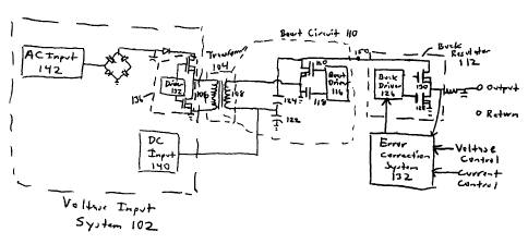
Fig. 2 illustrates a programmable power converter according to an embodiment
of the
present invention. The power converter may include a voltage input subsystem
102, a
transformer 104 including primary winding 106 and a secondary winding 108, a
boost circuit
110 that utilizes the secondary winding 108 as a boost inductor, a buck
regulator 112, and an
error correction system 132. The boost circuit 110 may also include a boost
driving device 116,
a first capacitor 122, a second capacitor 124, a first switching device 118,
and a second switching
device 120. The buck circuit 112 may include a buck driving device 126, a
third switch 128, and
a fourth switch 130.
The input voltage system 102 may receive a plurality of input voltages. In an
embodiment of the invention, one of the plurality of input voltages may be
input from an AC
input source 142. In an embodiment of the invention, one of the plurality of
inputs voltages may
be from a DC input source 140. In an alternative embodiment of the invention,
the input voltage
subsystem 102 may include an AC input source 142 and a DC input source 140.
s
20450561v2
CA 02471685 2004-06-18
i..,
If AC input source 142 is one of the plurality of input voltages, a bridge
rectifier 134
receives the AC voltage and outputs a DC voltage. A switching device 136
receives the DC
voltage and outputs a switched voltage. In an embodiment of the invention, the
switching device
136 may include a pair of switches, as illustrated in Fig. 2. In an embodiment
of the invention,
the switching device 136 may include one switch or a plurality of switches,
i.e., more than two.
The transformer 104 may receive the switched valtage at the primary winding
106. Depending
on the number of turns in the primary winding 106 in comparison to the number
of turns in the
secondary winding l 08, i.e., the primary-to-secondary turn ratio, the
switched voltage may be
increased or decreased to create an intermediate voltage. The intermediate
voltage may be
output from the secondary winding 108. Illustratively, the switched voltage
may be a
squarewave having a magnitude of.300 volts peak-to-peak value or having a
magnitude of 150
volts root mean squared (RMS). For example, if the primary-to-secondary turn
ratio is 10:1 and
the altenzating input voltage may measure 150 volts RMS, the intermediate
voltage may have a
magnitude of 15 volts RMS.
1 S A boost circuit 110 may be coupled to the transformer 104, specifically
the secondary
winding 108 of the transformer 104. The boost circuit 110 may utilize the
secondary winding
108 of the transformer as the boost inductor for the boost circuit 110. The
boost circuit 110 may
receive the intermediate voltage, modify the value of the intermediate
voltage, and output a
transformed voltage that is present at node 1 S0. The magnitude of the
transformed voltage that
is output by the boost circuit I 10 may be determined by a duty cycle of the
first switch 118 and a
duty cycle of the second switch 120 of the boost circuit 110. The duty cycle
of the first switch
118 and the duty cycle of the second switch I20 may be controlled by the boost
driving device
116. For example, if the duty cycle of the switches 118 and 120 of the boost
circuit 110 is 50~/0,
9
20450561v2
CA 02471685 2004-06-18
,..
then the magnitude of the transformed voltage may be boosted by a factor of
two from the
intermediate voltage. In an embodiment of the invention, the duty cycle of the
first switch 118
and the second switch 120 in the boost circuit 110 is fixed. For example, a RC
circuit may
determine the duty cycle of the first switch 118 and the second switch 120.
Under alternative
operating conditions, the duty cycle of the first switch 118 and the second
switch 120 in the
boost circuit 110 may be variable. In an embodiment, a signal or signals from
an error correction
subsystem 132 may assist in determining the duty cycle of the first switch 118
and the second
switch 120 in the boost circuit 110. Illustratively, a pulse width modulator
may receive a signal
from the regulator along with a second signal from an oscillating device and
may output a signal
to the boost driving device 116 of the boost circuit 110
If a DC input source 140 is one of the plurality of input voltages, the boost
circuit 110
may receive the input voltage from the DC input source 140. Illustratively,
the DC input voltage
may be supplied, for example, from a battery, a car, a train, or an airplane.
The boost circuit 110
may increase the value of the DC input voltage and may output a transformed
voltage. The boost
circuit 110 may utilize the secondary winding 108 as the boost inductor for
the boost circuit 110.
As discussed above, the magnitude of the transformed voltage present at node
150 in comparison
to the DC input voltage may be controlled by the duty cycle of the switches
118 and 120 in the
boost circuit 110. Illustratively, if the duty cycle of the switches 118 and
120 is 50%, then the
magnitude of the transformed voltage may be twice the magnitude of the DC
input voltage.
The buck regulator 112 may receive the boosted voltage from the boost circuit
110. The
buck regulator 112 may modify the magnitude of the transformed voltage to
create a regulated
voltage. The buck regulator I 12 may output the regulated voltage as the
output voltage at the
output terminal and may also a deliver an output current to the output
terminal. The duty cycle
io
Zo4sos6m2
CA 02471685 2004-06-18
w
of the third switching device 128 and the fourth switching device 130 in the
buck regulator 112
may control the magnitude of the regulated voltage. The third switching device
may be referred
to a pass switch I30 and the fourth switching device may be referred to as a
shunt switch 128.
For example, if the duty cycle of a pass switch 130 in the buck circuit 112 is
approximately equal
to 0.70, the magnitude of the regulated voltage may be equal to approximately
0.70 multiplied by
the transformed voltage. The duty cycle of the b~k regulator 112 may be
determined by the
buck driving device 126. The buck driving device I26 may be set to a fixed
duty cycle, e.g.,
50% duty cycle. Alternatively, the buck driving device 126 may be set to a
variable duty cycle
in the same manner as discussed above.
An error correction system 132 may regulate the external output voltage by
comparing it
to a reference voltage. Under certain operating conditions, the error
correction system 132 may
receive the regulated voltage and may compare it to a reference voltage. For
example, if the
portable appliance requires 24 volts DC, then a reference voltage may be
established to regulate
the regulated voltage. If the regulated voltage is not within an acceptable
range of the reference
voltage, then the error correction subsystem may transnut a voltage correction
signal to the buck
regulator 112 to adjust the duty cycles of the pass switch 130 and the shunt
switch 128. For
example, if the output voltage is 20 volts, the portable appliance requires 25
volts, only the buck
regulator 1 I2 is regulating the output voltage, and the duty cycle of the
pass switch 130 is 0.70,
then the correction signal to the buck regulator 112 rnay set the duty cycle
of the pass switch 130
to be increased to approximately 0.85 in order to drive the regulated voltage
to the required 25
volts.
In an embodiment of the invention, the modification signal may also be input
to the
driving device 116 of boost circuit 110 to modify the duty cycle of the first
switch 118 and the
m
Zo4sos6m2
CA 02471685 2004-06-18
second switch 120. The modification of the duty cycle of the switching device
in the boost
circuit 110 may increase or decrease the transformed voltage input to the buck
circuit 110.
In an embodiment of the invention, the error correction system 132 may
regulate the
output signals, i.e., the output current and the output voltage. The error
correction system 132
may regulate one of the regulated signals by verifying that the one of the
regulated signals
maintain a regulated signal to programming signal ratio. If the regulated
signal to programming
signal ratio is not within an acceptable range, the error correction system
132 may transmit a
correction signal to the buck regulator 112 to regulate the regulated signal
within the acceptable
range of the regulated signal to programming signal ratio. Illustratively, the
error correction
system 132 may regulate the regulated voltage and verify that the regulated
voltage to
programming voltage ratio is within an acceptable range. If the regulated
voltage is not within
the acceptable range, the error correction system 132 may transmit a voltage
correction signal to
the buck regulator 112 to modify the regulated voltage to be within the
acceptable range of the
regulated voltage to programming voltage ratio.
Fig. 3 illustrates a second embodiment of a voltage converter according to an
embodiment of the invention. The voltage converter includes an input voltage
system 201, a
transformer 203, a control circuit 220, at least two switching devices 208 and
210, and at least at
least two diodes 212 and 214. The voltage converter may also include a first
capacitor 216 and a
second capacitor 2I 8. In an embodiment of the invention, the voltage
converter may include a
buck regulator 226 and an error correction subsystem 232.
The input voltage system 201 may receive a plurality of input voltages. If an
AC input
source is one of the plurality of input voltages, a switched voltage is output
from the AC input
source through the bridge rectifier to the transformer 204 in the same manner
as discussed above
12
20450561Y1
CA 02471685 2004-06-18
regarding Fig. 2. In an embodiment of the invention, the switched voltage may
be a squarewave.
The transformer 202 outputs a transformed voltage across the seconding winding
230. The
magnitude of the transformed voltage is the magnitude of the switched voltage
multiplied by the
number of total turns of the secondary winding divided by the number of turns
of the primary
winding. For example, if the primary to secondary turns ratio is 15:1, i.e.,
the secondary-to-
primary toms ratio is 1:5, and the switched voltage is equal to 150 volts RMS,
the transformed
voltage is equal to 30 volts RMS. A rectifying circuit may be formed by the
first diode 212 and
the second diode 214. The rectifying circuit may receive the transformed
voltage, rectify the
transformed voltage, and output a DC voltage. Illustratively, if the
transformed voltage is 30
volts ItMS and is a squarewave, then the DC voltage is 30 volts.
The buck regulator 226 may receive the DC voltage, modify the DC voltage, and
output a
regulated voltage. The buck regulator 226 may output the regulated voltage as
the output voltage.
The buck regulator 226 may also output a regulated current as an output
current. The output
voltage and the output current is provided to the output terminal of the
voltage converter. An
ermr correction system 232 may receive the regulated signals, i.e., the
regulated voltage and the
regulated current. The error correction system 232 may transmit a correction
signal to the buck
regulator 226 to regulate the regulated signals in a similar manner as
described above regarding
Fig. 2. The error correction system 232 may regulate the regulated signals by
comparing the
regulated signals to programming signals and ensuring the regulated signal to
programming
signal ratio is within an acceptable range.
If a DC input source 203 is one of the plurality of input voltages provided by
the input
voltage subsystem 201, the DC input source 203 is coupled to a node 217
defined by the junction
of a first capacitor 216 and a second capacitor 218. The DC input source 203
is also coupled to a
13
2045Q561v2
CA 02471685 2004-06-18
. ..
v.
center tap of the secondary winding 230 of the transformer. This secondary
winding 230 of the
transformer is configured as an autotransfonner. In other words, the secondary
winding 230 of
the transformer is divided into a first autowinding 204 and a second
autowinding 206. In an
embodiment of the invention, the number of turns of the first autowinding 204
may be equal to
the number of toms of the second autowindiag 206. In an embodiment of the
invention, the
number of toms of the second autowinding 204 may not be equal to the number of
turns of the
second autowinding 206. A terminal of the first autowinding is coupled to the
drain of a first
switching device 208 and to an anode of a diode 214. A source of the first
switching device 208
is coupl~l to a reference ground. A gate of the first switching device 208 is
coupled to a control
circuit 220. A terminal of the second autowinding 206 is couplod to the drain
of the second
switching device 210 and the anode of the diode 212. A drain of the second
switch 210 is
coupled to a node 215 defined by the junction of the terminal of the second
autowinding 206 and
an anode of the diode 212. A source of the second switching device 210 is
coupled to ground.
The gaze of the second switching device 210 is coupled to the control circuit.
A node 240 is
defined as the junction of the cathode of the diode 214, second diode 212, and
the second
capacitor 218.
The control circuit 220 is driven at the same frequency as the driver of the
switching
device in the input system 201. The control circuit 220 drives the turning on
and off of the
switches 208 and 210. If the first switch 208 is conducting, i.e., turned on,
then the first tenminal
of the autowinding 204 is coupled to ground through the first switch. In other
words the first
terminal of the autowinding is coupled to 0 volts. The DC input voltage is
coupled to the center
tap 207 of the autotransformer. Thus, the DC input voltage is impressed across
the first
autowinding 204. In an embodiment of the invention, the second autowinding 206
may have the
14
20450561v2
CA 02471685 2004-06-18
J.
same number of turns as the first autowinding 204. Thus, the voltage across
the second
autowinding 206 may be the same as the voltage across the first autowinding
204. In other
words, the DC input voltage is impressed across the second autowinding 206.
Thus, at a second
terminal of the second autowinding 206, the transformed voltage is double the
DC input voltage.
This allows the charging of the second capacitor 218 to DC input voltage.
The operation of switch 210 is symmetrical to the operation of switch 208. In
a similar
fashion, when switch 2I0 is conducting, the second terminal of the second
autowinding 206 is
coupled to ground, the center tap 207 is coupled to DC input voltage, and the
first terminal of the
second sutowinding 204 is coupled to double the DC input voltage, if the
number of turns of the
first autowinding 204 is the same as the number of turns of the second
autowinding 206. Thin,
the voltages are just reversed from when switch 208 is conducting. Thus, when
switch 210 is
conducting, the second capacitor 218 is also charged to DC input voltage.
The combination of the activation of the switches 208 and 210 produce a
squarewave that
has a peak-to-peak voltage of two multiplied by the DC input voltage and an
RMS value of two
multiplied by the DC input voltage. The rectifying circuit, formed by the
diodes 212 and 214,
rectifies the squarewave to produce a DC voltage having a magnitude of two
multiplied by the
DC input voltage.
Similarly, the DC voltage at the node 240 is equal to double the DC input
voltage.
The DC voltage is then provided to the buck regulator 226. The operation of
the buck
regulator 226 is described in detail above. Similarly, the error correction
system may regulate
the regulated signals, i.e., the regulated voltage and the regulated current,
generated by the buck
regulator by maintaining the regulated signal to programming signal ratios.
The operation of the
error correction system is described in detail above.
20450561v2
CA 02471685 2004-06-18
Figs. 4(a), 4(b), 4(c), and 4(d) illustrate a schematic of the power converter
with an AC
input source and a DC input source according to as embodiment of the present
invention. Fig.
4(a) illustrates a voltage input system including an AC input source, a noise
cancellation circuit ,
and a triac-enabled doubling circuit according to an embodiment of the present
invention. The
voltage input system 402 includes an AC input source 404, a bridge rectifier
405, a noise
cancellation circuit 406, a triac-enabled multiplying circuit 408, and a
switching device 410. The
AC input source 404 provides an AC input to the bridge rectifier 405. The
bridge rectifier 405
outputs a rectified voltage. Depending on the magnitude of the AC input
voltage, the rectified
voltage may be multiplied by the triac-enable multiplying circuit 408 to
create a multiplied
voltage. The rectified voltage or the multiplied voltage may be input to the
switching device 410.
The switching device 410 may output a switched voltage. In an embodiment of
the present
invention, the switched voltage may be a squarewave. Illustratively, under
certain operating
conditions, the squarewave may have a peak-to-peak voltage magnitude of 300
volts and an
ItMS voltage magnitude of 150 volts. Common mode noise generated by the
switching device
4I0 may be cancelled out by a common mode cancellation waveform generated by
the noise
cancellation circuit 406. The noise cancellation circuit 406 and the triac-
enabled multiplying
circuit 408 are discussed in co-pending patent application entitled, "Common
Mode Noise
Cancellation Circuit," U.S, application serial number 10/452,162, filed May
30, 2003, which is
incorporated by reference.
The switched voltage may be output to the transformer 412, which includes a
primary
winding 414 and a secondary winding 416 (see Fig. 4(b)). The transformer 412
may receive the
switched voltage and may output an intermediate voltage across the entire
secondary winding
416. The magnitude of the intermediate voltage across the secondary winding
416 may be
16
20450561v2
CA 02471685 2004-06-18
determined by multiplying a magnitude of the switched voltage times the
secondary-to-primary
turns ratio. In other words, the number of turns of the secondary winding 41 b
divided by the
number of turns of the primary winding 414 (see Fig. 4(a)) is then multiplied
by the magnitude
of the switched voltage to determine the magnitude of the intermediate
voltage. Illustratively, as
shown in Fig. 4(a), the number of turns of the primary winding 414 is 20 and
the number of turns
of the secondary winding 416 is 4, which equals 1/5, i.e., 4 / 20. If the
magnitude of the
switched voltage is 150 volts 1ZMS, then in this illustrated embodiment, the
magnitude of the
intermediate voltage is 30 volts luviS.
Fig. 4(b) illustrates the rectifying circuit and the switching devices of the
power converter
according to an embodiment of the present invention. The intermediate voltage
is input to a
rectifying circuit 424. The rectifying circuit 424 may include switching
devices 420 and 422.
Switching devices 420 and 422 perform rectification on the
intenmediate/transformed voltage
and output a DC voltage to Vm;d 426. In an embodiment of the invention
illustrated in Fig. 4(b),
if the transformed voltage is a squarewave and has a magnitude of 30 volts
ltMS, the DC voltage
after rectification by the rectifying circuit 424 may be 30 volts DC.
The control circuit 434 transmits driving signals, Labeled DrvA and DrvB, to
the
switching devices 420 and 422, respectively. The driving signals lhvA and DrvB
are generated
by control subcircuits 436 and 438, respectively. Control subcircuit 436
compares an oscillating
signal, labeled OSC, with a reference voltage, e.g., 5 volts, to generate the
driving signal DrvA.
Similarly, control subcircuit 438 compares an oscillating signal, labeled OSC,
with a reference
voltage to generate signal DrvB. The driving signals DrvA and DrvB are never
active, e.g., they
are high at the same time because the inputs for the control subcircuit 438
are opposite to the
input for the control subcircuit 436. In other words, in control subcircuit 43
8, the reference
17
zo4sos6mx
CA 02471685 2004-06-18
1
voltage is input into the inverting input and the oscillating signal is input
into the non-inverting
input. In control subcircuit 436, the reference voltage is input into the non-
inverting input and
the oscillating signal is input into the inverting input. The generation of
the oscillating signal is
discussed below. In an embodiment of the invention, the duty cycle of driving
signals DrvB and
DrvA is 50~/0.
Fig. 4(c) illustrates a voltage input system including a DC input source and a
buck
regulator according to an embodiment of the present invention. A DC voltage is
input via
terminals 1 and 2 440. Comparator U 107-B 441 senses that DC voltage is
present within the
device. Q111 442 is a blocking device that prevents current from traveling
towards the DC input
IO source 440. The DC input voltage from the DC input source 440 is
represented by VDC;" 444 in
Fig. 4(c).
First reference voltage circuit 446 generates the reference voltage V~ which
is utilized in
other parts of the power converter. The first reference voltage circuit 446 is
coupled to VDC;
444. In an embodiment of the invention, the first reference voltage circuit
446 may limit V,~ to a
maximum of 16.2 volts. The limiting of the V~ is necessary since integrated
circuits utilized in
the power converter prefer not to receive input voltages greater than 20
volts.
Second reference voltage circuit 448 generates a plurality of reference
voltages for use in
other parts of the power converter. For example, in the embodiment of the
invention illustrated
in Fig. 4(c), a reference voltage of 5.1 volts, a reference voltage of 2.5
volts, and a reference
voltage of +5 volts are provided by the second reference voltage circuit 448.
The second
reference voltage circuit 448 is also coupled to VDC;" 444.
Refenzng back to Fig. 4(b), VDCin 444 is coupled to a terminal of a transistor
in
switching device 430. VDCin 444 is also coupled to a terminal of a transistor
in switching
18
10150561x2
CA 02471685 2004-06-18
device 432. VDC;" 444 is also coupled to the center node 458 of a capacitor
bank. The capacitor
bank is formed by the pair of capacitors 454 and the pair of capacitors 456.
Switching device
430 and switching device 432 are driven by control circuit 434. In the
embodiment of the
invention illustrated in Fig. 4(b), first control subcircuit 438 drives
switching device 430 via the
S drive signal DrvB and second control subcircuit 436 drives switching device
432 via the drive
signal DrvA. In an embodiment of the invention, a duty cycle of drive signal
DrvB is 50% and a
duty cycle of drive signal DrvA is 50%. Because switching device 420 and
switching device 432
utilize drive signal DrvA, both switching devices 420 and 432 may be fumed on
at the same time.
Similarly, because switching device 422 and switching device 430 both utilize
drive signal DrvB,
both of switching devices 422 and 430 may be turned on at the same time.
Switching device 430 corresponds to switching device 208 in Fig. 3 and
switching device
432 corresponds to switching device 210 in Fig. 3. Switching device 420
corresponds to diode
214 in Fig. 3 and switching device 422 corresponds to diode 212 in Fig. 3. The
operation of the
autotransformer, the control circuit 434, the switching devices 430 and 432,
and the rectifying
circuit 424 is similar to the operation described above regarding Fig. 3. The
secondary winding
416 of the transformer is configured as an sutotransformer. In other words,
the secondary
winding 416 of the transformer 414 has a first autowinding 4S0 and a second
autowinding 452.
In the embodiment of the invention illustrated in Fig. 4(b), the first
autowinding 450 and the
second autowinding 452 have an equivalent number of toms. In an embodiment of
the present
invention, the first autowinding 450 and the second autowinding 452 may not
have as equivalent
number of turns.
The drain of the switching device 430 is coupled to a terminal 451 of the
first
autowinding 450. The drain of the switching device 432 is coupled to nods 460.
VDC;" 444 is
19
2M50561v2
CA 02471685 2004-06-18
coupled to the center of the capacitor bank, e.g., 458. Node 458 is formed by
~e.lun~on of the
positive terminals of the pair of capacitors C I6 and C I 7 456 and the
negativc finals of the
pair of capacitors C 14 and C 15 454.
As the first control subcircuit 438 drives the first switching device 430 on,
terminal 451
of the first autowinding 450 is coupled to ground. YDC;~ 444 is coupled to ~e
center tap 453.
The coupling of VDC;~ to the center tap 453 places VDC;~ across the first
autowinding 450 for
the timeframe of the first switching device is closed on. Because the first
autowinding 450 and
the second autowinding 452 are an autotransfonner, the voltage across the
first autowinding 450
is also placed across the second autowinding 452, subject to reduction,
staying ~e one, or
increasing due to the first autowinding to the second autowinding turns ratio.
In the embodiment
of the invention illustrated in Fig. 4(b), the number of turns of the first
auto~nding 450 is equal
to the number of turns of the s~ond autowinding 452. Thus, VDC;" 444 maY be
placed across
the second autowinding 452. Thus, a transformed voltage having a magnitude of
2 x VDC;~ is
placed across the entire secondary winding in the timefrarne that the
switching device 430 is on.
I5 As discussed above, as the second control subcircuit 436 drives switching
device 432, a
similar process occurs. Terminal 455 of the second autowinding is coupled ~
ground, the center
tap 453 is still coupled to VDC;~, and terminal 451 is coupled to 2 x VDC;n~
Th~~ a voltage
having a magnitude 2 x VDCm is placed across the entire secondary windixzg
4I6. Thus, a
transformed voltage having a magnitude of 2 x VDC;" is placed across the
entire secondary
winding in the timeframe the switching device 432 is on.
Accordingly, in the embodiment of the invention illustrated in Fig. 4(b), ~e
transformed
voltage takes the form of a squarewave having a peak-to-peak voltage of Z x
VDC;~ and a RMS
voltage of 2 X VDC;".
Zo45es61.~
CA 02471685 2004-06-18
The rectifying circuit 424 may receive the transformed waveform and rectify
the
transformed waveform. Switching devices 420 and 422 may rectify the
transformed voltage. In
the embodiment of the invention illustrated in Fig. 4(b), the transformed
voltage has a magnitude
of 2 x VDC;" RMS. In the embodiment illustrated in Fig. 4(b), the transformed
voltage is a
squarewave. The rectification of a squarewave produces a DC value that is the
same as the value
of the RMS voltage. Thus, in the embodiment of the invention illustrated in
Fig. 4(b), the
rectified voltage has a magnitude of 2 x VDC;~ which is supplied to Vm;d 426.
Thus, 2 x VDC;
is present at node 460 and at V,~;d 426.
The driving signals output by the control circuit 434 are created by a first
control
subcircuit 438, driving signal DrvA, and a second control subcircuit 436,
driving signal DrvB.
The first control subcircuit 438 compares an oscillating waveform generated by
a waveform
generator 449 (see Fig. 4(c)) to a reference voltage, e.g., 5 volts, and
outputs DrvB to the
switching device 430 and the switching device 422. This means that the first
switching device
430 and the switching device 422 are turned on at the same time.
Illustratively, DrvB may be a
squarewave. Similarly, the second control subcircuit 436 compares the
oscillating waveform
generated by the waveform generator to a reference voltage, e.g., 5 volts and
outputs a DrvA to
the switching device 432 and the switching device 420. Illustratively, DrvA
may be a
squarewave. The second driving signal may be opposite in phase to the first
driving signal
because the inputs to the comparator U3-C pins 8 and 9 in the second control
subcircuit 436 are
opposite to the inputs to the comparator U3-C pins 6 and 7 in the first
control subcircuit 438. In
other words, DrvB may not activate switching devices 430 and 422 at the same
time as DrA
activates switching devices 432 and 420.
21
zoasossmz
CA 02471685 2004-06-18
..,.... , l
Fig. 4(c) illustrates the waveform generator and the buck regulator according
to an
embodiment of the present invention. The voltage at Vm;d 426 (see Fig. 4(b))
is input to the buck
regulator 470. The buck regulator 470 includes a first switch Q 102 472, e.g.,
a pass switch, a
second switch Q104 474, e.g., a shunt switch, a driving device U106 476, a
first comparator
U103-C 478, and a second comparator U103-D 480. When the buck regulator 470
turns on the
first switch Q102 472, the DC voltage at V~,;d is passed through to node 480.
When the buck
regulator toms on the second switch Q 102 474, the DC voltage at Vmid does not
pass through
and is instead shunted to ground. The voltage present at node 480 is a
regulated output voltage.
The voltage at node 480 is passed through to the output terminal 2 490 (see
Fig. 4(d)). A
regulated current is also transferred to output terminal 2 490.
Fig. 4(d) illustrates an error correction system in a power converter
schematic according
to an embodiment of the present invention. The buck regulator 470 (see Fig.
4(c)) may receive a
correction signal from the error correction system 500. The error correction
system S00 may
output a correction signal if a regulated signal to programming signal ratio
is not within an
acceptable range. The error correction signal is output at node 510.
Illustratively, the error
correction signal may be a voltage correction signal. The error correction
signal may also be a
current correction signal.
Node 510 is coupled to the non-inverting inputs of the comparator U 103-C and
U 103-D.
Thus, the correction signal is input to the non-inverting inputs of the
comparators U103-C and
U 103-D. The waveform generator 449 (see Fig. 4(c)) also inputs an oscillating
waveform into
the inverting terminals of the comparators U103-C 478 and U103-D 480 (see Fig.
4(c)). The
comparators U103-C 478 and U103-D 480 compare the oscillating waveforrn to the
correction
signal and output a pass switch driving signal and a shunt switch driving
signal based on the
22
20450561v2
CA 02471685 2004-06-18
comparison. The comparators U103-C 478 and U103-D 480 input a pass switch
driving signal
and a shunt switch driving signal to the driving device 476 (see Fig. 4(c)).
The driving device
U 106 476 transmits a pass switch signal to the pass switch 472 (see Fig.
4(c)) and a shunt switch
driving signal to the shunt switch 474 (see Fig. 4(c)). The pass switch signal
and the shunt
S switch signal may never be active at the same time. The resistors 8113,
8114, and Rl 15 (see
Fig. 4(d)) are utilized to place a delay in between the tunung on of the pass
switch 472 and the
tuniing on of the shunt switch 474.
If no voltage regulation is required, meaning the error correction signal is
not active or
the correction signal is not transmitted from the error correction system 500,
the duty cycle of the
pass switch 472 (see Fig. 4(c)) may be maintained at its current level.
Maintaining the duty
cycle of the pass switch 472 results in the regulated voltage and the output
voltage maintaining
existing values. If a con ection signal is output from the error correction
system 500 and it is a
voltage correction signal, the duty cycle of the pass switch 472 may be
increased or decreased.
Illustratively, if the duty cycle of the pass switch 472 is increased, then
the regulated voltage and
output voltage may be increased. Alternatively, if the duty cycle of the pass
switch 472 is
decreased, then the output voltage may be decreased.
If an error correction signal is output from the error correction system 500
and it is a
current correction signal, the duty cycle of the pass switch 472 (see Fig.
4(c)) may be decreased
in order to lower the output voltage and hence the regulated current.
The current correction subsystem 520 may generate a current correction signal.
A
programming current signal may be input to pin 12 of U104-B. The magnitude of
the
programming current is dependent upon the value of a resistor, which may be
located in a cable
or a connector coupled to the power converter. A reference current may be
input to pin 13 of
23
20450561v2
CA 02471685 2004-06-18
l
U104-B. The reference current may be generated by utilizing a voltage to
current converter such
as U 104-C and the associated circuitry. The reference current input to U 104-
C has a linear
relationship to the regulated current, i.e., the output current. If the ratio
of the reference current
to programming current is not within an acceptable range, the current
correction subsystem 520
generates a current correction signal to node S I 0. Also, because the
reference current has a
linear relationship to the regulated current, it follows that the ratio of the
regulated current to
programming current is not within an acceptable range, the current correction
subsystem 520
generates a current correction signal to node 510.
The voltage correction subsystem 530 may generate a voltage correction signal.
A
programming voltage may be input to pin 3 of U104-A. A reference voltage may
be generated
from the regulated voltage and may have a linear relationship to the regulated
voltage. The
reference voltage is input to pin 2 of U 104-A. If the ratio of the reference
voltage to the
progialnming voltage is not within an acceptable range, the voltage correction
subsystem 530
generates a voltage correction signal to node 510. Because the reference
voltage has a linear
relationship to the reference voltage, it follows that if the regulated
voltage to programming
voltage ratio is not within an acceptable range, the voltage correction
subsystem 530 may
generate a voltage correction signal to node 510.
The soft start lockout detector 540 is illustrated in Fig. 4(d). The
overvoltage lockout
detector 542 identifies if DC input voltage is too high. The soft start system
544 ramps up the
voltage during the starting of the system in a controlled manner.
The converter may also output a reference voltage on pin S 492. U104-D
generates the
reference voltage. In the embodiment of the invention illustrated in Fig.
4(d), the reference
voltage has a value of +5 volts.
24
20450561v2
CA 02471685 2004-06-18
The waveform generator 449 (see Fig. 4(c)) may generate the oscillating signal
utilized
by the buck regulator 472 and the switching devices 420, 422, 430, and 432
(see Fig. 4(b)). The
waveform generator 449 generates an oscillating signal having a frequency that
is the same of
the frequency being output by driving device Ul of the switching device 410
(see Fig. 4(a)).
Driving device U1 of the switching device U1 generates the clocking frequency
upon startup of
the power converter and this frequency is transferred to the waveform
generator 449 through a
winding 447 off the transformer 412.
While the description above refers to particular embodiments of the present
invention, it
will be understood that many modifications may be made without departing from
the spirit
thereof. The accompanying claims are intended to cover such modifications as
would fall within
the true scope and spirit of the present invention. The presently disclosed
embodiments are
therefore to be considered in all respects as illustrative and not
restrictive, the scope of the
invention being indicated by the appended claims, rather than the foregoing
description, and all
changes which come within the meaning and range of equivalency of the claims
are therefore
intended to be embraced therein.
20450561~I