Note: Descriptions are shown in the official language in which they were submitted.
CA 02472012 2004-06-29
WO 03/061275 PCT/US02/40035
IMAGING DEVICE AND RELATED METHODS
Related Apulication
[0001] This application is based on prior copending provisional patent
application Ser. No.
60/347,391, filed on January 9, 2002, the benefit of the filing date of which
is hereby claimed
under 35 U.S.C. ~ 119(e).
Technical Field
[0002] This invention relates to imaging devices. More particularly, iii one
embodiment, the
invention is directed to a miniature imaging device and related methods.
Background of the Invention
[0003] Spectral analysis of living tissue can be used to detect various forms
of cancer and other
types of diseases. In spectral analysis, light illuminates a tissue region
under examination and a
light detector detects optical properties of the illuminated tissue region by
measuring light energy
modified by its interaction with the tissue region in a pre-determined
frequency and amplitude
domain. Optical properties include absorption, luminescence, fluorescence,
frequency and time
domain response to various materials injected to the tissue region and other
electromagnetic
responses. I?iseased tissue may be identified by comparing a spectrum obtained
to spectra of
normal tissue obtained under the same controlled conditions.
[0004] Traditional image sensors include a two dimensional array of photo-
detectors (pixels)
that are accessed individually by electronics on the same chip, or external to
the chip. A black
and white image is formed by digitizing the amplitude of each pixel, which
creates a gray scale.
Color images function in a similar manner, but employ complex algorithms to
compute the color.
One common color sensor has a color maslc that is placed on the image sensor.
The color maslc
is a light filter that allows only certain light wavelengths to penetrate and
reach the detector.
Then, by comparing amplitudes of adjacent pixels, the color is calculated.
[0005] One disadvantage of conventional image sensors is size due to the
number of pixels
(photo-detectors) required to produce a quality image. Another disadvantage of
conventional
image sensors is the complex electronics involved in addressing each pixel
(photo-detector).
CA 02472012 2004-06-29
WO 03/061275 PCT/US02/40035
Summary of the Invention
[0006] In one embodiment, the invention combines a scamling system similar to
a display-type
raster scan with a single photodiode to create an image. By doing so, the
invention provides an
imaging device that is smaller than traditional imaging devices.
[0007] According to one embodiment, the imaging device of the invention
includes a light
source unit, a photo-sensor and a scamling assembly. The light source unit is
fixedly moiulted in
the first end of an elongated sheath and is adapted for illuminating a target.
The photo-sensor is
mounted on the scanning assembly, also located in the first end of the
elongated sheath, and is
adapted to detect light energy from the target. The scanning assembly scans
the target to enable
the photo-sensor to detect light energy from each of a plurality of locations
on the target.
According to a further embodiment, the imaging device of the invention
synchronously digitizes
the output from the photo-sensor from each of the plurality of locations on
the target to generate
an image of the target. According to a further embodiment, the light source
unit provides wide
angle/divergent illumination. According to one embodiment, the light energy
includes reflected
light. According to another embodiment, the light energy contains fluorescent
light.
[0008] According to another embodiment, the scanning assembly includes a
platform movably
mounted on a constant velocity pivot joint adapted for enabling the scanning
assembly to scan
the target with a photo-sensor in two directions. According to one embodiment,
the scanning
assembly is adapted to scan the target at a sweep frequency of greater than or
equal to about
llcHz. According to a further embodiment, the scanning assembly is adapted to
scan a target at a
sweep frequency above about 5 lcHz. According to a further embodiment, the
scanning assembly
is adapted to scan a target at a sweep frequency above about 10 lcHz.
According to a further
embodiment, the scanning assembly is adapted to scan a target at a sweep
frequency above about
15 lcHz. According to another embodiment, the scanning assembly is adapted to
completely
scan the target at a scan frequency of greater than or equal to about 2 Hz.
According to a further
embodiment, the scanning assembly is adapted to completely scan a target at a
scan frequency
above about 'S Hz. According to a further embodiment, the scanning assembly is
adapted to
completely scan a target at a scan frequency above about 10 Hz. According to a
further
embodiment, the scanning assembly is adapted to completely scan a target at a
scan frequency
above about 20 Hz. According to a further embodiment, the scanning assembly is
adapted to
completely scan a target at a scan frequency above about 30 Hz. According to a
further
embodiment,( the scanning assembly is adapted to completely scan a target at a
scan frequency
above about 40 Hz. According to a further embodiment, the scanning assembly is
adapted to
CA 02472012 2004-06-29
WO 03/061275 PCT/US02/40035
-3-
completely scan a target at a scan frequency above about 50 Hz. However,
various sweep and
scan frequencies may be employed without deviating from the scope of the
invention.
According to a further embodiment, the scanning assembly includes
electromagnetic actuators
for controlling platform movement. According to an alternative embodiment, the
scanning
assembly includes piezoelectric actuators for controlling the platform
movement. According to
another alternative embodiment, the scanning assembly includes microelectronic
machine
(MEMS) actuators for controlling the platform movement.
[0009] According to one feature, the MEMS actuators are fabricated in silicon,
which is also a
common substrate material for both photo-sensors and lasers diodes. The photo-
sensor and/or
the laser diode may be fabricated directly on the MEMS actuator plate using
standard
semiconductor processing techniques. This reduces the need for bonding
discrete parts to the
scanning platform, with the advantage that it may reduce the overall mass of
the platform,
allowing for higher scan rates and lower drive power. According to a further
embodiment, the
photo-sensor is a single pixel photo-sensor.
[0010] According to one embodiment, the imaging device includes an aperture
oriented with
respect to the photo-sensor and adapted for limiting light energy from the
target from impinging
on the photo-sensor. According to one feature, the aperture allows
substantially only the light
energy from one target location at a time to impinge on the photo-sensor.
According to another
feature, the aperture includes a fixed focal length lens.
[0011] According to an alternative embodiment, the imaging device of the
invention includes a
light source unit, a photo-sensor and a scanning assembly, wherein both the
light source unit and
the photo-sensor are movably mounted on a scanning assembly in the first end
of an elongated
sheath. The light source illuminates the target as the scanning assembly scans
a plurality of
locations on the target. _ The photo-sensor synchronously captures the light
energy from each of
the scamled locations on the target. The imaging device of the invention then
synchronously
digitizes the output from the photo-sensor from each of the plurality of
locations on the target to
generate an image of the target.
[0012] According to another alternative embodiment, the imaging device of the
invention
includes a light source unit, a photo-sensor and a scanning assembly, wherein
the photo-sensor is
fixedly mounted on a platform in the first end of an elongated sheath and the
light source is
movably moiulted on a scanning assembly, also in the first end of the sheath.
According to one
feature of this embodiment, the scanning assembly scans the target to
discretely illuminate each
of a plurality locations on the target. According to a further feature, the
photo-sensor
CA 02472012 2004-06-29
WO 03/061275 PCT/US02/40035
-4-
synchronously captures the light energy from each of the illuminated
locations. According to
another feature the imaging device of the invention then digitizes the output
from the photo-
sensor from each location on the target to generate an image of the target.
[0013] According to one embodiment, the light source employs one or more LEDs.
According
to another embodiment, the light source employs one or more laser diodes. In a
further
embodiment, the light source unit employs a fixed focal length lens to focus
the light onto
discrete locations of the target. According to a further embodiment, the photo-
sensor employs a
wide angle lens to capture light energy from each of the scanned locations on
the target.
[0014] According to a further embodiment, the first end of the elongated
sheath forms a lens
adapted for focussing the light from the light source on to each of the
scanned locations on the
target. According to another embodiment, the first end of the elongated sheath
forms a lens
adapted for focussing light energy from each of the scanned locations on the
target back on to the
photo-sensor.
[0015] According another alternative embodiment, the invention provides a
scanning system
having a light source and a photo-sensor, both located discretely from a first
end of an elongated
sheath to illuminate a location on a target. A beam splitter/combiner couples
light from the light
source through a fiber optic connection to an end of the fiber optic
connection located in the first
end of the elongated sheath. The beam splitter/combiner also couples light
energy from the
target through the first end of the elongated sheath and the same fiber optic
connection to the
photo-sensor. According to a further embodiment, the scanning system includes
a scanning
mechanism, located in the first end of the elongated sheath and adapted for
moving the end of
the fiber optic connection to scan synchronously light from the source onto
each of a plurality of
locations on the target, and to transfer light energy from each of the
plurality of locations on the
target back to the photo-sensor. According to a further feature, the scanning
system of the
invention synchronously digitizes the output from the photo-sensor due to each
of the plurality of
scanned locations on the target to generate an image of the target.
[0016] According to another embodiment, the invention provides a scanning
system adapted for
generating color images of a target. According to one embodiment, the scanning
system of the
invention employs field sequenced color (e.g., red, blue, green) LEDs pulsed
in sequence for
each of the plurality of locations illuminated on the target to achieve a
color image of the target.
According to one preferred embodiment, the imaging devices and methods of the
invention axe
particularly adapted for analysis of living tissue.
CA 02472012 2004-06-29
WO 03/061275 PCT/US02/40035
-5-
Brief Description of the Drawings
[0017] The patent or application file contains at least one drawing executed
in color. Copies of
this patent or patent application publication with color drawings will be
provided by the Office
upon request and payment of the necessary fee.
[0018] The foregoing and other objects of the invention and the various
features thereof may be
more fully understood from the following description when read together with
the accompanying
drawings in which lilce reference designations generally refer to the same or
similar parts
throughout the different views and in which the depicted components are not
necessarily drawn
to scale.
[0019] Figure lA is a schematic diagram depicting an imaging device employing
a scanned
detector, according to an illustrative embodiment of the invention;
[0020] Figure 1B is a schematic side view of an imaging device employing a
fixed position light
source and a sca~med detector, according to an illustrative embodiment of the
invention;
[0021] Figure 1 C is a schematic top view of the imaging device of Figure 1 B;
[0022] Figure 2A is a schematic side view of an imaging device, employing a
scanned light
source and a scanned detector, according to an illustrative embodiment of the
invention;
[0023] Figure 2B is a schematic top view of the imaging device of Figure 2A;
[0024] Figure 3 is a schematic side view of an imaging device employing a
scanned light source
and fixed position detector, according to an illustrative embodiment of the
invention;
[0025] Figure 4 is a schematic diagram depicting an imaging device employing a
scanning
device located remotely from a light source and a detector, according to
another illustrative
embodiment of the invention;
[0026] Figure 5 depicts a pattern for a circular type of image scan, according
to an illustrative
embodiment of the invention;
[0027] Figure 6 depicts a pattern for a spiral type of image scan, according
to an alternative
illustrative embodiment of the invention;
[0028] Figure 7A depicts an image pattern used as a test pattern, according to
an illustrative
embodiment of the invention;
[0029] Figure 7B depicts the image pattern of Figure 7A as the image is seen
by a single pixel
scanning camera, according to an illustrative embodiment of the invention;
[0030] Figure 7C depicts the image pattern of Figure 7B as an amplitude color
map, according to
an illustrative embodiment of the invention;
[0031] Figure 8A is another illustrative scan of an image drawn on a piece of
paper; and
CA 02472012 2004-06-29
WO 03/061275 PCT/US02/40035
-6-
[0032] Figure 8B is a scan of the same image of Figure 8A with the addition of
a tab to show
orientation.
Description of an Illustrative Embodiment
[0033] As described in summary above, the invention, in one embodiment, is
directed to a
miniature imaging device. In one embodiment, the imaging device is located in
the tip of an
elongate sheath such as a catheter. The sheath may be inserted into a human
body to observe
images of target tissue. According to one embodiment, the imaging device of
the invention is
employed where conventional endoscopes are too large to be useful.
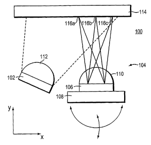
[0034] Figure lA is a schematic diagram depicting an imaging device 100
employing a scanned
detector, according to an illustrative embodiment of the invention. As
depicted, the imaging
device 100 includes a fixedly mounted light source 102 and a scanned photo-
sensor assembly
104. The scanned photo-sensor assembly 104 includes a photodiode 106 mounted
on a scanning
device 108 adapted to move along two axes (x,y). The imaging device 100 also
includes a wide
angle lens 112 mounted relative to the light source 102 and adapted to focus
light from the light
source 102 onto an entire target 114. The scanning device 108 synchronously
scans the
photodiode 106 to receive light energy from each of a plurality of locations,
such as the locations
116a-116c, on the target 114. A focussing lens 110, located relative to the
photodiode 106 limits
the light energy from the target from impinging on the photodiode 106. More
particularly, the
focussing lens 110 allows substantially only light from a particular one of
the plurality of
scanned target locations to impinge on the photodiode at any one time.
Subsequent to scanning
the entire target or a region of interest, the scanning device 100 digitizes
the outputs from the
photodiode 106 for synchronously captured images for each of the plurality of
scanned locations
on the target 114 to generate a high quality image of the target 114.
[0035] Figure 1B is a schematic side view of am imaging device 120 employing a
fixed position
light source and a scanned detector of the type illustrated in Figure lA.
Figure 1C is a schematic
top view of the imaging device of Figure 1B. Referring to Figures 1B and 1C,
the imaging
device 120 includes four light source assemblies 122, 123, 125 and 127; a
photo-sensor assembly
124, a platform 126; a base 128, a pivot 130; x-axis actuators 132a and 132b;
and y-axis
actuators 133a and 133b, all located in the end 134 of an elongated sheath
139. The light source
assemblies 122, 123, 125 and 127 are all fixedly mounted to a front face of
the base 128. Each
of the light source assemblies include an LED and a wide angle lens adapted
for illuminating the
target 136. More specifically, the light source assembly 122 includes an LED
122a and a wide
angle focussing lens 122b. Similarly, the light source assembly 123 includes
an LED 123a and a
CA 02472012 2004-06-29
WO 03/061275 PCT/US02/40035
_7-
wide angle focussing lens 123b; the light source assembly 125 includes an LED
and a wide angle
focussing lens; and the light source assembly 127 includes an LED and a wide
angle focussing
lens. Each LED is also powered by an LED power wire (e.g., 121a and 121b).
According to one
illustrative embodiment, the light source assemblies 122, 123, 125 and 127 may
illuminate the
target 136 with any frequency of light, either concurrently or in a sequenced
fashion. In one
illustrative example, the light source assemblies 122, 123, 125 and 127 may
illuminate the target
136 with white light for black and white image generation, and sequenced red,
green and blue
light, for color image generation. However, any other combination of
wavelengths may be
employed without deviating from the scope of the invention. In other
embodiments, for
pa~.-ticulax applications, such as scans that need to penetrate blood, the
light source assemblies
illtuninate the taxget 136 with infrared light. According to one feature of
the illustrated
embodiments, each of the light source assemblies are mounted at an angle
relative to the plane of
the platform 126. Although the embodiment of Figures 1B and 1C depict four
light source
assemblies, any number may be employed, limited by size and power constraints.
[0036] The photo-sensor assembly 124 fixedly mounts on a platform 126. The
platform 126, in
turn, movably mounts the base 128 by way of a universal pivot joint 130. The
universal pivot
joint 130 enables the platform 126 to move in both the x and y-axes. The
actuators 132a, 132b,
133a and 133b actuate the movement of the platform 126 with respect to the
base 128. More
particularly, the actuators 132a and 132b actuate the platform 126 along the x-
axis and the
actuators 133a and 133b actuate the platform 126 along the y-axis. In one
embodiment, the
actuators are processor controlled. According to one preferred embodiment, the
actuators are
electromagnetic. However, according to other embodiments, the actuators may be
MEMs or
piezoelectric actuators. Control signals are transmitted to the actuators
132a, 132b, 133a and
133b via scan control wires (e.g., 131a and 131b).
[0037] According to the illustrative embodiment, the actuators 132a, 132b,
133a and 133b
actuate the platform 126 in a predefined pattern (e.g., spiral, circle, raster
scan or the like) to scan
the target 136 to enable the photo-sensor assembly 124 to detect light energy
from each of a
plurality of locations on the target 136. The detected light may be, for
example, fluorescent or
reflected light and may be from anywhere in the spectrum, including visible
and infrared. In one
embodiment, the actuators 132a, 132b, 133a and 133b are pulsed to cause the
platform 126 to
move. In a further embodiment, the actuators are operated at resonance to
reduce the power
necessary to actuate the platform. According to the illustrative embodiment,
the photo-sensor
assembly 124 includes a photo-sensor 124a (preferably a single photo-diode)
and a focussing
CA 02472012 2004-06-29
WO 03/061275 PCT/US02/40035
_g_
lens and/or apeuture 124b. The focussing lens or aperture 124b limits the
amount of light energy
from the target allowed to impinge on the photo-sensor 124a. According to one
feature, the
lens/aperture 124b allows only the light energy from one target location at a
time to impinge on
the photo-sensor 124a. Optionally, the photo-sensor assembly 124 includes a
mask on the photo-
sensor 124a to fiu-ther narrow the field of view (i.e., the selectivity).
According to another
feature, the lens is a fixed focal length converging lens. In one embodiment,
the lens is a
gradient index lens. According to another feature, the end 134 of the
elongated sheath 139 forms
or includes a lens 140 for assisting in providing light from the source
assemblies to the target 136
and/or focussing light energy from the target 136 back to the photo-sensor
124a.
[0038] According to a further feature, the illustrative imaging device 120
synchronizes the
motion with the capture circuitry and digitizes the output from the photo-
sensor 124a for each of
the plurality of locations (e.g., 138) on the target 136 to generate an image
of the target 136.
[0039] According to one embodiment, the illustrative imaging device is about
one millimeter
square in size and provides about one hundred micron resolution.
[0040] Figures 2A and 2B depict an alternative embodiment 200 of the
invention, wherein both
the light source assemblies 122, 123, 125 and 127, and the photo-sensor
assembly 124 are
mounted on the platform 126 and can thus be directed at each of a plurality of
locations on the
target 136. Rather than the wide angle divergent lenses employed in the
embodiment of Figures
1B and 1C, according to the illustrative embodiment of Figures 2A and 2B, the
light source
assembly lenses (e.g., 122b and 123b) are fixed focal length lenses that focus
light from the light
source assemblies to each of the plurality of locations being scanned on the
target 136. Other
than this difference, the embodiment of Figures 2A and 2B operates in
essentially the same
fashion as the embodiment of Figures 1B and 1C.
[0041] Figure 3 is a schematic side view of an imaging device 300 employing a
scanned light
source and fixed position detector, according to an illustrative embodiment of
the invention.
According to the illustrative embodiment of Figure 3, the light source
assembly 122 is fixedly
mounted on the platfornl 126. As in the previous embodiments, the platform 126
is movably
mounted to the base 128.by way of the universal pivot 130 and actuated by the
x-axis actuators
132a and 132b and the y-axis actuators. The photo-sensor assembly 124 is
fixedly mounted on
the base 128 at a location adjacent to the platform 126. In this embodiment,
the light source
assembly 122 employs a fixed focal length lens 122b and the photo-sensor
assembly 124
employs a wide angle lens 124b.
CA 02472012 2004-06-29
WO 03/061275 PCT/US02/40035
-9-
[0042] According to the illustrative embodiment of Figure 3, the actuators
actuate the platform
126 along the x- and y-axes in a predefined pattern (e.g., spiral, circle,
raster scan or the lilce) to
scan the target 136 to enable the light source assembly 122 to illuminate
discretely each of a
plurality of locations on the target 136 with, for example, white light for
blaclc and white image
generation, or sequenced red, green and blue light, for color image
generation. Although only
one light source assembly is depicted in Figure 3 and as discussed above, any
number of light
source assemblies may be mounted on the platform 126 without deviating from
the scope of the
invention.
[0043] According to the embodiment of Figure 3, the photo-sensor assembly 124
includes a
photo-sensor 124a (preferably a single photo-diode) and a wide angle lens
124b. The lens allows
substantially all of the light energy from the target 136 resulting from the
light from the source
assembly 122 to impinge on the photo-sensor 124a. By synchronously scanning
the liglit source
discretely over each of a plurality of locations on the target 136 and
digitizing the output from
the photo-sensor 124a for each of the plurality of locations, the sensor
device of Figure 3
generates an image of the target 136.
[0044] Figure 4 depicts a photo-sensor system 400 according to an illustrative
embodiment of
the invention. The system 400 includes a light source 402 and a photo-sensor
404, both located
discretely from a first end 406 of an elongated sheath 408 to illuminate a
location on a target
136. A beam splitter/combiner 410 couples light from the light source 402
through a fiber optic
comzection 412 to an end 414 of the fiber optic connection 412 located in the
first end 406 of the
elongated sheath 408. The beam splitter/combiner 410 also couples light energy
from the target
136 through the first end 406 of the elongated sheath 408 and the fiber optic
connection 412 to
the photo-sensor 404. According to the illustrative embodiment of Figure 4,
the scanning system
400 includes a scanning mechanism 416, located in the first end 406 of the
elongated sheath 408,
and adapted for moving the end 414 of the fiber optic connection 412 to scan
synchronously
light from the source 402 onto each of a plurality of locations on the target
136, and to transfer
light energy from each of the plurality of locations on the target 136 back to
the photo-sensor
404. According to one illustrated feature, the system 400 is configured for
locating the light
source 402 and/or the photo-sensor 404 remotely from the elongated sheath 408.
According to a
further feature of the illustrative embodiment of Figure 4, the scanning
system 400
synchronously digitizes the output from the photo-sensor 404 due to each of
the plurality of
scanned locations on the target 136 to generate an image of the target 136.
CA 02472012 2004-06-29
WO 03/061275 PCT/US02/40035
-10-
[0045] Although the above embodiments describe scanning the target directly,
in alternative
embodiments, a lens, such as the lens 140, may be employed for image
reduction. Then, the
reduced image may be scanned. In this way, the necessary excursion of the
platform 126 and the
scan time can be reduced.
[0046] Figures 5 depicts a circular scanning pattern according to an
illustrative embodiment of
the invention. By starting in the center of the imaging area of the target,
the image is acquired by
moving the scanning device such that the scan produces a circular pattern with
increasing
diameter. The diameter increases until the end of the viewing area is reached.
The scanned spot
does not have to return to the center for the next frame. Instead, the
illustrative imaging device
of the invention acquires the data differently from that of the increasing
diameter circle. The
data is now acquired using a circular pattern with a decreasing diameter until
the center of the
imaging area is reached. In one embodiment, odd numbered frames use the
increasing diameter
scan, while even numbered frames use the decreasing diameter scan. The
scanning device of the
invention digitizes the information appropriately based on the phase of the
scan pattern (i.e.,
increasing or decreasing diameter). The acquired data is essentially in polar
coordinates (r,0).
The polar coordinates can be converted to Cartesian coordinates for image
reconstruction.
Figure 6 depicts a spiral scan pattern according to another illustrative
embodiment of the
invention. According to other illustrative embodiments, polygonal scanning
patterns, such as
square scanning patterns are employed. It should be noted that any scanning
pattern may be used
without deviating from the scope of the invention.
[0047] Figure 7A depicts an image that was scanned with an actual device
constructed in accord
with the principles of the invention. Figure 7B depicts the raw data in three-
dimensional
perspective corresponding to the image of Figure 7A and generated by an
illustrative
embodiment of the invention employing a single pixel photo-sensor. Figure 7C
is amplitude
color map corresponding to the image of Figure 7A and generated by an
illustrative embodiment
of the invention employing a single pixel photo-sensor. Figure 8A depicts
another example of a
scanned image generated by an illustrative embodiment of the invention. In
Figure 8A,
dimensions are shown on the x- and y-axes in millimeters. Figure 8B depicts
another example of
a scanned image, wherein the image includes a tab to show orientation. In
Figure 8B,
dimensions are shown along the x-axis in millimeters.
[0048] As can be seen from the above illustrative embodiments, the invention
provides a photo-
sensor device that is inexpensive to manufacture and smaller than the current
technology. In one
embodiment, the invention employs a single miniature detector as opposed to an
array of
CA 02472012 2004-06-29
WO 03/061275 PCT/US02/40035
-11-
detectors, or bundles of fibers. One problem solved by the invention is that
it can go into areas
of the human body that an endoscope cannot. Additionally, since the device of
the invention is
inexpensive to malce, it can be disposable. Additionally, the devices of the
illustrative
embodiments may be employed with any available display technology.
What is claimed is: