Note: Descriptions are shown in the official language in which they were submitted.
CA 02472029 2004-06-29
WO 03/045556
PCT/US02/38047
METHOD, APPARATUS AND ARTICLE FOR MICROFLUIDIC CONTROL VIA
ELECTROWETT1NG, FOR CHEMICAL, BIOCHEMICAL AND BIOLOGICAL
ASSAYS AND THE LIKE
BACKGROUND OF THE INVENTION
Field of the Invention
This disclosure is generally related to the manipulation of fluids,
for example, manipulating fluids for performing chemical, biochemical,
cellular
and/or biological assays, and more particularly to electrowetting to
manipulate
electrolytic fluids, for example reactants such as agents and reagents.
Description of the Related Art
Two of the primary factors currently driving the development of
microfluidic chips for pharmaceuticals, the applied life sciences, and medical
diagnostics include: (1) the reduction of sample volumes to conserve
expensive reagents and reduce disposal problems; and (2) the reduction of test
turnaround times to obtain laboratory results. Through the engineering of new
processes and devices, time-consuming preparatory procedures and protocols
can be automated and/or eliminated. This has been the motivation behind the
development of microfluidics associated with lab-on-a-chip systems, biochips,
and micro Total Analytical Systems ([1-FAS). The result has been a large
number of mechanical designs for pumps, valves, splitters, mixers, and
reactors
that have been micro-fabricated in channels using photolithographic and other
bonding and assembly methods.
There is also a growing need in the fields of chemistry,
biochemistry and biology for performing large scale, combinatorial testing.
One
type of large-scale combinatorial testing employs microarrays. Each microarray
consists of hundreds or thousands of spots of liquid applied to a slide or
"biochip." Each spot may, for example, contain a particular DNA segment. The
microarrays are created using robots which move pins to wick up the
appropriate fluid from reservoirs and to place each individual spot of fluid
precisely on the slide. The hardware is expensive and the slides are time
consuming to manufacture.
CA 02472029 2004-06-29
WO 03/045556
PCT/US02/38047
BRIEF SUMMARY OF THE INVENTION
Under one aspect, an active matrix microfluidic platform employs
thin film transistor active ("TFT") matrix liquid crystal display technology
to
manipulate small samples of fluid for chemical, biochemical, or biological
assays without moving parts, for example using a two-dimensional matrix array
of drive electrodes.
In another aspect, the active matrix microfluidic platform may
employ existing active matrix addressing schemes and/or commercial "off-the-
shelf" animation software to program assay protocols.
In a further aspect, a feedback subsystem determines an actual
location of a fluid in the microfluidic structure, and provides location
information
for display, for example on an active matrix display, and/or to control
movement
of one or more fluid bodies in the microfluidic structure.
The active matrix microfluidic platform may provide a low cost and
efficient method and apparatus for the pharmaceutical industries to perform
drug-screening applications. The active matrix microfluidic platform may also
provide a low cost and efficient method and apparatus for the chemical
industries to perform combinatorial chemistry applications. The active matrix
microfluidic platform may additionally provide a low cost and efficient method
and apparatus for the bioscience industries to perform gene expression
microarray research. The active matrix microfluidic platform may further
provide a low cost and efficient method and apparatus for clinical diagnostic
bioassay, as well as lead to additional "lab-on-a-chip" applications.
BRIEF DESCRIPTION OF THE SEVERAL VIEWS OF THE DRAWINGS
In the drawings, identical reference numbers identify similar
elements or acts. The sizes and relative positions of elements in the drawings
are not necessarily drawn to scale. For example, the shapes of various
elements and angles are not drawn to scale, and some of these elements are
arbitrarily enlarged and positioned to improve drawing legibility. Further,
the
particular shapes of the elements as drawn, are not intended to convey any
information regarding the actual shape of the particular elements, and have
been solely selected for ease of recognition in the drawings.
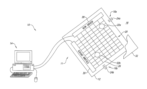
Figure 1 is a schematic diagram of a microfluidic control system,
including a controller in the form of a computing system, and a microfluidic
2
CA 02472029 2004-06-29
WO 03/045556
PCT/US02/38047
platform having a microfluidic structure including a two-dimensional matrix
array
of drive electrodes, row and column driving circuits and a ground electrode.
Figure 2 is a schematic diagram of the computing system and
microfluidic platform of Figure 1.
Figure 3 is a cross-sectional view of one illustrated embodiment of
a microfluidic structure.
Figure 4 is a first alternative illustrated embodiment of the
microfluidic structure, having transistors formed in a plane of the drive
electrodes.
Figure 5 is a second alternative illustrated embodiment of the
microfluidic structure, omitting a substrate and ground electrode.
Figure 6 is an isometric view of the microfluidic structure,
illustrating the two-dimensional matrix array of electrodes, the array of
transistors electrically coupled to respective ones of the electrodes, and the
gate and source lines for driving the transistors.
Figure 7 is an isometric view of the microfluidic structure of Figure
6, having the second plate raised to more fully illustrate the geometry of one
of
the bodies of fluid received in the cavity or interior of the microfluidic
structure.
Figures 8A-8E are cross-sectional views of successive steps in
fabricating the microfluidic structure.
Figure 9 is a schematic view of the microfluidic system illustrating
one exemplary embodiment a feedback subsystem employing a set of visual
sensors.
Figure 10 is a schematic view of the microfluidic system
illustrating another exemplary embodiment a feedback subsystem employing a
set of capacitively or resistively sensitive sensors.
Figure 11 is a flow diagram of one exemplary illustrated method of
operating the microfluidic system, including producing an animation executable
file using animation software.
Figure 12 is a flow diagram of an additional method of operating
the microfluidic system including determining a position of a fluid body via
the
position feedback subsystem and displaying the actual position and/or flow
path of the fluid body, and or a desired position and/or flow path of the
fluid
body.
3
CA 02472029 2004-06-29
WO 03/045556
PCT/US02/38047
Figure 13 is a flow diagram of a further method of operating the
microfluidic system including employing the position feedback subsystem to
adjust the operation of the microfluidic system based on position feedback.
Figure 14 is a flow diagram of an even further method of operating
the microfluidic system including converting position feedback from the
position
feedback subsystem into an animation of an actual flow path.
Figure 15 is a schematic diagram of a screen display on an active
matrix display of a set of desired flow paths, actual flow paths, desired
positions
and actual positions for a two bodies of fluid in the microfluidic structure.
DETAILED DESCRIPTION OF THE INVENTION
In the following description, certain specific details are set forth in
order to provide a thorough understanding of various embodiments of the
invention. However, one skilled in the art will understand that the invention
may
be practiced without these details. In other instances, well-known structures
associated with matrix arrays such as those used in active matrix displays,
thin
film transistors, voltage sources, controllers such as microprocessors and/or
computing systems, photolithography, micro-fabrication, and animation software
have not been shown or described in detail to avoid unnecessarily obscuring
descriptions of the embodiments of the invention.
Unless the context requires otherwise, throughout the
specification and claims which follow, the word "comprise" and variations
thereof, such as, "comprises" and "comprising" are to be construed in an open,
inclusive sense, that is as "including, but not limited to."
The headings provided herein are for convenience only and do
not interpret the scope of meaning of the claimed invention.
Figure 1 shows a microfluidic system 10 having a microfluidic
platform 11 including a microfluidic structure 12 and a controller such as a
computing system 14 coupled to control the microfluidic structure 12. The
microfluidic structure 12 includes at least one port 16a for providing fluid
communication between an exterior 18 and an interior 20 of the microfluidic
structure 12. The port 16a permits the addition and/or removal of one or more
fluids 22a, 22b to the interior 20 of the microfluidic structure 12 after
manufacture and during use of the microfluidic structure 12. In
some
embodiments, the microfluidic structure 12 includes a separate inflow port 16a
and outflow port 16b. The microfluidic structure 12 may further include one or
4
CA 02472029 2004-06-29
WO 03/045556
PCT/US02/38047
more valves 24a, 24b for controlling the flow of fluids through the respective
ports 16a, 16b.
The microfluidic structure 12 includes an array of drive electrodes
26. In one embodiment illustrated in Figure 1, the array of drive electrodes
26
takes the form of a two-dimensional matrix array. The two-dimensional matrix
of drive electrodes 26 allows movement of the fluids via electrowetting in any
direction on the microfluidic structure 12, without dedicated hardware defined
flow paths.
This provides significantly increased flexibility in use over
microfluidic structures 12 having hardware defined flow paths, and may be less
costly to manufacture since it allows the use of well-developed techniques
from
the field of active matrix display fabrication and control. In
another
embodiment, the array of drive electrodes 26 describes specific hardware
defined flow paths, such that the fluids 22a, 22b can only move along the
prescribed flow paths. As discussed above, microfluidic structures 12
employing hardware defined flow paths may not be as advantageous as those
employing two-dimensional matrix arrays of drive electrodes 26 but may realize
other advantages such as maintaining sample purity and/or avoiding sample
evaporation.
The microfluidic structure 12 may also include a row driving circuit
28 and a column driving circuit 30 to drive the drive electrodes 26. In the
embodiment illustrated in Figure 1, the row and column driving circuits 28, 30
are formed "on chip," as part of the microfluidic structure 12, while in
alternative
embodiments the row and column driving circuits 28, 30 are located off of the
chip, for example, as a portion of an off chip controller such as the
computing
system 14 or discrete drive controller (not illustrated).
In some embodiments, the microfluidic structure 12 may further
include one or more ground electrodes 32, spaced perpendicularly from the
array of drive electrodes 26. The ground electrode 32 provides a ground
potential to the body of fluid 22a, 22b.
The microfluidic structure 12 may take advantage of well-
developed technologies associated with the visual display of information and,
in
particular, the thin film transistor ("TFT") active matrix liquid crystal
displays
("LCD") that have come to dominate the flat panel display market. For example,
existing electrode (i.e., pixel) addressing schemes, frame times, frame
periods,
display formats (e.g., SXGA, UXGA, QSXGA, ...NTSC, PAL, and SECAM),
electrode spacing and size, use of transparent Indium Tin Oxide ("ITO") as the
5
CA 02472029 2004-06-29
WO 03/045556
PCT/US02/38047
ground electrode 32, the magnitude and alternating sign of the applied
potentials, and the gap dimension between the electrodes and the orientation
layers are all suitable for the microfluidic structure 12. Thus, the invention
can
take advantage of existing active matrix LCD technology including fabrication
techniques and animation software including commercially available video
generation or editing software to develop a microfluidic platform 10 for
controlling the motion of fluid droplets via electrowetting droplet control
physics.
The array of drive electrodes 26 and/or ground electrode 32 is
driven to manipulate samples or bodies of fluid 22a, 22b to perform chemical,
biochemical, or cellular/biological assays. The fluids 22a, 22b may be in the
form of electrolytic drops or droplets ranging in size from picoliters to
microliter.
The fluid quantities can be divided, combined, and directed to any location on
the array 26. The motion of the fluid bodies 22a, 22b is initiated and
controlled
by electrowetting. This phenomenon is a result of the application of an
electric
potential between a body of fluid 22a, 22b such as a drop or droplet and a
drive
electrode 26 that is electrically insulated from the body of fluid 22a, 22b by
a
thin solid dielectric layer (illustrated in Figures 3-7). This locally changes
the
contact angle between the body of fluid 22a, 22b and the surface of the
dielectric layer, resulting in a preferential application to one side of the
fluid
body 22a, 22b providing unbalanced forces parallel to the surface. The
unbalanced forces result in motion of the fluid body 22a, 22b.
The use of electrodes 26, 32 and thin film technology to utilize
electrowetting to arbitrarily manipulate bodies of fluid 22a, 22b is
potentially
revolutionary. The microfluidic structure 12 requires no moving parts while
taking advantage of the most dominant forces that exist at the small scales:
capillary forces. Microfluidic devices designed to utilize a continuous volume
of
liquid can be disrupted by the presence of bubbles in microchannels (e.g., use
of syringe pumps or other positive displacement pumps). In contrast, the use
of
interfacial surface tension is consistent with the typical assay requirement
that
discrete fluid samples be delivered, mixed, reacted, and detected.
Figure 2 is a detailed view of one illustrated embodiment of the
microfluidic system 10.
The computing system 14 includes a number of subsystems, such
as a processor 34, system memory 36, system bus architecture represented by
arrows 38 coupling the various subsystems. The system memory 36 may
include read only memory ("ROM") 40, and/or random access memory ("RAM")
6
CA 02472029 2004-06-29
WO 03/045556
PCT/US02/38047
42 or other dynamic storage that temporarily stores instructions and data for
execution by the processor 36.
The computing system 14 typically includes one or more
computer-readable media drives for reading and/or writing to computer-
readable media. For example, a hard disk drive 44 for reading a hard disk 46,
an optical disk drive 48 for reading optical disks such as CD-ROMs or DVDs 50
and/or a magnetic disk drive 52 for reading magnetic disks such as floppy
disks
54.
The computing system 14 includes a number of user interface
devices, such as an active matrix display 56, keyboard 58 and mouse 60. A
display adapter or video interface 62 may couple the active matrix display 56
to
the system bus 38. An interface 64 may couple the keyboard 58 and mouse to
the system bus 38. The mouse 60 can have one or more user selectable
buttons for interacting with a graphical user interface ("GUI") displayed on
the
screen of the active matrix display 56. The computing system 14 may include
additional user interface devices such as a sound card (not shown) and
speakers (not shown).
The computing system 14 may further include one or more
communications interfaces. For example, a modem 66 and/or network
interface 68 for providing bi-directional communications over local area
networks ("LAN") 70 and/or wide area networks (WAN) 72, such extranets,
intranets, or the Internet, or via any other communications channels.
The computing system 14 can take any of a variety of forms, such
as a micro- or personal computer, a mini-computer, a workstation, or a palm-
top
or hand-held computing appliance. The processor 34 can take the form of any
suitable microprocessor, for example, a Pentium II, Pentium III, Pentium IV,
AMD Athlon, Power PC 603 or Power PC 604 processor. The computing
system 14 is illustrative of the numerous computing systems suitable for use
with the present invention. Other suitable configurations of computing systems
will be readily apparent to one of ordinary skill in the art. Other
configurations
can include additional subsystems, or fewer subsystems, as is suitable for the
particular application. For example, a suitable computing system 14 can
include more than one processor 34 (La, a multiprocessor system) and/or a
cache memory. The arrows 38 are illustrative of any interconnection scheme
serving to link the subsystems. Other suitable interconnection schemes will be
readily apparent to one skilled in the art. For example, a local bus could be
7
CA 02472029 2004-06-29
WO 03/045556
PCT/US02/38047
utilized to connect the processor 34 to the system memory 36 and the display
adapter 62.
The system memory 36 of the computing system 14 contains
instructions and data for execution by the processor 34 for implementing the
illustrated embodiments. For example, the system memory 36 includes an
operating system ("OS") 74 to provide instructions and data for operating the
computing systems 14. The OS 74 can take the form of conventional operating
systems, such as WINDOWS 95, WINDOWS 98, WINDOWS NT 4.0 and/or
WINDOWS 2000, available from Microsoft Corporation of Redmond,
Washington. The OS 74 can include application programming interfaces
("APIs") (not shown) for interfacing with the various subsystems and
peripheral
components of the computing system 14, as is conventional in the art. For
example, the OS 74 can include APIs (not shown) for interfacing with the
active
matrix display 56, keyboard 58, windowing, sound, and communications
subsystems.
The system memory 36 of the computing system 14 can also
include additional communications or networking software (not shown) for wired
and/or wireless communications on networks, such as LAN 70, WAN or the
Internet 72. For example, the computing system 14 can include a Web client or
browser 76 for communicating across the World Wide Web portion of the
Internet 72 using standard protocol (e.g., Transmission Control
Protocol/Internet
Protocol (TCP/IP), User Datagram Protocol (UDP)). A number of Web browsers
are commercially available, such as NETSCAPE NAVIGATOR from America
Online, and INTERNET EXPLORER available from Microsoft of Redmond,
Washington.
The system memory 36 of the computing system 14 may also
include instructions and/or data in the form of application programs 78, other
programs and modules 80 and program data 82 for operation of the microfluidic
platform and providing information therefrom, as discussed in detail below.
The
instructions may be preloaded in the system memory 36, for example in ROM
40, or may be loaded from other computer readable media 46, 50, 54 via one of
the media drives 44, 48, 52.
Also as illustrated, the microfluidic platform 10 includes an
interface 84 for providing communications between the computing system 14
and the various subsystems of the microfluidic platform such as a feedback
subsystem 86, row driver 28 and column driver 30. The microfluidic platform
8
CA 02472029 2004-06-29
WO 03/045556
PCT/US02/38047
also includes one or more voltage sources 88 for providing a potential to the
drive electrodes 26 and/or ground electrode 32 in accordance with drive
instructions supplied to the row and column drivers 28, 30 by the computing
system 14. While shown as part of the microfluidic structure 12, in some
embodiments the voltage source 88 may be a discrete component, electrically
couplable to the microfluidic platform 10 and/or microfluidic structure 12.
Figure 3 shows a cross-section of a portion of the microfluidic
structure 12 corresponding to a single addressable element (i.e., pixel).
The microfluidic structure 12 includes first and second substrates
102, 104, spaced apart to form an interior or cavity 106 therebetween, and an
exterior 108 thereout. The substrates 102, 104 may take the form of glass
plates, and may include a sodium barrier film 110a-110d, on opposed surfaces
of the respective substrates plates. The sodium barrier film may be applied to
the substrate via sintering or via atmospheric pressure chemical vapor
disposition ("APCVD") for example using a SierraTherm 5500 series APCVD
system.
A gate insulator 112 may be formed overlying the sodium barrier
110b on the interior surface of the first substrate 102. The array of drive
electrodes 26 are formed on the gate insulator layer 112. The drive electrodes
26 may be transparent, for example being formed of transparent ITO. An array
of transistors 114 (only one illustrated in Figure 3) may also be formed on
the
gate insulator layer 112. The transistors 114 are electrically coupled to
respective ones of the drive electrodes 26 for controlling the same. The
transistors 114 may be thin film transistors formed via well-known thin film
fabrication processes. A dielectric layer 116 is formed over the drive
electrodes
26 and the transistors 114 to provide appropriate dielectric capacitance
between the drive electrodes 26 and the bodies of fluid 22a, 22b. The
dielectric
layer 116 should be sufficiently thin to provide proper capacitance, yet not
have
pin holes which could cause electrical shorting.
One or more ground electrodes 32 may overlay the second glass
substrate 104, for example, being formed over the sodium barrier film 110d on
the interior surface of the second substrate 104. The ground electrode 32 may
be transparent, for example, being formed of transparent ITO. This allows
visual inspection of the microfluidic operation, which may be advantageously
used with at least one embodiment of the feedback subsystem 86, as is
discussed in detail below.
9
CA 02472029 2004-06-29
WO 03/045556
PCT/US02/38047
The microfluidic structure 12 may include at least one fluid
compatibility layer 118 forming at least a portion of the cavity 106. The
fluid
compatibility layer 118 is formed of a fluid compatibility material, that is a
material having appropriate physico-chemical properties for the fluid or assay
of
interest. For example, the selected fluid compatibility material should have
appropriate hydrophobicity or hydrophylicity to prevent the chemical solutions
from reacting with the fluid compatibility layer 118. From this perspective,
it is
unlikely that the use of polyimide coatings that are used in LCD systems will
be
useful for assays of interest. A Teflon or other hydrophobic coating will
likely be
required. The fluid compatibility material may be spaced from the electrodes
26, 32 by one or more intervening layers, such as the fluid compatibility
layer
118a spaced from the drive electrodes 26 by the dielectric layer 116.
Alternatively, the electrodes 26, 32 may be directly coated with the fluid
compatibility material, such as the fluid compatibility layer 118b directly
coating
the ground electrode 32 in Figure 3. In a further alternative, the
microfluidic
structure 12 may omit the fluid compatibility layer 118a, where the dielectric
layer 116 has suitable fluid compatibility characteristics, such as
hydrophylicity.
In the manufacture of LCD displays, the TFT/electrode plate and
the ITO/color filter plate are epoxy bonded with spacers. A vacuum is used to
fill the gap with the liquid crystal material and an epoxy plug seals the
liquid
crystal material from the surroundings. As discussed above, the microfluidic
structure 12 includes a number of fluid inlet and outlet ports 16a, 16b,
respectively (Figure 1), which may be inserted at the edges of the substrates
during the bonding step. A number of port designs may be used, and may
include distinct or integrally formed values 24a, 24b such as a septum,
capillary,
or other valve to control flow of fluids 22a, 22b through the ports 16a, 16b
after
completion of the manufacturing process, for example, before or during use by
the end user. The microfluidic structure 12 may also contain an immiscible
fluid
121, for example air or some other immiscible fluid. The microfluidic
structure
12 may also incorporate humidity control since small bodies of fluids (i.e.,
droplets) 22a, 22b will rapidly evaporate if conditions near saturation are
not
used. Alternatively, or additionally, rather than carefully controlling
humidity,
another fluid 121 may be used in lieu of air to prevent evaporation.
Thus, the principle modifications to an LCD design to achieve a
microfluidic structure 12 involves (1) the omission of the liquid crystal
material
that normally resides in displays; (2) placement of appropriate layers to
provide
CA 02472029 2004-06-29
WO 03/045556
PCT/US02/38047
dielectric capacitance, chemical protection and hydrophobicity for the samples
of interest, in lieu of the polyimide orientation layers used for displays;
(3)
placement of a protective overcoat immediately above the transparent ITO
electrode with no other color filters or polarizing films required; and/or (4)
the
inclusion of one or more ports and/or values to permit placement and or
removal of individual bodies of fluid 22a, 22b surrounded by air or other
immiscible fluid into the region where the liquid crystal material normally
resides
in displays.
Figure 4 shows a first alternative embodiment of the microfluidic
structure 12, where the transistor is formed within the plane of the drive
electrode 26, and the dielectric layer 116 is thinner than the dielectric
layer 116
illustrated in Figure 3. Thus, where the embodiment of Figure 3 has a
different
electrowetting force at the transistor 114 than at the drive electrode 26
spaced
from the transistor 114, the embodiment of Figure 4 is capable of a more
uniform electrowetting force. The thinner dielectric layer 116 provides for a
larger change in the contact angle, allowing easier movement of the bodies of
fluid 22a, 22b. While other permutations are possible, it is desirable to
maintain a substantially flat surface 118a to avoid adversely impacting fluid
motion.
Figure 5 shows a second alternative embodiment, of the
microfluidic structure 12 omitting the ground electrode 32, as well as the
second
plate 104 and associated sodium barrier films 110c, 110d. Omission of the
second plate 104, ground electrode 32 and associated barrier films 110c, 110d
allows the microfluidic structure 12 to mate with existing robotic, ink-jet
printer,
and DNA micro-array printing technologies. Special attention to avoid rapid
evaporation may be required in the embodiment of Figure 5. The bodies of fluid
22a, 22b may be grounded via contact with a ground line (not shown) carried by
the substrate 102, or the potentials of the bodies of fluid 22a, 22b may be
allowed to float. In such a case, any leakage across the dielectric 116 will
be
averaged to ground where the drive voltage alternates polarity.
Figures 6 and 7 show the arrangement of drive electrodes 26 and
TFT transistors 114 in the microfluidic structure 12, as well as, a number of
gate
lines 119a and source lines 119 b (i.e., rows and columns lines) coupled to
the
gates and sources (not illustrated in Figures 6 and 7) of respective ones of
the
transistors 114. The fluid compatibility layer 118a has been omitted from
Figures 5 and 6 for clarity of illustration. Figure 7 also illustrates the
geometry
11
CA 02472029 2004-06-29
WO 03/045556
PCT/US02/38047
of a fluid body 22 received in the cavity between the fluid compatibility
layers
118a, 118b overlying the substrates 102, 104, respectively. The fluid bodies
22a, 22b may be moved along a flow path by varying the respective potential
applied to different portions of the dielectric layer 116 overlying respective
ones
of the drive electrodes 26.
Figures 8A-8E illustrate an exemplary method of fabricating the
microfluidic structure 12 of Figures 3-5, in sequential fashion. In the
interest of
brevity, a number of intervening depositioning, masking and etching steps to
form the various layers and specific structures are not illustrated, but would
be
readily apparent to those skilled in the art of silicon chip fabrication and
particularly the art of TFT fabrication.
In particular, Figure 8A shows a gate metal layer 120 on the glass
substrate 102, after depositioning, masking and etching to form the gate of
the
transistor 114. The sodium barrier layer 110b is omitted from the illustration
for
clarity. Figure 8B shows the deposition of the gate insulator layer 112, an
amorphous silicon layer 122 and a positively doped amorphous silicon layer
124. Figure 8C shows the deposition of the source/drain metal layer 126 for
forming the source 126a and drain 126b of the transistor 114, and a trench 128
etched in the source/drain metal layer 122 and the doped amorphous silicon
layer 124 over the gate metal layer 120 to form the gate 130. Figure 8D shows
the formation of the drive electrodes 26 which typically includes at least
depositioning, masking and etching steps. Figure 8E shows the formation of
the dielectric layer 116 overlying the drive electrode array 26 and transistor
array 114 and fluid compatible layer 118a overlying the dielectric layer 116.
Figure 9 illustrates a first embodiment of the feedback subsystem
86, employing a set of visual feedback sensors, for example, in the form of
CCD sensor array or camera 132. The visual feedback sensors may take any
of a variety of forms of photosensitive devices, including but not limited to
one
and two dimensional arrays of photosensitive sensors such as charge coupled
devices ("CCDs"), Vidicon, Plumbicon, as well as, being configured to capture
either still image or video image data.
The CCD sensor array or camera 132 is oriented to visual capture
images of the through the transparent electrode 32. The image data 134 is
supplied to the computing system 14 for analysis and/or display. The image
date may be in suitable form for display on the active matrix display 56
without
further processing. Thus, a live, or delayed, display of the actual movement
of
12
CA 02472029 2004-06-29
WO 03/045556
PCT/US02/38047
the bodies of fluid 22a, 22b may be provided. Suitable image processing
software (e.g., application programs 78) may be loaded in the system memory
36 of the computing system 14 to process the image data (e.g., program data
86), and to identify a position of each body of fluid 22a, 22b in the
microfluidic
structure 12 at a series of time intervals. The position information may be
processed to provide an animated display of the bodies of fluid 22a, 22b,
and/or
control the drive electrodes 26 of the microfluidic structure 12 via drive
signals
136 as discussed more fully below.
Figure 10 illustrates a second embodiment of a feedback
subsystem 86, employing a set of position detection sensors 138, and row and
column detection circuitry 140, 142, respectively. The position detection
sensors 138 may be pressure sensitive, resistivity sensitive, or capacitivity
sensitive.
One method of detecting the position of bodies of fluid 22a, 22b
(e.g., drops or droplets) involves measuring the resistance between adjacent
sensor electrodes. If the sensor electrodes are in electrical contact with the
fluid body 22a, 22b, the application of a voltage pulse to one sensor
electrode
can be detected by an adjacent sensor electrode if the body of fluid 22a, 22b
is
in contact with both sensor electrodes. If the body of fluid 22a, 22b is not
in
contact with both sensor electrodes, the resistance of the air/immiscible
fluid
between the electrodes I too great for a pulse to be detected.
The feedback subsystem 86 may employ a TFT array of sensor
electrodes by activating a row of sensor electrodes 140 and then pulsing the
potential of one column of sensor electrodes 142 at a time, while measuring
the
potential at the adjacent sensor electrodes. By raster scanning through all
rows
and columns, data representing the location of bodies of fluid 22a, 22b can be
provided to the active matrix display 56 to visually indicate the current
location
of the bodies of fluid 22a, 22b and/or to provide a feedback signal to control
the
drive electrodes 26 to adjust the motion of the bodies of fluid 22a, 22b. More
generally, for any sensor system, the row and column detection circuitry 140,
142 receive electrical signals from the position detection sensors 138 and
provide position information 144 to the computing system 14, identifying the
position of one or more bodies of fluid 22a, 22b in the microfluidic structure
12.
Suitable row and column detection circuitry 140, 142 is disclosed in U.S.
Patent
No. 5,194,862 issued March 16, 1993 to Edwards. Suitable processing
software (e.g. application programs 78) may be loaded into the system memory
13
CA 02472029 2004-06-29
WO 03/045556
PCT/US02/38047
36 of the computing system 14 to provide an animated display of the bodies of
fluid 22a, 22b, and/or control the drive electrodes 26 of the microfluidic
structure
12 via drive signals 136 as discussed more fully below.
As an open platform, the microfluidic system 10 allows
reconfiguration of protocols through the use of software to specify the
potential
of each electrode 26, 32, and thereby control the motion of individual bodies
of
fluid 22a, 22b. A protocol for a particular assay may be controlled by using
commercial, off-the-shelf software, for example video editing software, to
create
an "animation" to charge the electrodes 26, 30 adjacent to a droplet edge
sequentially so that motion occurs. Fluid bodies 22a, 22b with a lateral
dimension (i.e., a dimension in the plane of the liquid/solid interface)
allowing
coverage of some portion of the dielectric layer 116 overlying at least two
drive
electrodes 26 can be moved by (1) addressing the electrodes with 8-bit control
on the electrode potential that already exists in flat panel displays to
provide
256 gray levels of light intensity and (2) addressing the display electrodes
with
control over the 3 display columns associated with Red, Green, and Blue for a
display pixel so that microfluidic control can be provided with a factor of 3
increase over the display pixel density. (E.g., 1280 x 1024 x 3 for SXGA
format).
The microfluidic structure 12 may employ TFT AMLCD technology
and/or electrode addressing, and may thus use commercially available
animation software (e.g., application programs 78). The use of an array of
many drive electrodes 26 to control drops larger in diameter than one or two
drive electrodes 26 has not been previously reported, while the microfluidic
structure 12 may utilize multiple drive electrodes 26 to manipulate larger
drops,
for example causing a large drop to divide into two or more smaller drops. In
particular, a ratio of at least two drive electrodes to an area covered by a
fluid
body 22a, 22b
electrowetted area) allows the splitting of the fluid body
22a, 22b into two fluid bodies. A ratio of at least three drive electrodes 26
to an
area covered by a fluid body 22a, 22b allows particularly effective fine grain
control of the fluid body 22a, 22b.
While commercial animation software may be used to generate
protocols, this may in some cases require trial-and-error programs to ensure
robust droplet control, especially for some droplet-splitting processes where
surface tension forces marginally vary around the droplet edge. As discussed
above, the feedback subsystem 86 may be integrated to detect the location of
14
CA 02472029 2004-06-29
WO 03/045556
PCT/US02/38047
droplets, and to ensure robust droplet control, for example, via closed-loop
feedback control. This will prove beneficial for users with samples having
varying physical properties because a single control algorithm will not be
appropriate for every sample. Customized software for generating animations
within closed-loop feedback (i.e., real time control) to verify and direct
droplet
location may prove a major feature of the microfluidic system 10 platform as
the
system gains wide acceptance.
Figure 11 shows a method 200 of operating the microfluidic
system 12. In act 202, an end user produces an executable animation file using
the user interface of an animation software program or package. In some
embodiments, the animation software may be standard, unmodified
commercially available animation software suitable for producing animations or
videos for display on active matrix displays. The animation software may
stored
on any computer-readable media 46, 50, 54 (Figure 2) and may be executed on
the computing system 14 (Figure 1), or on some other computing system (not
shown).
In act 204, the computing system 14 executes the animation file.
In response, the computing system 14 provides drive signals to the transistors
114 (Figure 3) by way of the row and column drivers 28, 30 (Figure 1) in act
206. In act 208, the transistors 114 selectively couple the drive electrodes
26 to
one or more voltage sources 88. In response, a respective potential is
successively applied to respective portions of the dielectric layer 116,
causing
the fluid body 22a, 22b to move from drive electrode 26 to drive electrode 26,
in
act 210.
Figure 12 shows an additional method 230 of operating the
microfluidic system 12. In act 232, the position feedback sensors sense the
actual position of one or more bodies of fluid 22a, 22b. In act 234, the
position
feedback sensor produces position feedback signals. In act 236, the computing
system 14 receives the position feedback signals. In act 238, the processing
unit 34 of the computing system 14 provides position feedback signals to the
active matrix display 56. In some embodiments, the position feedback signals
require no modification or preprocessing to drive the active matrix display
56,
for example, where the position feedback signals are provided by an active
matrix of position detection sensors 138. In other embodiments, the position
feedback signals may require preprocessing, for example, where the feedback
signals a provided by an array of image sensors such as a camera 132. Act
CA 02472029 2004-06-29
WO 03/045556
PCT/US02/38047
240 can be performed in concert with act 242 to display the actual and desired
locations and/or flow paths at the same time.
In act 240 the active matrix display 56 displays the actual position
and/or flow path of one or more of the fluid bodies 22a, 22b. In act 242, the
processing unit 34 of the computing system 14 drives the active matrix display
56 using the executable animation file to display a desired position and/or
desired flow path of one or more bodies of fluid 22a, 22b. In some
embodiments, the executable animation file requires no modification or
preprocessing to drive the active matrix display 56, for example, where the
executable animation file was generated with standard animation software.
Figure 13 shows a further method 250 of operating the
microfluidic system 12. In particular, the microfluidic system 10 employs the
position feedback subsystem 86 to adjust the operation of the microfluidic
system 10 based on position feedback. For example, in act 252, the computing
system 14 determines a difference between an actual position and a desired
position. In step 254 the computing system 14 adjusts a next set of drive
signals based on the determined difference. For example, the computing
system 14 may delay some signals, or change the frequency of electrode 26,
32 operation along one or more flow paths. In act 256, the computing system
14 provides the adjusted next set of drive signal to the transistors 114 to
drive
the drive electrodes 26, adjusting the movement of one or more of the bodies
of
fluid 22a, 22b from a previously defined flow path. Thus, the computing system
14 may compensate for inconsistencies in the physical structure of the
microfluidic structure 12 (e.g., differences in drive electrodes 26,
transistors
114, and/or across the fluid compatibility layer 118), and/or different
properties
of the fluid bodies 22a, 22b, and/or any other unexpected or difficult to
estimate
operating parameters.
Figure 14 shows a further method 260 of operating the
microfluidic system 12. In act 262, the computing system 14 converts the
received position feedback signals into an executable animation file. In step
264, the processing unit 34 drives the active matrix display 56 according to
the
converted executable animation file to display an animation of the actual flow
path of one or more of the bodies of fluid 22a, 22b.
The above-described methods can be used with each other, and
the order of acts may be changed as would be apparent to one of skill in the
art.
For example, the method 260 can generate an animation of the actual flow path
16
CA 02472029 2004-06-29
WO 03/045556
PCT/US02/38047
to be displayed in act 240 of method 230. Also for example, the method 250
can be combined with method 260 to display an adjusted position and/or flow
path before providing the adjusted next set of drive signal to the transistors
114.
The described methods can omit some acts, can add other acts, and can
execute the acts in a different order than that illustrated, to achieve the
advantages of the invention.
Figure 15 shows a display 270 on a screen of the active matrix
display 56 (Figures 1 and 2) of a set of desired flow paths 272, 274, actual
flow
paths 276, 278, desired positions D1, D2 and actual positions A1, A2 for a two
bodies of fluid 22a, 22b, respectively, in the microfluidic structure 12 in
accordance with the methods discussed above. In particular, the body of fluid
22a enters via a first port 16a, and is directed along a desired flow path 272
to
an exit port 16b. As illustrated by the actual flow path 276, the body of
fluid 22a
has deviated from the desired flow path 272 for any of a variety of reasons,
and
is at the actual position Al instead of the desired position D1 at a given
time.
The second fluid body 22b enters via a port 16c and is directed along a
desired
flow path 274, in order to combine with the first fluid body 22a at a point
280 .
As illustrated by the actual flow path 278, the second fluid body 22b is
following
the desired flow path 274 as directed and the actual position A2 corresponds
with the desired position D2. The computing system 14 can make appropriate
adjustment in the drive signals to adjust the speed and/or direction of the
first
and/or second fluid bodies 22a, 22b to assure that the first and second fluid
bodies 22a, 22b combine at the point 280, which may, or may not have an
additional reactant or other molecular components.
Much of the detailed description provided herein is disclosed in
the provisional patent application; most additional material will be
recognized by
those skilled in the relevant art as being inherent in the detailed
description
provided in such provisional patent application or well known to those skilled
in
the relevant art based on the detailed description provided in the provisional
patent application. Those skilled in the relevant art can readily create
source
based on the detailed description provided herein.
Although specific embodiments of and examples for the
microfluidic system and method of the invention are described herein for
illustrative purposes, various equivalent modifications can be made without
departing from the spirit and scope of the invention, as will be recognized by
those skilled in the relevant art. The invention may utilize thin film
transistor
17
CA 02472029 2013-04-24
WO 03/045556 PCT/US02/38047
active matrix liquid crystal display technology to manipulate small samples of
fluid for chemical, biochemical, or biological assays with no moving parts.
The
platform utilizes existing active matrix addressing schemes and commercial-off-
the-shelf animation software such as video editing software to program assay
protocols. The teachings provided herein of the invention can be applied to
other microfluidic platforms, not necessarily the exemplary active matrix
microfluidic platform generally described above. The various embodiments
described above can be combined to provide further embodiments.
Other teachings on electrowetting include G. Beni and M.A.
Tenan, "Dynamics of Electrowetting Displays," J. Appl. Phys., vol. 52, pp.
6011-
6015 (1981); V.G. Chigrinov, Liquid Crystal Devices, Physics and Applications,
Artech House, 1999; E. Lueder, Liquid Crystal Displays, Addressing Schemes
and Electro-Optical Effects, John Wiley & Sons, 2001; M.G. Pollack, RB Fair,
and A. Shenderov, "Electrowetting-based actuation of liquid droplets for
microfluidic applications," Appl. Phys. Lett., vol. 77, number 11, pp. 1725-
1726
. (2000); and P. Yeh and C. Gu, Optics of Liquid Crystal Displays, John
Wiley &
Sons, 1999.
All of the above U.S. patents, U.S. patent application publications,
U.S. patent applications, foreign patents, foreign patent applications and non-
patent publications referred to in this specification and/or listed in the
Application Data Sheet, including but not limited to U.S. 60/ 333.621. filed
November 26, 2001.
Various changes can be made to the invention in light of the
above-detailed description. In general, in the following claims, the terms
used
should not be construed to limit the invention to the specific embodiments
disclosed in the specification and the claims, but should be construed to
include
all microfluidic platforms that operate in accordance with the claims.
Accordingly, the invention is not limited by the disclosure, but instead its
scope
is to be determined entirely by the following claims.
18