Note: Descriptions are shown in the official language in which they were submitted.
CA 02472117 2004-06-25
WO 03/078941 PCT/US03/02193
SENSOR CONFIGURATION FOR SUBSTANTIAL
SPACING FROM A SMALL APERTURE
BACKGROUND OF THE INVENTION
[0001] The present invention generally relates to an optical radiation sensor
device, and more
particularly to a sensor device incorporating a photosensor.
[0002] Light sensors are used in a large number of different applications. In
such light
sensing applications, several characteristics of the sensing mechanism need to
be in
acceptable ranges and some fixrther need to be characterized for specific
light sensing
applications. Other characteristics of the sensor may increase the range of
applications for
which the sensor is suitable and/or may provide for easier or more economical
design
applications. One characteristic for which general requireinents vary
significantly from one
application to another is the angular response characteristic, i.e., the
angular response profile,
of the sensor which is needed for the particular application. A second
characteristic is the
optical gain, which for low light level measurements is preferably high enough
to make stable
measurements of the lowest light levels which need to be detected by the
system. A third
characteristic is the need to provide a relatively small, aesthetically
attractive, space efficient
aperture in the device for entrance of the light to be measured. A fourth
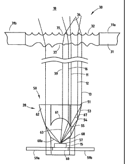
characteristic is to
allow substantial and preferably variable distance to separate the aperture
from the electronic
sensing device. A fifth characteristic is to utilize separate components to
sense the light and
to characterize the angular response characteristic so that the sensor may be
used in a broad
range of applications leading to increased standardization of the light
sensing coinponent.
[0003] Sensor devices of the type used to detect light are constructed in a
variety of packages.
For example, photoresistive sensors are often mounted on a circuit board with
or without a
separate lens positioned in front of the sensor. Some photodiodes have been
constructed in
which the sensor die is mounted to a lead frame and is encapsulated by a clear
epoxy. A
portion of the epoxy encapsulant is molded into a lens so as to focus incident
light onto the
sensor die. Such lenses have been either spherical or other surfaces of
revolution that are
symmetric about an axis which is generally perpendicular to the surface of the
active sensing
element. Unlike a sensor construction in which a separate lens is spaced from
the sensor, the
lens in these types of sensor devices is an integral part of the sensor and
the space separating
the sensor and the lens has been eliminated. The main design difference which
results from
1
CA 02472117 2004-06-25
WO 03/078941 PCT/US03/02193
filling the space between the lens and the sensor with plastic is that the
speed of propagation
of the light rays is reduced being inversely proportional to the index of
refraction of the lens
material. This effectively increases the focal length of the lens in
proportion to the index of
refraction of the material.
[0004] Figs. 4a and 4b illustrate two general sensing configurations, each
with similar
angular response characteristics but with widely differing optical gains. In
the first sensor
configuration in Fig. 4a, the sensor is close to the aperture and has
desirably high optical gain.
Placement of the sensor close to the aperture often leads to the added cost of
additional parts
and assembly processes, and longer electrical connecting patlls to the sensor
often
compromises the electrical design. In the second sensor configuration in Fig.
4b, the sensor is
placed at an appreciable distance from the aperture and has undesirably low
optical gain. The
placement of the sensor may be convenient and less costly but for the overall
design the
reduction in optical gain, wllich may be severe, may compromise or even
prevent satisfactory
performance.
[0005] The angle between lines 41a and 42a and between lines 41b and 42b are
the saine in
each of the illustrative examples and denote the nominal angle between the 50
percent
response points in the optical angular response profile for each of the
sensors. Light blocking
portions of the housing 44a and 45a are depicted in Fig. 4a in fragmentary
view on opposing
sides of the aperture which contains a lens 43a. With the sensing element 48a
placed closer
to the case than the point 49a of intersection of the lines 41 a and 42a which
depict the optical
aperture, the lens, possibly combined with diffusion and/or de-focusing, may
serve to
decrease the viewing aperture from the angle between lines 46a and 47a to that
between lines
41a and 42a as targeted by the design. The lens 43a serves to concentrate
light impinging on
the sensor thereby increasing its optical gain. Thus, the desired reduction in
the overall field
of view is accomplished while increasing the optical gain of the system. The
general
requirement for this to work with a single, thin lens in a non-light piped
mode is for the
sensor 48a to be located closer to the aperture than the apex 49a of the conic
surface depicted
by lines 46a and 47a in Fig. 4a. The conic surface may be non-circular and is
used only as a
temporary gage for illustrative or design purposes. With the lens and/or
filter removed, the
conic surface is aligned in the required viewing direction and inserted as far
as possible into
the aperture opening which is provided. (The regions which are generally
closer to the
2
CA 02472117 2004-06-25
WO 03/078941 PCT/US03/02193
apertures than the points 49a or 49b may be referred to as the near field
regions of the
respective aperture.)
[0006] Light blocking portions of the housing 44b and 45b are depicted in Fig.
4b in
fragmentary view on opposing sides of the aperture which contains a diffusing
lens and/or
surface 43b. In this case, sensor 48b is farther from the aperture than the
apex 49b. The
property of point 49b is similar to that of 49a. Aii alternative way to
describe it is as the point
on the sensor side of the aperture which is the most distant point from the
aperture from
which the full field for which the sensor should respond to incident light or
a substantial
portion thereof may be seen prior to placing an optical element in the
aperture. In this case,
the sensor 48b is more distant from the aperture than the point 49b so that
the angle between
lines 46b and 47b is less than the angle between lines 41b and 42b. In three-
dimensional
terms, the solid angle subtended by the aperture at point 48b where the sensor
is located is
smaller than the solid angle subtended by the aperture at point 49b where the
desired field for
response to incident light may be seen through the aperture with the lens
and/or filter
removed. In this case, an optical element 43b, which has a diffusing effect,
may be
incorporated in the aperture and if the diffusing effect is pronounced enough
to bend enough
rays coming from representative directions 41b and 42b to the extent that they
may strike the
sensor 48b, a balance may be found for wllich the diffusing effect expands the
effective
viewing field from that indicated by the angle between 46b and 47b to that
between 41b and
42b, as required to meet the design objective. The disadvantage is that
instead of
concentrating the light and adding optical gain as was accoinplished in the
first example, the
light level is effectively attenuated because rays that would have come
unobstructed through
the aperture and struck the sensor before placing the diffuser in it are now
spread out by the
disbursing effect of the diffuser so that the proportion of the rays which
reach the sensor is
diminished. Accordingly, there exists the need for a sensor device
construction that may be
placed within a housing a distance from an aperture tllrough the housing
without sacrificing
optical gain.
SUMMARY OF THE INVENTION
[0007] Accordingly, it is an aspect of the present invention to provide a
sensor device that
comprises: a support structure; a sensing element mounted on the support
substrate for
sensing optical radiation and generating an electrical output signal in
response thereto; and
3
CA 02472117 2004-06-25
WO 03/078941 PCT/US03/02193
an encapsulant encapsulating the sensing element on the support structure. The
encapsulant
is configured to define a lens portion for focusing incident optical radiation
onto an active
surface of the sensing element, and an optical radiation collector portion
surrounding the lens
portion for collecting and redirecting optical radiation that is not incident
on the lens portion
onto the active surface of the sensing element.
[0008] According to another embodiment, a sensor assembly comprises: a housing
having an
aperture; a diffusing element positioned across the aperture; and a sensor
device comprising:
a support structure; a sensing element mounted on the support structure for
sensing optical
radiation and generating an electrical signal in response thereto; and an
encapsulant
encapsulating the sensing element on the support structure, the encapsulant
being configured
to define an optical radiation collector portion having a parabolic reflecting
surface for
collecting and redirecting incident optical radiation towards the sensing
element by total
internal reflection.
[0009] According to another embodiment, a vehicle accessory for mounting in a
vehicle is
provided that comprises: a sensor device comprising: a support structure; a
sensing element
mounted on the support structure for sensing optical radiation and generating
an electrical
output in response thereto; and an encapsulant encapsulating the sensing
element on tlle
support structure. The encapsulant is configured to define a lens portion for
focusing incident
optical radiation onto an active surface of the sensing element, and an
optical radiation
collector portion surrounding the lens portion for collecting and redirecting
optical radiation
that is not incident the lens portion onto the active surface of the sensing
element.
[0010] According to another embodiment, a veliicle accessory for mounting in a
vellicle is
provided that comprises: a housing having an aperture; a diffusing element
positioned across
the aperture; and a sensor device comprising: a support structure; a sensing
element mounted
on the support structure for sensing optical radiation and generating an
electrical signal in
response thereto; a.nd an encapsulant encapsulating the sensing element on the
support
structure, the encapsulant being configured to define an optical radiation
collector portion
having a parabolic reflecting surface for collecting and redirecting incident
optical radiation
towards the sensing element by total internal reflection.
[0011] According to another embodiment, a sensor device comprises: a support
structure; a
sensing element mounted on the support stnicture for sensing optical radiation
and generating
4
CA 02472117 2004-06-25
WO 03/078941 PCT/US03/02193
an electrical output in response thereto; and an encapsulant encapsulating the
sensing element
on the support structure, the encapsulant including an integral lens for
directing incident
optical radiation toward the sensing element; and a light collector
surrounding the integral
lens for collecting and redirecting optical radiation that is not incident the
lens onto the active
surface of the sensing element.
[0012] These and other features, advantages, and objects of the present
invention will be
fiuther understood and appreciated by those skilled in the art by reference to
the following
specification, claims, and appended drawings.
BRIEF DESCRIPTION OF THE DRAWINGS
[0013] In the drawings:
[0014]' Fig. 1 is a perspective view of a sensor device constructed in
accordance with the
present invention;
[0015] Fig. 2 is a side cross-sectional view of the sensor device sllown in
Fig. 1 illustrating
various light ray tracings that first pass through a diffuser;
[0016] Fig. 3 is a top plan view of a lead frame component used to construct
several sensor
devices in accordance with the present invention;
[0017] Fig. 4a is a side view of a sensor device disposed close to an aperture
in which a lens
is disposed;
[0018] Fig. 4b is a side view of a sensor device disposed farther from an
aperture in which a
diffuser is disposed;
[0019] Fig. 4c is a side view of a sensor device according to the present
invention, which is
spaced a substantial distance from an aperture in which a diffuser is
disposed;
[0020] Fig. 5 is an electrical circuit diagram in block and schematic form
showing circuitry
permitting a processing circuit and a sensing element, which may be used in
the inventive
sensor device structure to be interconnected by a single line carrying both
sensitivity control
and sensor output;
[0021] Fig. 6 is a schematic diagrain of a light-to-pulse circuit for use in
the sensing element
CA 02472117 2004-06-25
WO 03/078941 PCT/US03/02193
shown in Fig. 5;
[0022] Fig. 7 is a timing diagram illustrating operation of the light-to-pulse
circuit of Fig. 6;
[0023] Fig. 8 is a schematic diagram of an optional light-to-pulse circuit
with noise
compensation for use in the sensing element shown in Fig. 5;
[0024] Fig. 9 is a tiining diagram illustrating operation of the light-to-
pulse circuit of Fig. 8;
[0025] Fig. 10A is an elevational view of the front of a rearview mirror
assembly
incorporating the sensor device of the present invention;
[0026] Fig. l OB is an elevational view of the rear of a rearview mirror
assembly
incorporating the sensor device of the present invention;
[0027] Fig. l OC is a top plan view of the rear of a rearview mirror assembly
incorporating the
sensor device of the present invention;
[0028] Fig. 10D is an elevational view of the side of a rearview mirror
assembly
incorporating the sensor device of the present invention;
[0029] Fig. 11 is an electrical circuit diagram in block fomi illustrating a
vehicle equipment
control system employing the sensor device of the present invention; and
[0030] Fig. 12 is a side elevational view of a moisture detecting system
employing the sensor
device of the present invention.
DETAILED DESCRIPTION OF THE PREFERRED EMBODIMENT
[0031] Reference will now be made in detail to the present preferred
embodiment of the
invention, an example of which is illustrated in the accompanying drawings.
Wherever
possible, the saine reference numerals will be used throughout the drawings to
refer to the
same or like parts.
[0032] A sensor device 50 constructed in accordance with the present invention
is shown in
Fig. 1 and a sensor assembly 10 incorporating sensor device 50 is shown in
Fig. 2. The
sensor device 50 includes a support structure, such as a printed circuit board
or a lead frame
60, an integrated circuit including a sensing element 15 having an active
sensing area 57
6
CA 02472117 2004-06-25
WO 03/078941 PCT/US03/02193
mounted on the support substrate for sensing optical radiation, preferably
visible light, and an
encapsulant 62 encapsulating the sensing element on the support structure. In
general, the
encapsulant 62 defines a lens structure 20 including an integral refracting
lens portion 61
preferably having an elliptical refracting surface for focusing incident
optical radiation onto
active surface 57 of sensing element 15. Lens structure 20 further includes an
optical
radiation collector portion 53 surrounding the lens portion 61 for collecting
and redirecting
optical radiation that is not incident on lens portion 61 onto the active
surface 57 of sensing
element 15. The optical radiation collecting portion 53 includes a parabolic
reflecting surface
54 that redirects incident optical radiation towards sensing element 15 by
total internal
reflection. Optical radiation collecting portion also includes an annular
optical radiation
receiving surface 51 that lies in a plane perpendicular to the major axis of
elliptical lens
portion 61 and is disposed around elliptical lens portion 61.
[0033] Sensor assembly 10 further includes a diffuser and aperture subassembly
30 that
includes an aperture formed in a housing enclosure 31 and a diffuser 32
disposed in the
aperture formed in enclosure 31. Having generally described the structure of
the sensor
assembly of the present invention, a description of the optical properties,
functions, and
advantages of such structure is provided below.
[0034] In the sensor configuration shown in Fig. 4c, a sensor constructed as
described above
is placed at an appreciable distance from the aperture and has desirably high
optical gain.
Features which lead to this desirable combination are portions of the
invention described
herein.
[0035] In the illustration in Fig. 4c, the positioning and definition of 49c
is similar to that for
49a and 49b (Figs. 4a and 4b), and the positioning of the small area sensing
element 15 is
similar to that of 48b. Other corresponding features are also conlparable
except that a lens
structure which preferably encapsulates and preferably surrounds sensor 15 is
added and lens
and/or diffusing eleinent 32 is designed to generally obtain the desired
profile of sensitivity
versus angle for the total systein. The resulting system gives substantially
enhanced optical
gain over that in Fig. 4b.
[0036] The lens structure 20 fiinctions to project light rays entering through
the aperture onto
the active area 57 of sensor 15 filling a substantial portion of a relatively
large cone angle, the
extremes of which are depicted by lines 46c and 47c in the illustrative
example. The lens
7
CA 02472117 2004-06-25
WO 03/078941 PCT/US03/02193
does not need to preserve imaging integrity but in some other respects
parallels low F number
photographic lens. It is also preferable to have an even lower F number than
is normally
practical with imaging optics. In the preferred structure, a majority of the
rays of which 45c
are representative which are focused by the lens structure 20 onto the sensor,
originate from
the desired field of view and enter the systein tlirougli the aperture.
Preferably rays, such as
44c, which do not enter through the aperture, make up a small to negligible
portion of the
light which the lens directs to the active area of the sensor 15. In the
foregoing, particularly
when the angle between 41c and 42c is large, only a sampling of these rays
will typically be
directed to the active sensing area, but it is preferable that the majority of
the rays which are
directed to the active sensing area come from the directions for which the
light level is to be
measured. The lens and/or diffusing unit 32 is designed to have a dispersing
effect so that a
representative proportion of rays emanating from within the field delimited by
the direction
of 41 c and 42c in the illustrative example are brought to an alignment
whereby they are
focused by the lens structure 20 onto the active area of sensor 15. It is
preferable that both
the distribution and the extent of the scattering profile of the diffuser be
such that the angle
dependent magnitude and the general extremes of the response profile for the
optical system
meet design objectives. Since increased scattering reduces the overall optical
gain, it is also
preferable that the degree of scattering be reasonably close to the minimum
aniount needed to
meet the response profile objectives.
[0037] In some embodiments of the invention, optical subassembly 30 may
include a single
negative or even a positive lens element. It is, however, preferable to have
finer patterns.
The pattern may be, for example, repetitious or random in the diffusing effect
and produced
by a fine array of small lens elements by a diffusant which is disbursed in
the material which
covers the aperture by a randomly or irregularly grained surface or even by an
ultra fine
structure which may be generated by replicating a micro pattern. A micro
pattern may be
generated by laser interference patterns and such diffusers may in turn employ
interference
patterns generated by the fine features of the optical surface in addition to
or in place of
reflective or refractive effects to achieve the desired light disbursing
effect.
[0038] As shown in Fig. 2, light enters through aperture and diffuser
subassembly 30 and
after traveling some distance, a portion of the entering rays strike the lens
structure 20 of
sensor device 50 where a portion of the rays which strike the sensor are
directed to the light
8
CA 02472117 2004-06-25
WO 03/078941 PCT/US03/02193
sensing area 57 on sensing element 15. Leads 59a-59d are electrically attached
to the sensing
element 15 and to an associated electrical circuit 66 (Fig. 5), which
functions to read or
otherwise respond to the level of the light which strikes the sensor. The
diffuser and aperture
subassembly 30 functions to shape the directional or spatial response profile
of the sensor so
that the profile of sensitivity versus direction is satisfactory for the
application. For some
embodiments of this invention, the lens structure 20 in sensor device 50 is
designed so that it
serves to direct a large enough proportion of the rays which emanate from the
diffusing
element and strike the sensor on the light sensing area of the chip to make
the overall optical
gain of the system comparable to or in some instances greater than that which
is normally
attained when the sensor is positioned close to the sensing aperture, i.e. in
the near field
region. With the sensor positioned in the near field area, it is often readily
possible to direct
light from the field of view so that it fills a relatively large solid angle
as it impinges on the
active area of the sensor and thereby contributes to the overall optical gain.
In the design of
Fig. 2, it is desirable to provide a design which maintains reasonable,
perhaps comparable or
better optical efficiency throughout a range of positioning options for the
sensing eleinent
which may in some instances include the near field but which may in others
extend to a much
greater distance from the aperture than the farthest extent of the near field.
One way to
practice the invention is to provide a lens system which directs rays which
emanate from the
diffusing element to the light sensitive element 15 and to generally fill an
effective solid
angle which is comparable in size to that of the comparable system in the near
field with
these rays. In the discussion, the active region 57 of the sensor is more
sensitive to rays
which enter from some directions or positions on the active surface than from
others, and the
net effect on the output of a ray which strikes the active area of the sensor
is equal to the
product of the intensity of the ray with the efficiency with which a ray
entering at the
particular angle and at the particular position on the sensor surface is
received by the sensor.
This may be referred to as the response efficiency for responding to liglit to
the particular
point on the sensor and coming from a particular angle relative to the sensor.
The lenses or
combination of lenses and diffusing elements may also vary in the efficiency
with which they
direct rays to particular entrance angles and positions and this may be
referred to as the
collection efficiency for directing light to the particular point on the
sensor and coming from
a particular angle relative to the sensor. Thus, for a particular angle and
point of entry, a
9
CA 02472117 2004-06-25
WO 03/078941 PCT/US03/02193
reception efficiency may be defined as the product of the response efficiency
and the
collection efficiency. It would be most accurate to integrate the reception
efficiency over the
solid angle through which light enters the active sensing area and to use this
integrated
reception angle perhaps instead of the solid angle as a basis for comparison
of the optical
systems. The general point is that it is a desirable feature of the invention
to generally fill a
large solid angle relative to the sensing element 15 with light and for this
solid angle to
generally include the regions of high sensitivity of the sensor to incoining
light. Since the
sensor may have an approximate cosine response characteristic for which the
response
efficiency is highest for nonnal rays and for which the response approaches
zero for rays
which are nearly parallel or tangent to the sensing surface, it is generally
preferable to favor
directions normal to the sensing surface for the portions of the total solid
angle over which
incident rays are directed to the sensor. The angle between lines 68 and 68a
generally
denotes the outer extent of the cone angle over which rays are collected in
the illustrative
embodiment. As will be discussed later, a rib to encapsulate the lead franle
connections
prevents filling of some portions of the cone delimited by lines 68 and 68a.
[0039] In the illustrative diffuser and aperture assembly 30, fragmentary
portions 31a and
31b of the preferably opaque housing enclosure 31 are shown. Surface 35 of
diffuser 32
contains generally parallel grooves. These grooves serve to increase the
dispersion of light in
a direction generally parallel to the sheet of paper. The lower surface 37 of
diffuser assembly
30 is an irregular surface which serves to diffuse the light approximately
equally in every
direction. Ray 34 is refracted at surfaces 35 and 37, and continues as ray 39
through
refracting lens 61 which focuses it as ray 63 onto the active sensing surface
57. Ray 16 is
likewise refracted by lens 61 and focused onto the active area 57. Ray 16 is
closer than ray
39 to the outer extent 55 of the refracting lens 61. Rays 11, 12, and 13 enter
the upper surface
of lens structure 20 and are reflected by total internal reflection at
reflecting surface 54
strildng the active sensing area 57. The order of the reflected rays is
reversed from the order
of the incoming rays. The lens 61 is set at a depth such that the outer
reflected ray 67 just
misses the edge 55. In the lens structure 20, the refracting portion 61 fills
in the center
portion of the cone of rays which is directed toward active sensing area 57.
The parabolic
reflecting surface 54 fills in the outer proportion of the cone. The combined
reflecting and
refracting lenses coinplement each other to generally fill the area between
lines 68 and 68a.
CA 02472117 2004-06-25
WO 03/078941 PCT/US03/02193
The resulting dispersion is greater in the direction parallel to the paper due
to the combined
and generally additive effects of the unidirectional dispersion of surface 35
and the multi-
directional dispersion of surface 37. The result is a sensor with a
substantially wider field of
view in the direction parallel to the paper than in the direction
perpendicular to the paper.
0040] The integrated sensing element circuit 15, of wliich the active sensing
area 57 is a
part, is attached to lead frame 60. The active sensing area 57 may be small,
for example, 100
microns in diameter. The sensing area is shown as a raised portion in the
illustration only to
make it stand out. In the actual part, it is likely to be flush or even very
slightly recessed.
The attachtnent of sensor circuit 15 to lead frame 60 may be made using
conductive epoxy
completing one of the electrical connections with the other connections
completed by lead
bonds or, alternately, all of the connections may be made with lead bonds.
Leads 59a-59d
extend from the package to make electrical coimection to the printed circuit
board and to
attach the part to the printed circuit board.
[0041] Fig. 1 is an isometric drawing of the sensor device 50. Representative
ray 112 enters
the top surface 51 and is reflected by total internal reflection at surface 54
to the active
sensing area 57 of the sensor element 15. Lilcewise, ray 112a is reflected by
a similar surface
at the back of the device and also strikes the active sensing area. Ray 113
enters through the
recessed refracting lens 61 and is focused to the active sensing area. Rib
portion 104 serves
to house the lead frame and allow clearance for the mold to be retracted from
the part.
Section 106 is one of two sections of the rib which is widened to provide
support for the leads
59a and 59b. Leads 59c and 59d extend from the symmetrically placed enlarged
section
106a. The dashed lines 111 are included for illustrated purposes to delimit
areas 110 and
110a. The areas are above the ribs 104 and 104a which join with the parabolic
reflector 54.
Rays entering this area are not generally directed to the active sensing area.
The part is
preferably made in a two-part mold which has parting lines generally depicted
by
representative lines 107, 107a, and 107b.
j0042] Fig. 3 illustrates a portion of a lead frame subassembly 60 on whicli
integrated sensor
element circuit 15 has been bonded. Only four of the devices have been shown.
The actual
assembly would include the number of devices, perhaps 64, which would fit in
one of the
transfer mold sections. The lead frame assembly includes holes, of wliich 73
is
representative, wliich are used for locating and holding the lead frame during
the asseinbly
11
CA 02472117 2004-06-25
WO 03/078941 PCT/US03/02193
processes. Element 74 of the lead frame subassembly provides two connecting
pins 74a and
74b and a pad 74c on which the silicon sensor element circuit 15 is mounted.
The element 74
also serves as the cross-connecting link to hold the lead frame assembly
together prior to
separation of the parts. The dashed rectangles of which 71 is representative
denote the areas
that are punched out in order to separate the parts after the molding process
is complete.
Lead bond wires 76 and 78 coimect bonding pads on the silicon sensor circuit
15 to
comlecting pins 75 and 79, respectively. Upon separation of the devices, pins
74a and 74b
serve as leads 59c and 59b, respectively, while pins 75 and 79 serve as leads
59d and 59a,
respectively. The circular eleinent 20 depicts the outline feature of the
plastic lens which will
be molded over the part. After the light sensing dies are bonded to the lead
frame and
connections are made, the lead frame is placed in a transfer mold and the
plastic lens
assembly depicted in Fig. 1, 2, and 4c is transfer molded onto the lead frame.
The lens has
the advantage of being in one piece and serving to encapsulate the part. It
may also be
molded with a conventional two-part mold. After the parts are molded, they are
cut apart and
de-flashed to form individual parts as depicted in Fig. 1.
[0043] In the preferred configuration, the lens system is designed to focus
light entering from
a narrow beam angle which is approximately parallel to the axis of the lens
system onto the
active sensing area. For this system, the reflecting portion is a parabola
whose focus is
approximately centered on the light sensitive area of the receiver. The
refracting lens is
preferably elliptical in shape, being designed to focus light rays which are
parallel to the axis
of the system onto the center of the light sensitive area. An elliptical
shaped lens having its
major axis coincident witlz the axis of the lens system, having the foci which
is most distant
from the tip of the lens coincident with the center of the ligllt sensing
area, and having a ratio
of major diameter to minor diameter chosen to give the best focus for light of
a color for
which the system is optimized is a design choice which will serve this purpose
well. The
focal length of the parabola is chosen so that rays parallel to the axis of
the lens which strike
the active portion of the parabola at points wliich are closest to the center
axis of the lens are
reflected at an angle which fills in the outer extent of the cone of light
which the optical
system is designed to focus onto the sensor. When the location of the focus of
the ellipse and
the alignment of the major axis and the ratio of the major diameter to the
minor diameter are
chosen as outlined above, one is still free to scale the overall size of the
ellipse. It is
12
CA 02472117 2004-06-25
WO 03/078941 PCT/US03/02193
preferable to scale the size of the ellipse so that the outer edge of the
elliptical lens is just high
enough in the lens structure to clear rays which are reflected to the sensing
surface from the
outermost extent of the parabolic surface. As the diameter of the refracting
lens is increased,
the slope at its, outer extent becomes too high. Stated another way, there is
a maxiinum
practical cone angle which can be filled by a single surface lens made of a
material of a given
refractive index. This is the major factor which influences the choice of the
balance between
the diameter of the refracting lens and the diameter of the parabolic
reflector. The overall
size of the lens assembly may be scaled. It should not be so small that
tolerances are
unnecessarily tight and also needs to be large enough that the encapsulated
sensor assembly
will fit under the refracting lens. Also, the parabolic reflector needs to be
large enough that
the area taken from the reflector by the rib which encapsulates the connecting
leads is not an
undesirably large proportion of the total reflector area. Example dimensions
are as follows:
the semi-major dianieter of elliptical lens 61 is 1.529 intn and the semi-
minor diameter of
elliptical lens 61 is 1.163 inm; the focal length of parabolic reflector 54 is
0.2887 mm; the
radius of refracting lens 61 is 1.0 mm; the radius of parabolic reflector 54
at top is 2.2 nnn;
and the index of refraction of the plastic encapsulant 62 is 1.54.
[0044] The encapsulant 62 may be made of single material or may be made of
more than one
material as disclosed in commonly assigned U.S. Patent Publication No. US 2002-
0056806,
published on May 16, 2002, entitled "SENSOR DEVICE HAVING AN ANAMORPHIC
LENS."
[0045] The sensing element 15 may be any form of photosensor device such as a
photodiode, cadmium sulfide CdS cell, etc. A preferred sensing element is the
photodiode disclosed in commonly assigned U.S. Patent No. 6,379,013 entitled
"VEHICLE EQUIPMENT CONTROL WITH SEMICONDUCTOR LIGHT
SENSOR," and U.S. Patent No. 6,359,274 entitled "PHOTODIODE LIGHT
SENSOR." A brief'disclosure of the structural components of the sensing
element
circuitry and of a processing circuit 66 that interfaces with sensing element
15 is
discussed below with reference to Figs. 5-9.
[0046] Referring now to Fig. 5, the processing circuit 66 and sensing element
15 will be
described in greater detail. The processing circuit 66 and sensor element 15
are
interconnected by a single line 164 that carries interconnect signals 186,
which can
13
CA 02472117 2004-06-25
WO 03/078941 PCT/US03/02193
advantageously include both light sensor sensitivity control signals and
resultant light sensor
output signals. A microcontroller may be used to implement processing circuit
66 and would
include a transistor element Q1 and a buffer 192 connected to an output pin
188, or other
input/output (I/O) pin structure, which is connected to signal line 164. The
transistor element
Q1 may be implemented using a suitable transistor such as a field effect
transistor (FET)
connected between signal pin 188 and ground. Transistor Ql is controlled by
control line
190, which is connected to the base of transistor Q1. Buffer 192 is also
connected to signal
pin 188 to isolate the signal line 164 from signal levels present in the
microcontroller.
[0047] As described above, the sensor device includes an encapsulant 62
including a lens 61
for admitting light 176 incident on an exposed ligllt transducer 178.
Encapsulant 62 also
admits and retains power pin 180, ground pin 182, and signal pin 184, which
are preferably
part of lead frame 12. The use of only three pins 180, 182, and 184 greatly
reduces the cost
of sensing element 15 and associated processing circuit 66.
[0048] Sensing element 15 is connected to processing circuit 66 through bus
164, which carries
intercomlection signal 186 between signal pin 184 in sensing element 15 and
signal pin 188 in
processing circuit 66. As will be described below, signal pins 184, 188 are
tri-state ports permitting
interconnect signal 186 to provide both an input to sensing element 15 and an
output from sensing
element 15.
[0049] Within sensing element 15, transistor Q2, which can be impleinented
using a suitable
transistor such as an FET element, is connected between signal pin 184 and
ground.
Transistor Q2 is controlled by output pulse 194 connected to the gate of Q2.
Constant current
source 196 is connected to signal pin 184 so that if neither transistor Q1 nor
transistor Q2 are
ON (high logic level), intercoimect signal 186 is pulled to a high logic
level. Constant
current source 196 nominally sources about 0.5 mA to pull up interconnect
signal 186. The
input of Schmidt trigger inverter 198 is connected to signal pin 184.
Inverters 200 and 202,
which are comiected in series, follow Schmidt trigger inverter 198. The output
of inverter
202 clocks D flip-flop 204. The output of inultiplexer 206 is connected to the
D input of flip-
flop 204. The select input of multiplexer 206 is driven by output pulse 194
such that when
output pulse 194 is asserted, the D input of flip-flop 204 is unasserted, and
when output pulse
194 is not asserted, the D input of flip-flop 204 is asserted. The output of
NAND gate 208 is
com7ected to low asserting reset 210 of flip-flop 204. The output of flip-flop
204 is
14
CA 02472117 2004-06-25
WO 03/078941 PCT/US03/02193
integration pulse 212. Integration pulse 212 and the output of inverter 200
are inputs to
NAND gate 208. Light-to-pulse circuit 214 accepts integration pulse 212 asld
the output of
exposed light transducer 178 and produces output pulse 194.
[0050] Sensing element 15 may advantageously include a shielded light
transducer 216,
which does not receive light 176. Shielded light transducer 216 has
substantially the same
construction as exposed light transducer 178, being of the same size and
material as
transducer 178. Light-to-pulse circuit 214 uses the output of shielded light
transducer 216 to
reduce the affects of noise in exposed light transducer 178.
[0051] Fig. 6 is a schematic diagram illustrating the light-to-pulse circuit
214, which includes
exposed light transducer 178 for converting light 176 incident on exposed
light transducer
178 into charge accumulated in light storage capacitor 304, indicated by CSL.
Exposed light
transducer 178 may be any device capable of converting light 176 into charge,
such as the
photogate sensor described in U.S. Patent No. 5,471,515 entitled "ACTIVE PIXEL
SENSOR
WITH INTRA-PIXEL CHARGE TRANSFER" to E. Fossum et al. Preferably, light
transducer 178 is a photodiode such as is described below. Except as noted,
the following
discussion does not depend on a particular type or construction for exposed
light transducer
178.
[0052] Light-to-pulse circuit 214, wliich is connected to transducer 178,
receives an integration
pulse 212, and outputs a light comparator signal which is proportional to the
amount of light
176 impacting transducer 178 during integration period pulse 212. Light-to-
pulse circuit 214
operates under the control of sensor logic 306. Sensor logic 306 generates
reset signa1308
controlling switch 310 connected between exposed light transducer output 312
and VDD.
Sensor logic 306 also produces sample signa1314 controlling switch 316 between
exposed light
transducer output 312 and light storage capacitor 304. The v,oltage across
light storage
capacitor 304, light storage capacitor voltage 318, is fed into one input of
comparator 320. The
other input of comparator 320 is ramp voltage 322 across ramp capacitor 324.
Ramp capacitor
324 is in parallel with current source 326 generating current IR. Sensor logic
306 further
produces ramp control signal 328 controlling switch 330 connected between ramp
voltage 322
and VDD. Comparator 320 produces comparator output 194 based on the relative
levels of light
storage capacitor voltage 318 and ramp voltage 322. Sensor logic 306 may
generate reset
signal 308, sample signa1314, and ramp control signa1330 based on internally
generated
CA 02472117 2004-06-25
WO 03/078941 PCT/US03/02193
timing or on externally generated integration pulse 212.
[0053] Referring now to Fig. 7, a timing diagram illustrating operation of the
light-to-pulse
circuit 214 of Fig. 6 is shown. A measurement cycle is started at time 340
when sample
signa1314 is asserted while reset signa1308 is asserted. This closes switch
316 to charge
light storage capacitor 304 to VDD as indicated by voltage leve1342 in light
storage capacitor
voltage 318. Reset signa1308 is then deasserted at time 344, opening switch
310 and
beginning integration period 346. During integration period 346, light 176
incident on
exposed light transducer 178 generates negative charge causing declining
voltage 348 in light
storage capacitor voltage 318. At time 350, ramp control signa1328 is asserted
closing
switch 330 and charging ramp capacitor 324 so that ramp voltage 322 is VDD as
indicated by
voltage leve1352.
[0054] Sample signal 314 is deasserted at time 354, causing switch 316 to
open, thereby
ending integration period 346. At some time 356 following time 354 and prior
to the next
measurement cycle, reset signal 308 inust be asserted closing switch 310. At
time 358, ramp
control signal 328 is deasserted opening switch 330. This causes ramp
capacitor 324 to
discharge at a constant rate through current source 326 as indicated by
declining voltage 360
in ramp voltage 322. Initially, as indicated by voltage leve1362, comparator
output 332 is
unasserted because ramp voltage 194 is greater than light storage capacitor
voltage 318. At
time 364, declining voltage 360 in ramp voltage 322 drops below light storage
capacitor
voltage 318 causing comparator output 194 to become asserted. Comparator
output 194
remains asserted until time 366 when rainp control signa1328 is asserted
closing switch 330
and pulling ramp voltage 322 to VDD. The difference between time 366 and time
364,
indicated by pulse duration 368, is inversely related to the amount of light
176 received by
exposed light transducer 178 during integration period 346. The integration
period 346 can
be set directly by the integration pulse 212 or a signal derived from
integration pulse 212. It
is envisioned that the integration period 346 will be proportional to the
width of the
integration pulse 212, which is proportional to the pulse width of the control
line signal 190
in the circuit of Fig. 5.
[0055] Fig. 8 is a schematic diagram of a modified liglit-to-pulse circuit
214a with noise
compensation. Modified light-to-pulse circuit 214a improves upon light-to-
pulse circuit 214
by incorporating shielded light transducer 216 and associated electronics.
Shielded light
16
CA 02472117 2004-06-25
WO 03/078941 PCT/US03/02193
transducer 216 preferably has the same construction as exposed light
transducer 178.
However, shielded light transducer 216 does not receive light 176. Charge
generated by
shielded light transducer 216, therefore, is only a function of noise. This
noise is
predominately thermal in nature. By providing shielded light transducer 216
having the same
construction as exposed light transducer 178, such that the exposed and
shielded transducers
have the same surface area and material coinposition and may be deposited on
the same die,
the noise signal produced by shielded light transducer 216 will closely
approximate the noise
within the signal produced by exposed light transducer 178. By subtracting the
signal
produced by shielded light transducer 216 from the signal produced by exposed
light
transducer 178, the effect of noise in light transducer 178 can be greatly
reduced.
[0056] Reset signa1308 controls switch 382 connected between shielded
transducer
output 384 and VDD. Sample signal 314 controls switch 386 connected between
shielded
transducer output 384 and noise storage capacitor 388 indicated by CSN. The
noise
storage capacitor voltage 390, which is the voltage across noise storage
capacitor 388, is
one input to comparator 392. The second input to comparator 392 is ramp
voltage 322.
The outputs of coinparator 392, noise comparator output 394, and comparator
output 194
serve as inputs to exclusive-OR gate 396. Exclusive-OR gate 396 generates
exclusive-
OR output 194 indicating the intensity of light 176.
[0057] Fig. 9 shows a timing diagram illustrating operation of the light-to-
pulse circuit 214a
of Fig. 8. Light-to-pulse circuit 214a functions in the same manner as light-
to-pulse circuit
214 with regard to reset signal 308, sample signa1314, light storage capacitor
voltage 318,
ramp voltage 322, ramp control signal 328, and comparator output 194. At time
340, sample
signa1314 is asserted while reset signal 308 is asserted. Switches 382 and 386
are both
closed charging noise storage capacitor 388 to VDD as indicated by voltage
level 410 in noise
storage capacitor voltage 390. At time 344, reset signa1308 is deasserted
opening switch 382
and causing declining voltage 412 in noise storage capacitor voltage 390 from
charge
produced by shielded light transducer 216 due to noise. At time 354, sa.inple
signal 314 is
deasserted ending integration period 346 for noise collection. At time 358,
ramp control
signal 328 is deasserted causing declining voltage 360 in ramp voltage 322.
Initially, as
indicated by voltage level 414, noise comparator output 394 is unasserted
because ramp
voltage 322 is greater than noise storage capacitor voltage 390. Since
comparator output 332
17
CA 02472117 2004-06-25
WO 03/078941 PCT/US03/02193
is also unasserted, output 194 from comparator 396 is unasserted as indicated
by voltage level
416. At time 418, ramp voltage 322 drops below the level of noise storage
capacitor voltage
390, causing noise comparator output 394 to become asserted. Since noise
comparator output
394 and comparator output 332 are different, output 194 from comparator 396 is
asserted. At
time 364, ramp voltage 322 drops beneath the level of light storage capacitor
voltage 318,
causing comparator output 194 to become asserted. Since both noise comparator
output 394
and comparator output 194 are now asserted, output 194 from exclusive-OR gate
396 now
becomes unasserted. The difference between time 364 and time 418, output pulse
duration
420, has a time period proportional to the intensity of light 176 incident on
exposed ligllt
transducer 1781ess noise produced by shielded light transducer 216 over
integration period
346. The duration between time 418 and time 358, noise duration 422, is
directly
proportional to the amount of noise developed by shielded light transducer 216
over
integration period 346. Since the majority of this noise is thennal noise,
noise duration 422 is
indicative of the temperature of shielded light transducer 216. At time 366,
ramp control
signa1328 is asserted, deasserting both noise comparator output 394 and
comparator output
194.
[0058] In circuits where very high light levels may impinge on the sensor, it
is preferable to
include a comparator (not shown) to end the output pulse when the voltage 318
falls below a
predetermined tllreshold. This has the effect of limiting the maximum duration
420 of the
output pulse at signal 194.
[0059] Additional details of the operation of processing circuit 66, sensing
element 15, and
light-to-pulse circuits 214 and 214a are disclosed in the above referenced
U.S. Patent
Nos. 6,379,013 and 6,359,274.
[0060] Although a specific and preferred example of a sensing element is
disclosed above,
the term "sensing element" as used herein is not limited to any such
structure, but rather may
include a form of photosensor. Similarly, although the "support structure" is
described above
as being a lead frame or portion thereof, the support structure may be any
structure on wliich
a sensing element may be supported and encapsulated.
[0061] The sensor device of the present invention may be used in many of the
applications in
18
CA 02472117 2008-01-28
which conventional sensor devices are employed. Commonly assigned U.S. Patent
No.
6,379,013 discloses various automotive applications of such sensors.
[0062] Figs. l0A-lOD, 11, and 12 show several such automotive applications.
Specifically, a
rearview mirror assembly 500 is shown in Figs. 10A-10D, which incorporates an
electrochromic realview mirror 502 that has a reflectivity that is controlled
by a processing
circuit 66 (Figs. 5 and 11) as a function of an ambient light level sensed by
a forward facing
ambient sensor l0a (Fig. lOB) and a reaiward facing glare sensor l Ob (Fig.
10A). Either one
or both of sensors I Oa and I Ob may have any of the constructions shown in
Figs. 1-4. By
utilizing a sensor having the construction shown in either of Figs. 1-4, the
liorizontal field of
view may be widened or narrowed relative to the vertical field of view as may
be desirable
for the particular sensor.
[00631 As shown in Figs. 10B-IOD, the rearview mirror may further include a
sky sensor
lOc that is aimed upward at the sky. Such a sky sensor is useful in a headlamp
control
system for detecting tunnels and thereby ensures that headlamps are
appropriately turned on
when the vehicle is in a tunnel and turned off upon exiting the tunnel. Sky
sensor 10c may
also advantageously employ the construction shown in Fig. 1 and described
above. Sky
sensor lOc is coupled to a processing circuit 66 (Figs. 5 and 11) which, in
turn, may be
coupled to a headlamp control unit 512 to thereby turn the vehicle headlamps
on and off in
response to the ambient light level and sky light level sensed by sensors l0a
and lOc. The
headlamp control system may further include an image sensor 515 for sensing
images
forward of the vehicle for purposes of controlling the brightness of the high
beam headlamps
and/or activating or aiming the headlamps or other exterior lights 516 to
change the beam
pattern produced by the exterior lights based upon light sources detected by
the image sensor
515. An example of such a headlamp control system is disclosed in commonly
assigned U.S.
Patent No. 6,587,573 filed on March 5, 2001, entitled "SYSTEM FOR CONTROLLING
EXTERIOR VEHICLE LIGHTS" filed by Joseph S. Stam et al. The output of the
sensors
10a, lOb, and/or lOc may also be used to control other vehicle lights such as
the interior
lights 518 of the vehicle and more particularly to control the brightness of
the display lights
of the various displays in the instrument panel and other vehicle accessories.
[0064] As also shown in Figs. 10B- l OD, two or more additional sensors 10d
and l0e may be
19
CA 02472117 2004-06-25
WO 03/078941 PCT/US03/02193
employed to sense sun loading. Sun loading sensors l Od and 10e are aimed
upward toward
the slcy above the vehicle and are aimed slightly to different sides of the
vehicle to sense
whether the sun load on one side of the vehicle is greater than on the other
side of the vehicle.
A processing circuit 66 (Figs. 5 and 11) is coupled to sun load sensors lOd
and l0e and is
coupled to a climate control system 530 of the vehicle for adjusting the fan
speeds and/or
temperature settings for respective sides of the vehicle based upon the light
levels sensed by
the sun load sensors lOd and 10e. Sun load sensors lOd and l0e may also be
configured as
described above and shown in Figs. 1-4. The light levels sensed by any one of
the above
sensors may be used to control some aspect of the operation of climate control
system 530.
For example, sky sensor 10c and ambient sensor 10a may be used to detect an
approaching
tunnel to thereby cause the headlamps to turn on and the climate control to
enter a
recirculation mode.
[0065] Fig. 12 shows yet another automotive application for utilizing the
inventive sensor
construction. Specifically, Fig. 12 shows a moisture sensing system for
detecting moisture
(i.e., rain, mist, fog, frost, and snow) on the vehicle windshield. The system
includes a light
source such as an LED 540 and a sensor 10f. Optical radiation (i.e., visible
light, or infrared
or ultraviolet radiation) emitted from LED 540 enters the windshield 550 and
is internally
reflected therein and exits to impinge upon sensor 10f. If moisture is present
on the
windshield, the light from LED 540 does not reach sensor 10f and a processing
circuit 66
(Figs. 5 and 11) actuates the vehicle windshield wipers 545 via wiper
contro1546 and/or the
windshield defogger of the vehicle climate control system 530.
[0066] While the above exainples of automotive applications are described as
being disposed
in a rearview mirror assembly, it will be appreciated that some of the above
applications may
be implemented, in wliole or in part, in other locations or vehicle
accessories in the vehicle,
such as the vehicle instrument panel, an A-pillar, a sun visor, or in a.n
overhead console
located on the headliner or on or near the windshield. Additionally, the
sensor of the present
invention may be employed in any other non-automotive application and the
invention as
broadly defined is not limited to any such application.
[0067] The above description is considered that of the preferred embodiment
only.
Modifications of the invention will occur to those skilled in the art and to
those who make or
CA 02472117 2004-06-25
WO 03/078941 PCT/US03/02193
use the invention. Therefore, it is understood that the embodiments shown in
the drawings
and described above are merely for illustrative purposes and not intended to
limit the scope of
the invention, which is defmed by the following claims as interpreted
according to the
principles of patent law, including, the doctrine of equivalents.
21