Note: Descriptions are shown in the official language in which they were submitted.
CA 02472231 2010-04-15
74842-47
INTEGRATED CIRCUIT AND EMBEDDED CIRCUITRY
INITIALIZATION AND PROCESSING
TECHNICAL FIELD OF THE INVENTION
The invention relates generally to field programmable
gate arrays having embedded fixed logic circuitry; and,
more particularly, it relates to the coordinated
initialization and processing of the embedded fixed logic
circuitry and the field programmable gate array.
BACKGROUND OF THE INVENTION
Programmable devices are a class of general-purpose
integrated circuits that can be configured for a wide
variety of applications. Such programmable devices have
two basic versions, mask programmable devices, which are
programmed only by a manufacturer, and field programmable
devices, which are programmable by the end user. In
addition, programmable devices can be further categorized
as programmable memory devices or programmable logic
2o devices. Programmable memory devices include programmable
read only memory (PROM), erasable programmable read only
memory (EPROM) and electronically erasable programmable
read only memory (EEPROM). Programmable logic devices
include programmable logic array (PLA) devices,
programmable array logic (PAL) devices, erasable
programmable logic devices (EPLD) devices, and programmable
gate arrays (PGA).
Field programmable gate arrays (FPGA) have become very
popular for telecommunication applications, Internet
3o applications, switching applications, routing applications,
and a variety of other end user applications. Figure 1
illustrates a generic schematic block diagram of a field
programmable gate array (FPGA) 10. The FPGA 10 includes
programmable logic fabric 12 (containing programmable logic
gates and programmable interconnects) and programmable
input/output blocks 14. The programmable input/output
blocks 14 are fabricated on a substrate supporting the FPGA
10 and are coupled to the pins of the integrated circuit,
allowing users to access the programmable logic fabric 12.
1
CA 02472231 2004-06-30
WO 03/061128 PCT/US02/41227
The programmable logic fabric 12 may be programmed to
perform a wide variety of functions corresponding to
particular end user applications. The programmable logic
fabric 12 may be implemented in a variety of ways. For
example, the programmable logic fabric 12 may be
implemented in a symmetric array configuration, a row-based
configuration, a column-based configuration, a sea-of-gates
configuration, or a hierarchical programmable logic device
configuration.
Figure 2 illustrates the programmable logic fabric 12
implemented in accordance with a symmetrical array
configuration. As shown, a plurality of logic blocks 16 is
configured as an array of rows and columns. Each of the
plurality of logic blocks 16 may be programmed by the end
user to perform a specific logic function. More complex
logic functions may be obtained by interconnecting
individually programmed logic blocks using a plurality of
programmable interconnections 18. Accordingly, between
each of the logic blocks of each row and each column are
programmable interconnections 18.
The programmable interconnections 18 provide the
selective connectivity between the logic blocks of the
array of logic blocks 16 as well as between the logic
blocks and the programmable input/output blocks 14. The
programmable interconnections 18 may be implemented using
any programmable element, including static RAM cell
technology, fuse and/or anti-fuse cell technologies, EPROM
transistor technology, and/or EEPROM transistor technology.
If the FPGA utilizes static RAM programmable connections,
the connections can be made using a variety of components,
including pass transistors, transmission gates, and/or
multiplexers that are controlled by the static RAM cells.
If the FPGA utilizes anti-fuse interconnections, the
interconnections typically reside in a high impedance state
and can be reprogrammed into a low impedance, or fused,
state to provide the selective connectivity. If the FPGA
utilizes EPROM or EEPROM based interconnections, the
interconnection cells may be reprogrammed, thus allowing
the FPGA to be reconfigured.
2
CA 02472231 2004-06-30
WO 03/061128 PCT/US02/41227
Figure 3 illustrates a schematic block diagram of the
programmable logic fabric 12 being implemented as a row
based configuration. In this configuration, the
programmable logic fabric 12 includes a plurality of logic
blocks 16 arranged in rows. Between each row of the logic
blocks are programmable interconnections 18. The
interconnections may be implementing utilizing any
programmable storage elements, including RAMS (static,
dynamic and NVRAM), fuse and/or anti-fuse technologies,
EPROM technology, and/or EEPROM technology.
Figure 4 illustrates a schematic block diagram of the
programmable logic fabric 12 being implemented as a column-
based configuration. Logic blocks 16 and programmable
interconnections 18 in Figures 3 and 4 are substantially
similar.
Figure 5 illustrates the programmable logic fabric 12
being implemented as a hierarchical programmable logic
device. In this implementation, the programmable logic
fabric 12 includes programmable logic device blocks 22 and
programmable interconnections 18. As shown, four
programmable logic block devices 22 are in the corners with
an interconnection block 18 in the middle of the logic
device blocks. In addition, the interconnections include
lines coupling the programmable logic device blocks 22 to
the interconnection block 18.
As is known, field programmable gate arrays allow end
users the flexibility of implementing custom integrated
circuits while avoiding the initial cost, time delay and
inherent risk of application specific integrated circuits
(ASIC). While FPGAs have these advantages, there are some
disadvantages. For instance, an FPGA programmed to perform
a similar function as implemented in an ASIC can require
more die area than the ASIC. Further, the performance of a
design using a FPGA may in some cases be lower than that of
a design implemented using an ASIC.
One way to mitigate these disadvantages is to embed
into an FPGA certain commonly used complex functions as
fixed logic circuit. Therefore, a need exists for a
programmable gate array that includes embedded fixed logic
3
CA 02472231 2010-04-15
74842-47
circuits yet retains programmable components.
SUMMARY OF THE INVENTION
Some embodiments of the present invention involves a system and method for
initiating an integrated circuit. The integrated circuit
includes configurable logic blocks arranged and
interconnected to form a programmable logic fabric that
surrounds, at least in part, an opening. The integrated
circuit also includes a fixed logic circuit, inserted into
1o the opening such that the fixed logic circuit is surrounded
by a number of the configurable logic blocks. In addition,
the integrated circuit includes configuration logic which
handles the programming and initialization of the
programmable logic fabric and fixed logic. The fixed logic
circuit and the programmable logic fabric are powered on
and the fixed logic circuit is held in a known state. An
entirety of the programmable logic fabric is then
configured while the fixed logic circuit is held in the
known state. Subsequently, the configuration logic
initiates startup of the fixed logic circuit. After both
the fixed logic circuit and the programmable logic fabric
are fully enabled, they work together cooperatively. In
this embodiment, the fixed logic circuit operates as a
slave with respect to the configuration logic that operates
as a master during configuration and startup. In a
modification to these operations, the programmable fabric
is partially configured, the fixed logic circuit is started
up, and then the fixed logic circuit completes the
configuration of the programmable fabric.
In an alternate embodiment, the fixed logic circuit
operates as a master with respect to the programmable logic
fabric that operates as a slave during startup and
initialization. However, for this master/slave
relationship to exist, the fixed logic circuit must be
accessible from the input/output lines of the integrated
circuit. However, the fixed logic circuit is embedded
within the programmable logic fabric. Thus, according to
this alternative embodiment, the fixed logic circuit is
accessible via dedicated communication lines. In this
4
CA 02472231 2010-04-15
74842-47
embodiment, the fixed logic circuit may be directly accessed to initiate its
power
up and start up routines. Then, after the fixed logic circuit has been started
up, it
may be employed to configure the programmable logic fabric. According to this
embodiment, the fixed logic circuit may investigate the operating conditions
of the
integrated circuit and configure the programmable logic fabric in a manner
that is
appropriate for the operating conditions.
According to another aspect of the invention, there is provided a
method for performing initialization of an integrated circuit, wherein the
integrated
circuit comprises a plurality of configurable blocks arranged and
interconnected to
form a programmable fabric that surrounds, at least in part, an opening, and a
fixed circuit positioned in the opening such that the fixed circuit is
connected to a
number of the plurality of configurable blocks, the method comprising:
configuring
at least a portion of the programmable fabric while the fixed circuit is held
in a
predetermined state; and after at least a portion of the programmable fabric
is
configured, initializing the fixed circuit.
A further aspect of the invention provides an integrated circuit,
comprising: a plurality of configurable blocks arranged and interconnected to
form
a programmable fabric that surrounds, at least in part, an opening; and a
fixed
circuit, inserted into the opening such that the fixed circuit, is connected
to a
number of the plurality of configurable blocks, wherein the fixed circuit has
a
predetermined state, while at least a portion of the programmable fabric is
configured; wherein in response to powering on the fixed circuit and the
programmable fabric, the fixed circuit is held in a known state, and while the
programmable fabric is configured, the fixed circuit is held in the known
state; and
in response to completing configuring of the programmable fabric, start-up
sequences are performed by the fixed circuit and by the configured
programmable
fabric.
There is also provided an integrated circuit, comprising: a plurality of
configurable blocks arranged and interconnected to form a programmable fabric
that surrounds, at least in part, an opening; a fixed circuit, inserted into
the
opening such that the fixed circuit, is connected to a number of the plurality
of
configurable blocks; and a programmable input/output circuit that is adjacent
to
5
CA 02472231 2010-04-15
74842-47
the programmable fabric; a communication path connecting the fixed circuit to
the
programmable input/output circuit; and wherein in response to powering on the
fixed circuit and the programmable fabric, the fixed circuit is held in a
known state,
and while the programmable fabric is configured, the fixed circuit is held in
the
known state; and in response to completing configuring of the programmable
fabric, start-up sequences are performed by the fixed circuit and by the
configured
programmable fabric.
In accordance with a still further aspect of the invention, there is
provided a method for performing initialization of an integrated circuit,
wherein the
integrated circuit comprises a plurality of configurable blocks arranged and
interconnected to form a programmable fabric that surrounds, at least in part,
an
opening, and a fixed circuit inserted into the opening such that the fixed
circuit, is
connected to a number of the plurality of configurable blocks, and a
programmable
input/output circuit that is connected to the fixed circuit via a
communication path,
the method comprising: initializing, at least in part, the fixed circuit using
signals
from the programmable input/output circuit via the communication path; booting
the fixed circuit with signaling provided from the programmable input/output
circuit
via the communication path; and the fixed circuit configuring at least a
portion of
the programmable fabric.
5a
CA 02472231 2010-04-15
74842-47
The above-referenced description of the summary of the
invention captures some, but not all, of the various aspect
of the present invention. Other aspects, advantages and
novel features of the invention will become apparent from
the following detailed description of the invention when
considered in conjunction with the accompanying drawings.
BRIEF DESCRIPTION OF THE DRAWINGS
A better understanding of the invention can be
obtained when the following detailed description of various
exemplary embodiments is considered in conjunction with the
following drawings.
Figure 1 illustrates .a schematic block diagram of a
prior art field programmable gate array;
Figure 2 illustrates a schematic block diagram of the
programmable logic fabric of the programmable gate array of
Figure 1 being implemented in a symmetrical array
configuration;
Figure 3 illustrates a schematic block diagram of the
programmable logic fabric of the programmable gate array of
Figure 1 being implemented as a row based configuration;
Figure 4 illustrates a schematic block diagram of the
programmable logic fabric of the programmable gate array of
Figure 1 being implemented as a sea of gates configuration;
Figure 5 illustrates a schematic block diagram of the
programmable logic fabric of the programmable gate array of
Figure 1 being implemented as a hierarchical programmable
logic device configuration;
Figure 6 is a system diagram illustrating an
embodiment of an integrated circuit that is built in
accordance with certain aspects of the present invention;
5b
CA 02472231 2004-06-30
WO 03/061128 PCT/US02/41227
Figure 7 is a logic diagram illustrating an embodiment
of a programming method performed in accordance with
certain aspects of the present invention;
Figure 8 is a system diagram illustrating another
integrated circuit having strips of block RAM that operates
according to the present invention;
Figure 9 is a system diagram illustrating another
embodiment of an integrated circuit, having at least one
dedicated communication line that is built in accordance
1o with certain aspects of the present invention;
Figure 10 is a system diagram illustrating yet another
embodiment of an integrated circuit, having at least one
dedicated communication line that is built in accordance
certain aspects of the present invention;
Figure 11 is a diagrammatic cross-sectional
representation of a multi-layer integrated circuit that is
built in accordance certain aspects of the present
invention;
Figure 12 is a logic diagram illustrating an
embodiment of a startup and initialization method performed
in accordance with certain aspects of the present
invention;
Figure 13 is a logic diagram illustrating another
embodiment of an initialization method performed in
accordance with certain aspects of the present invention;
Figure 14 is a logic diagram illustrating another
embodiment of an initialization method performed in
accordance with certain aspects of the present invention;
and
Figure 15 is a logic diagram illustrating another
embodiment of an initialization method performed in
accordance with certain aspects of the present invention.
DETAILED DESCRIPTION OF THE INVENTION
Figure 6 is a system diagram illustrating an
embodiment of an integrated circuit 1900 that is built in
accordance with certain aspects of the present invention.
The integrated circuit 1900 includes a plurality of
programmable input/output circuits (shown collectively as
6
CA 02472231 2004-06-30
WO 03/061128 PCT/US02/41227
1920) that surround a programmable logic fabric 1910 and
configuration logic 1930. A fixed processing module 1934
is placed within the programmable logic fabric 1910, and
interconnecting logic 1938 enables communication between
the fixed processing module 1934 and the programmable logic
fabric 1910. The interconnecting logic 1938 may include a
number of properly configured configurable logic blocks,
including interconnecting tiles, and also various numbers
of multiplexers as well. In addition, the interconnecting
logic 1938 may also be designed such as to allow
distribution among various of the configurable logic blocks
along the periphery of the portion of the programmable
logic fabric 1910 that has been removed to make place for
the fixed processing module 1934. The fixed processing
module may include digital signal processors, physical
layer interfaces, link layer interfaces, network layer
interfaces, audio processors, video graphics processors,
and applications specific integrated circuits.
In this particular embodiment, the fixed processing module
1934 operates as a slave to a configuration logic 1930
during startup and initialization. Likewise, the
configuration logic operates as the master to the fixed
processing module 1934 during startup and initialization.
However, it is also noted that the master/slave
relationship may also be reversed, so that the fixed
processing module 1934 operates as the master to the
configuration logic 1930, and the configuration logic 1930
operates as the slave to the fixed processing module 1934
during startup and initialization without departing from
the scope and spirit of the invention. The fixed
processing module 1934 of the Figure 6 may be located
centrally within the programmable logic fabric 1910, or
alternatively, it may be located at any location
appropriately chosen for use in a given application.
Figure 7 is a logic diagram illustrating an embodiment
of a programming method 20000 performed in accordance with
certain aspects of the present invention. In a block 2011,
the integrated circuit is powered on. As will be seen in
the various embodiments, the powering on may be partitioned
7
CA 02472231 2004-06-30
WO 03/061128 PCT/US02/41227
into a number of steps, including partial powering up of
the various components within an integrated circuit.
Then, in a block 2012, a power on reset (POR) is asserted
for the device. In a block 2013, a microprocessor reset #1
is made. The reset of the block 2013 ensures that the
microprocessor is put in a known or predetermined state.
Then, in a block 2014, the gates within a field
programmable logic array (FPGA) are configured as desired
for a particular application. This operation may be viewed
as being the configuration of the FPGA. The FPGA may also
be referred to as being a programmable logic fabric in
various embodiments as well.
Then, in a block 2016, a global system reset (GSR) is
made. Ultimately, a start-up sequencer then begins
operation as shown in a block 2017 in which the FPGA and
microprocessor start-up sequences are initiated. Further,
if other fixed logic devices are formed in the integrated
circuit, these fixed logic devices would also be started up
at step 2017. After the startup sequence, the FPGA is up
and configured and in a known or predetermined logic
configuration.
Figure 8 is a system diagram illustrating another
integrated circuit 2100 having strips of block RAM that
operates according to the present invention. The
integrated circuit 2100 includes a programmable
input/output circuit 2120 that surrounds a programmable
logic fabric 2110 and configuration logic 2130. A fixed
processing module 2134 is placed within the programmable
logic fabric 2110, and interconnecting logic 2138 enables
communication between the fixed processing module 2134 and
the programmable logic fabric 2110.
It is also noted within the embodiment shown in the
Figure 8 that strips of block RAM (sometimes referred to as
BRAM) are aligned to the top and bottom of the fixed
processing module 2134 and its surrounding interconnecting
logic 2138. This block RAM is operable to perform a number
of functions, including storing states of configuration for
one or both of the fixed processing module 2134 and the
programmable logic fabric 2110. In addition, the block RAM
8
CA 02472231 2004-06-30
WO 03/061128 PCT/US02/41227
may also be operable to serve as communication paths
between the programmable input/output circuit 2120 that
surrounds a programmable logic fabric 2110 and the fixed
processing module 2134. In this particular embodiment,
there are four strips of block RAM, shown as block RAM
2191, 2192, 2193, and 2194. The four strips of block RAM
2191, 2192, 2193, and 2194 are located to the top and
bottom of the fixed processing module 2134 and its
surrounding interconnecting logic 2138, and the strips of
the block RAM extend to the edges of the fixed processing
module 2134 and the programmable logic fabric 2110.
The block RAM 2191, 2192, 2193, and 2194 may also be
used by the fabric 2110 during startup and initialization
of the fixed processing module 2134. When the FPGA
configuration logic 2130 acts as a master during startup
and initialization (as described with reference to Figure
7), the logic 2130 preloads the block RAM 2191, 2192, 2193,
and 2194 with boot strap instructions for the fixed
processing module 2134. Then, the logic 2130 initiates a
fixed processing module 2134 restart sequence. In this
restart sequence, the fixed processing module 2134 accesses
the block RAM 2191, 2192, 2193, and 2194 for its startup
instruction and data set. Further, in another operation
according to the present invention, the logic 2130 preloads
the block RAM 2191, 2192, 2193, and 2194 with instructions
that will place the fixed processing module 2134 into a
known state.
Figure 9 is a system diagram illustrating another
embodiment of an integrated circuit 2200, having at least
one dedicated communication line that is built in
accordance with certain aspects of the present invention.
The integrated circuit 2200 includes a programmable
input/output circuit 2220 that surrounds a programmable
logic fabric 2210 and configuration logic 2230. A fixed
processing module 2234 is placed within the programmable
logic fabric 2210, and interconnecting logic 2238 enables
communication between the fixed processing module 2234 and
the programmable logic fabric 2210. Again as also
described above in other of the various embodiments of the
9
CA 02472231 2004-06-30
WO 03/061128 PCT/US02/41227
present invention, the interconnecting logic 2238 may
include a number of properly configured configurable logic
blocks, including interconnecting tiles, and also various
numbers of multiplexers as well. In addition, the
interconnecting logic 2238 may also be designed such as to
allow distribution among various of the configurable logic
blocks along the periphery of the portion of the
programmable logic fabric 2210 that has been removed to
make place for the fixed processing module 2234. The fixed
processing module 2234 of the Figure 9 may be located
centrally within the programmable logic fabric 2210, or
alternatively, it may be located at any location
appropriately chosen for use in a given application.
In this particular embodiment, dedicated communication
line(s) 2251 couple the programmable input/output circuit
2220 directly to the fixed processing module 2234. The
dedicated communication line(s) 2251 includes as few as one
dedicated communication line, or it may include any number
of dedicated communication lines as well without departing
from the scope and spirit of the invention. These
dedicated communication line(s) 2251 allow access to the
fixed processing module 2234 for any number of functional
purposes. For example, they may be used to perform high-
speed communication between the programmable input/output
circuit 2220 and the fixed processing module 2234.
Moreover, they may be used to facilitate powering up,
start-up, booting, and initialization of the fixed
processing module 2234 without requiring any interaction or
operation of the programmable logic fabric 2210.
In addition, there may any number of other dedicated
communication line(s), shown as dedicated communication
line(s) 2261 and 2271 within the programmable logic fabric
2210. They may be located symmetrically around the fixed
processing module 2234 and its interconnecting logic 2238
in certain embodiments. Alternatively, they may be located
as desired within a given application. In this embodiment,
there are three dedicated communication line(s) 2251, 2261,
and 2271 that allow direct communicative coupling to the
fixed processing module 2234 and its interconnecting logic
CA 02472231 2004-06-30
WO 03/061128 PCT/US02/41227
2238 from the programmable input/output circuit 2220
without requiring the interaction of the programmable logic
fabric 2210. However, any other number of dedicated
communication line(s) may be employed within other
embodiments as desired in a given application or
embodiment. with this structure, the fixed processing
module 2234 may be first started up and initialized. Then,
the fixed processing module 2234 may be employed to
configure the FPGA fabric 2210.
Figure 10 is a system diagram illustrating yet another
embodiment of an integrated circuit 2300 having at least
one dedicated communication line that is built in
accordance certain aspects of the present invention. From
certain perspectives, the integrated circuit 2300 may be
viewed as being a variation of the integrated circuit 2200
in the Figure 9. For example, the integrated circuit 2300
includes a programmable input/output circuit 2320 that
surrounds a programmable logic fabric 2310 and
configuration logic 2330. A fixed processing module 2334
is placed within the programmable logic fabric 2310, and
interconnecting logic 2338 is operable to perform the
communicatively coupling between the fixed processing
module 2334 and the programmable logic fabric 2310. Again
as also described above in other of the various embodiments
of the present invention, the interconnecting logic 2338
may include a number of properly configured configurable
logic blocks, including interconnecting tiles, and also
various numbers of multiplexers as well. In addition, the
interconnecting logic 2338 may also be designed such as to
3o allow distribution among various of the configurable logic
blocks along the periphery of the portion of the
programmable logic fabric 2310 that has been removed to
make place for the fixed processing module 2334. The fixed
processing module 2334 of the Figure 10 may be located
centrally within the programmable logic fabric 2310, or
alternatively, it may be located at any location
appropriately chosen for use in a given application.
In this particular embodiment, four different paths of
dedicated communication line(s) 2340, 2350, 2360, and 2370
11
CA 02472231 2004-06-30
WO 03/061128 PCT/US02/41227
communicatively couple the programmable input/output
circuit 2320 directly to the interconnecting logic 2338
(and consequently to the fixed processing module 2334).
This embodiment shown in the Figure 10 differs from the
embodiment of the Figure 9, in that the dedicated
communication line(s) only connect to the interconnecting
logic 2338 and not directly to the fixed processing module
2334. However, the dedicated communication line(s) 2340,
2350, 2360, and 2370 may also be designed to allow direct
connectivity to the fixed processing module 2334 in the
Figure 10 as well without departing from the scope and
spirit of the invention. Similarly, the dedicated
communication line(s) in the Figure 9 may also be designed
to allow connectivity only to the interconnecting logic
2238, and not to the fixed processing module 2234 of the
Figure 9 as well.
Each of the dedicated communication line(s) 2340,
2350, 2360, and 2370 may include as few as one dedicated
communication line, or they each may include any number of
dedicated communication lines, and the number of dedicated
communication lines within each of them may be different as
well without departing from the scope and spirit of the
invention. These dedicated communication line(s) 2340,
2350, 2360, and 2370 allow access to the fixed processing
module 2334 for any number of functional purposes. For
example, they may be used to perform high speed
communication between the programmable input/output circuit
2320 and the fixed processing module 2334. Moreover, they
may be used to facilitate powering up, start-up, booting,
3o and initialization of the fixed processing module 2334
without requiring any interaction or operation of the
programmable logic fabric 2310.
The dedicated communication line(s) 2340, 2350, 2360,
and 2370 may be located symmetrically around the fixed
processing module 2334 and its interconnecting logic 2338
in certain embodiments. Alternatively, they may be located
as desired within a given application. In this embodiment,
there are four dedicated communication line(s) 2340, 2350,
2360, and 2370 that allow direct communicative coupling to
12
CA 02472231 2004-06-30
WO 03/061128 PCT/US02/41227
the interconnecting logic 2338 (and consequently to the
fixed processing module 2334) from the programmable
input/output circuit 2320 without requiring the interaction
of the programmable logic fabric 2310. However, any other
number of dedicated communication line(s) may be employed
within other embodiments as desired in a given application
or embodiment.
Figure 11 is a diagrammatic cross-sectional
representation of an integrated circuit 2400 that is built
in accordance certain aspects of the present invention.
The integrated circuit 2400 includes a silicon (or other
semi conductive) layer within which transistors that make
up the FPGA fabric 2401, the fixed processing module 2434,
and the interconnecting logic 2438 are formed. In one
embodiment, a CMOS process is employed to form the
plurality of transistors, and other required circuit
elements. Such processes, as well as the structure of
transistors and other circuit elements that make up these
elements are generally known and will not be further
described herein except as to expand upon the teachings of
the present invention.
A plurality of metal layers, metal layer #1 2401,
metal layer #2 2402, metal layer #3 2403, metal layer #4
2404, . . . . ., and metal layer #n 2409 service the
interconnectivity requirements of the: integrated circuit.
These interconnectivity requirements include FPGA Fabric
2401 interconnectivity requirements (as previously
described herein with reference to the Figures),
interconnectivity between the FPGA Fabric 2401 and the
interconnecting logic 2438, interconnectivity between the
fixed processing module 2434 and the interconnecting logic,
and interconnectivity between the FPGA Fabric 2401 and the
programmable I/O 2420. As is generally known,
interconnectivity between particular circuit elements,
e.g., transistors, resistors, etc., is created in one or
more metal layers by coupling a line in the metal layers to
two or more circuit elements with metal vias. The line(s)
in the metal layers, when coupled by the vias makes an
electrical connection between the circuit elements. The
13
CA 02472231 2004-06-30
WO 03/061128 PCT/US02/41227
programmable I/O 2420 also is formed to include the
plurality of metal layers 2401-2409 as well as programmable
elements to create desired interconnectivity functions.
According to the present invention, one or more of the
metal layers 2401-2409 is also employed to provide
dedicated communication lines between the fixed processing
module 2434 and/or interconnecting logic 2438 to the
programmable I/O 2420. In this particular embodiment, any
number of different paths of dedicated communication
line(s) communicatively couple the programmable
input/output circuit 2420 directly to the fixed processing
module 2434 and/or interconnecting logic 2438 that
surrounds the fixed processing module 2434. That is to
say, the dedicated communication line(s) may
communicatively couple only to the fixed processing module
2434 in certain embodiments. Alternatively, the dedicated
communication line(s) may communicatively couple only to
the interconnecting logic 2438 in other embodiments (as
shown in Figure 11). There may be embodiments where a
combination of the two variations is included. The
dedicated communication line(s) may be formed in a single
metal layer or in multiple metal layers.
For example, as specifically shown in the Figure 11,
dedicated communication line(s) 2480 are formed in metal
layer #3 2480 while dedicated communication line(s) 2460
are formed in metal layer #n 2409. Dedicated communication
lines 2480 couple the programmable I/O 2420 to the fixed
processing module 2434 by via 2490. Further, the dedicated
communication lines 2460 couple the programmable I/O 2420
to the interconnecting logic 2438 by via 2470. The
dedicated communication line(s) 2440 and 2450 illustrate
the embodiment where there is communicative coupling
between the programmable input/output circuit 2420 directly
to both the fixed processing module 2434 and the
interconnecting logic 2438. In other embodiments,
dedicated communication lines may couple the programmable
I/O 2420 only to the fixed processing module 2434 or the
interconnecting logic 2438.
These dedicated communication lines provide direct
14
CA 02472231 2004-06-30
WO 03/061128 PCT/US02/41227
access to the fixed processing module from the edge of the
integrated circuit 2400. With this direct access
available, the fixed processing module 2434 may be powered
up and initialized prior to power up and configuration of
the FPGA Fabric 2401. With the fixed processing module
2434 powered up and initialized first, it may be employed
to configure the FPGA Fabric 2401. This order of start up
and initialization provides designers with flexibility in
programming the FPGA Fabric 2401. For example, the
designer may designate a number of different FPGA Fabric
2401 configurations to choose from, depending upon
particular operating conditions of the integrated circuit
2400. By first initializing the fixed processing module
2434 via the dedicated communication lines 2480 and 2460
(and associated vias 2490 and 2470, respectively), the
fixed processing module 2434 may detect the operating
condition and configure the FPGA Fabric 2401 accordingly.
Further, at any time, the fixed processing module 2434 may
reconfigure the'FPGA Fabric 2401 as operating conditions
change. By having the dedicated communication lines from
the fixed processing module to the programmable I/O 2420 at
the edge of the integrated circuit, the fixed processing
module 2434 may reconfigure the FPGA fabric 2401.
It is noted that the interconnecting logic 2438 shown
in the Figure 11 completely surrounds the fixed processing
module 2434. However, it may be designed such that the
interconnecting logic 2438 is further partitioned into
various portions that only partially surround the fixed
processing module 2434. For example, the interconnecting
logic 2438 on the right hand side of the fixed processing
module 2434 in the Figure 11 may actually not be connected
to the interconnecting logic 2438 on the left hand side of
the fixed processing module 2434 in other of the various
embodiments without departing from the scope and spirit of
the invention.
For many of the following figures in this patent
application including the following figures, reference to a
microprocessor may be used also interchangeably with fixed
processing module, fixed logic circuit, and/or other fixed
CA 02472231 2004-06-30
WO 03/061128 PCT/US02/41227
logic devices without departing from the scope and spirit
of the invention. The terminology of microprocessor is
used generically to represent a number of various fixed
logic circuits. Similarly, the reference to an FPGA array
may also include reference to a programmable logic fabric
in various embodiments.
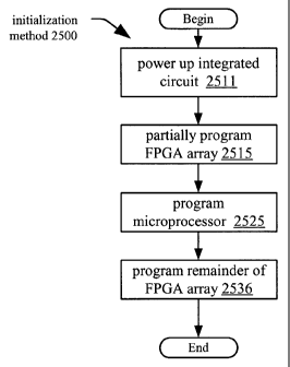
Figure 12 is a logic diagram illustrating an
embodiment of an initialization method 2500 performed in
accordance with certain aspects of the present invention.
In a block 2511, the integrated circuit is powered up.
Then, in a block 2515, the FPGA array is partially
configured. Subsequently, in a block 2525, the
microprocessor is programmed. In a block 2536, a remainder
of the FPGA array (that was not partially configured in the
block 2515) is then configured. This shows one of the
various embodiments shown within the Figure 12 for the
initialization method 2500.
Figure 13 is a logic diagram illustrating another
embodiment of an initialization method 2700 performed in
accordance with certain aspects of the present invention.
Initially, in a block 2710, the integrated circuit is
powered up. Then in a block 2711, one or more portion(s) of
an FPGA array are set up to provide access to a
microprocessor. This may be viewed as being performed to
gain access to the microprocessor input/output
functionality. Then, in a block 2713, the microprocessor
is booted. In a block 2731, the remainder of the FPGA
array is configured using the microprocessor. This may be
viewed as directing the configuration of the remainder of
the FPGA array using the microprocessor in the block 2731.
In alternative embodiments, one or more portion(s) of
the FPGA array that were used to start up and boot the
microprocessor may be reclaimed as shown in an alternative
block 2751 before ending the initialization method 2700.
In addition, the microprocessor may be reset after the FPGA
array has been configured as shown in an alternative block
2761. To perform this reset of the microprocessor after
the FPGA array has been configured, dedicated lines may be
used to perform the reset of the microprocessor as shown in
16
CA 02472231 2004-06-30
WO 03/061128 PCT/US02/41227
an alternative block 2762. Moreover, portions of the FPGA
array may be used themselves to control the reset of the
microprocessor. In addition, communicatively coupling via
block RAM may also be used to perform the reset of the
microprocessor as well.
Figure 14 is a logic diagram illustrating another
embodiment of an initialization method 2800 performed in
accordance with certain aspects of the present invention.
In a block 2810, the integrated circuit is powered up. In a
block 2811, a microprocessor is booted. This booting of
the block 2811 is performed using dedicated access to the
microprocessor in the Figure 14. Then, the FPGA array is
configured in the block 2822.
In addition, the microprocessor may be reset after the
FPGA array has been configured as shown in an alternative
block 2861. To perform this reset of the microprocessor
after the FPGA array has been configured, dedicated lines
may be used to perform the reset of the microprocessor as
shown in an alternative block 2862. Moreover, portions of
the FPGA array may be used themselves to control the reset
of the microprocessor. In addition, communicatively
coupling via block RAM may also be used to perform the
reset of the microprocessor as well.
Figure 15 is a logic diagram illustrating another
embodiment of an initialization method performed in
accordance with certain aspects of the present invention.
In a block 2902, the integrated circuit is powered up. In a
block 2905, one or more portion(s) of an FPGA array that
are near a microprocessor are configured using dedicated
access to the FPGA portion(s). Some of the FPGA portion(s)
may also include block RAM as shown in an alternative block
2906. Then, in a block 2911, the microprocessor is booted
using the configured portion(s) of the FPGA array.
In a block 2922, the FPGA array is configured. This
may be viewed as performing the remaining configuration of
the FPGA array. In alternative embodiments, one or more
portion(s) of the FPGA array may be reclaimed as shown in
an alternative block 2951 before ending the initialization
method 2900. In addition, the microprocessor may be reset
17
CA 02472231 2004-06-30
WO 03/061128 PCT/US02/41227
after the FPGA array has been configured as shown in an
alternative block 2961. To perform this reset of the
microprocessor after the FPGA array has been configured,
dedicated lines may be used to perform the rest of the
microprocessor as shown in an alternative block 2962.
Moreover, portions of the FPGA array may be used themselves
to control the reset of the microprocessor. In addition,
communicatively coupling via block RAM may also be used to
perform the reset of the microprocessor as well.
In view of the above detailed description of the
invention and associated drawings, other modifications and
variations will now become apparent to those skilled in the
art. It should also be apparent that such other
modifications and variations may be effected without
departing from the spirit and scope of the invention.
18