Note: Descriptions are shown in the official language in which they were submitted.
CA 02472264 2004-07-02
WO 03/063954 PCT/US03/02435
CONDITIONING OF COUPLED ELECTROMAGNETIC
SIGNALS ON A LEAD
This application is a continuation-in-part of application Serial No.
10/059,598,
filed January 29, 2002.
This invention relates generally to implantable medical devices, and, more
particu-
lady, to a method and apparatus for trapping and/or conditioning
electromagnetic
phenomenon resulting from electromagnetic fields experienced by a medical
device lead.
The technology explosion in the implantable medical devices industry has
resulted
in many new and innovative devices and methods for analyzing and improving the
health
of a patient. The class of implantable medical devices now includes
pacemakers,
cardioverters, defibrillators, neuxal stimulators, and drug administering
devices, among
others. Today's state-of the-art implantable medical devices are vastly more
sophisticated
a
and complex than early ones, capable of performing significantly more complex
tasks.
The therapeutic benefits of such devices have been well proven.
There are many implementations of implantable medical devices that provide
'data
acquisition of important physiological data from a human body. Many
implantable
medical devices are used for cardiac monitoring and therapy. Often these
devices
comprise sensors that are placed in blood vessels and/or chambers of the
heart. Often
these devices are operatively coupled with implantable monitors and therapy
delivery
devices. For example, such cardiac systems include implantable heart monitoxs
and
therapy delivery devices, such as pace makers, cardioverter, defibrillators,
heart pumps,
cardiomyostimulators, ischernia treatment devices, drug delivery devices, and
other heart
therapy devices. Most of these cardiac systems include electrodes for sensing
and gain
amplifiers for recording and/or driving sense event signals from the inter-
cardiac or
remote electrogram (EGM).
Generally, a number of physiological data such as ventricular pressure, oxygen
supply in the patient's blood, EGM data, a patient's breathing patterns, and
the like, are
collected and stored by data acquisition devices implanted into a human body.
The data
can then be used to analyze the condition of a patient's physical state. Many
times,
information gathered by the implantable medical device may provide indications
of certain
conditions in a patient's body. Such conditions may affect the manner in which
medical
CA 02472264 2004-07-02
WO 03/063954 PCT/US03/02435
2
therapy (e.g., cardiac therapy) is delivered by the implantable medical
device. If a
particular condition is not detected properly, or a condition is misdiagnosed,
incorrect
reactions by the implantable medical device may occur. Incorrect reactions by
the
implantable medical device may cause harm to a patient. Generally,
physiological data
may be collected by a lead that delivers a signal relating to the
physiological data to
implantable medical device. In the presence of an electromagnetic field, the
signal on the
lead may become corrupted, causing errors.
Many times, delivery of therapy may be performed in response to certain
physiological data and/or data indicating other physical occurrences (e.g.,
unusual
breathing patterns) detected in a patient. For example, certain activities
performed by a
patient may lead to increased physiological indications in the patient's body.
Often, an
implantable medical device may be programmed to detect such physiological
changes and
react to them accordingly. For example, an implantable medical device may
deliver one
or more cardiac therapy in response to a particular condition detected in the
patient's body.
The implantable medical device may also modify the normal mode of therapy
delivery in a
patient's body in response to an unusual condition detected. Therefore,
improved
accuracy in the signal delivered by the lead is desirable for proper operation
of the
implantable medical device.
When an implantable medical device has been inserted into a patient's body, it
enters an area where the patient is exposed to a substantial amount of radio
frequency (RF)
signals. The length of the lead generally acts as an antenna during exposure
to radio
frequency signals, such as magnetic resonance imaging (MRI) processes and RF
signals
from radio diathermy processes. Due to the antenna-like behavior of the lead,
the tip of
the lead may behave as a source for the coupled (e.g., induced) current flow
created by the
RF signal. Furthermore, other portions of the lead, such as part that is
placed inside a
connector associated with the implantable medical device, may experience
coupled (e.g.,
induced) current flow created by the RF signal.
In the presence of MRI signals, (e.g., during MRI scanning processes), an
appreciable amount of current may be generated in the lead such that the tip
of the lead
contains a sizable magnitude of current gradient. Due to the conservation of
energy
principles, much of the current is converted to heat due to the energy loss
caused by the
CA 02472264 2004-07-02
WO 03/063954 PCT/US03/02435
resistance of the lead tip. Therefore, a significant amount of heat may be
generated at the
tip of the lead, which may cause serious bodily injury to a patient. Burns to
the tissue
exposed to the tip of the lead may occur. Furthermore, a large amount of
coupled current
in the lead may cause the implantable medical device to malfunction, thereby
creating a
risk of injury or death to the patient.
Changes to the signals traveling though the lead (e.g., sensor signals from
the lead
to the implantable medical device and/or therapy signals sent by the device)
may cause the
malfunctions in the operation of the implantable medical device. In such an
instance,
erroneous delivery of therapy may occur which may lead to heart arrhythmia or
other
physiological damage to a patient.
The present invention is directed to overcoming, or at least reducing the
effects of,
one or more of the problems set forth above.
SUMMARY OF THE INVENTION
In one aspect of the present invention, an apparatus is provided for reducing
I 5 coupled current resulting from an electromagnetic field in a medical
electrical lead. The
medical electrical lead comprises an elongate body having a proximal end
portion, a
middle portion, and a distal end portion and at least one coil wound about at
least one of
the proximal end portion, the middle portion, and the distal end portion, the
coil to provide
for filtering of radio frequency (RF) signal-coupled currents.
In another aspect of the present invention, a system is provided for reducing
coupled current resulting from an electromagnetic field in a medical
electrical lead. The
system of the present invention comprises an implantable medical device and a
medical
electrical lead operatively coupled to the implantable medical device. The
medical
electrical lead comprises a proximal end portion, a middle portion, and a
distal end portion
and at least one coil wound about at least one of the proximal end portion,
the middle
portion, and the distal end portion. The coil provides an inductive impedance
in parallel
with a capacitive impedance for reducing coupled currents resulting in the
presence of an
electromagnetic field.
In yet another aspect of the present invention, a method is provided for
reducing
coupled current resulting from an electromagnetic field in a medical
electrical Lead. The
method comprising providing at least one wound coil around at least one of a
proximate
CA 02472264 2004-07-02
WO 03/063954 PCT/US03/02435
4
end portion, a middle portion, and a distal end portion of the medical
electrical lead such
that the coil provides an inductive impedance in parallel with a capacitive
impedance to
reduce the coupled current.
BRIEF DESCRIPTION OF THE DRAWINGS
The inventions may be understood by reference to the following description
taken
in conjunction with the accompanying drawings, in which like reference
numerals identify
like elements, and in which:
Figure 1 is a simplified diagram of an implementation of an implantable
medical
device, in accordance with one illustrative embodiment of the present
invention;
Figure 2 illustrates a simplified block diagram representation of an
implantable
medical system in accordance with one illustrative embodiment of the present
invention;
Figure 3 illustrates a stylized depiction of a lead used in the implantable
medical
system, in accordance with one embodiment of the present invention;
Figure 4 illustrates a stylized depiction of the distal end of the lead used
in the
implantable medical system, in accordance with one embodiment of the present
invention;
Figure 5 illustrates a stylized depiction of a coil implemented on the lead
used in
the implantable medical system, in accordance with one embodiment of the
present
invention;
Figure 6 illustrates stylized depiction of a cross-sectional view of the coil
implemented on the lead used in the implantable medical system, in accordance
with one
embodiment of the present invention; and
Figures 7a-7i illustrate equivalent electrical circuit-diagram representations
of the
various implementations of coils) placed on the lead used in the implantable
medical
system, in accordance with at least one embodiment of the present invention.
While the invention is susceptible to various modifications and alternative
forms,
specific embodiments thereof have been shown by way of example in the drawings
and
are herein described in detail. It should be understood, however, that the
description
herein of specific embodiments is not intended to Limit the invention to the
particular
forms disclosed, but on the contrary, the intention is to cover all
modifications,
equivalents, and alternatives falling within the spirit and scope of the
invention as defined
by the appended claims.
CA 02472264 2004-07-02
WO 03/063954 PCT/US03/02435
DETAILED DESCRIPTION OF SPECIFIC EMBODIMENTS
Illustrative embodiments of the invention are described below. In the interest
of
clarity, not all features of an actual implementation are described in this
specification. It
will of course be appreciated that in the development of any such actual
embodiment,
numerous implementation-specific decisions must be made to achieve the
developers'
specific goals, such as compliance with system-related and business-related
constraints,
which will vary from one implementation to another. Moreover, it will be
appreciated that
such a development effort might be complex and time-consuming, but would
nevertheless
be a routine undertaking for those of ordinary skill in the art having the
benefit of this
disclosure.
There are many discrete processes involving the operation of implantable
medical
devices (e.g., pacemakers, cardio defibrillators, and the like). The operation
of an
implantable medical device includes collecting, storing, and analyzing
physiological data
relating to a patient, and/or delivering therapy (e.g., cardiac therapy) to a
portion of a
patient's body. Often, these tasks are performed by an implantable medical
system, which
includes an implantable medical device. Based upon the analysis performed by
the
implantable medical system, one or more therapies may be delivered to a
particular
portion of a patient's body. One example of such a therapy is a cardiac
therapy, which is
delivered to a patient's heart. Interpretation of the physiological data
andlor data relating
to unusual activities in the patient's body is important in determining the
behavior (e.g.,
therapy deliver patterns, etc.) of the implantable medical device.
Embodiments of the present invention provide for reducing the coupled (e.g.,
induced) current in a lead caused by RF signals present around the lead.
Embodiments of
the present invention provide for inserting a coil proximate to the tip of the
lead to
substantially isolate the tip from the lead, thereby reducing the possibility
of inducement
of an undesirable amount of current coupled or induced by RF signals, on the
lead.
Embodiments of the present invention provide for attaching a coil proximate to
the tip of a
lead, wherein an inductor in series with the resistivity of the lead is
effectively created.
Embodiments of the present invention provide for a circuit whose effective
resonance
occurs at radio frequency signals such that an open circuit is created for
radio frequency
coupled current signals present on the lead. In other words, the coil provided
by
CA 02472264 2004-07-02
WO 03/063954 PCT/US03/02435
6
embodiments of the present invention provide an open circuit or high impedance
for high
frequency signals, at the same time providing a normal signal path for low
frequency
signals such as pacing signals or data acquisition signals.
Turning now to Figure 1, one embodiment of implementing an implantable
medical device into a human body is illustrated. A sensor/therapy delivery
device 210
(e.g., devices attached to leads 114) placed upon the heart 116 of the human
body 105 is
used to acquire and process physiological data. An implantable medical device
220
collects and processes a plurality of data acquired from the human body 105.
In one
embodiment, the implantable medical device 220 may be a pacemaker or a
defibrillator.
The data acquired by the implantable medical device 220 can be monitored by an
external
system, such as the access device 240 comprising a programming head 122, which
remotely communicates with the implantable medical device 220. The programming
head 122 is utilized in accordance with medical device programming systems
known to
those skilled in the art having the benefit of the present disclosure, for
facilitating two-way
communication between the pacemaker 220 and the access device 240.
In one embodiment, a plurality of access devices 240 can be employed to
collect a
plurality of data processed by the implantable medical device 220 in
accordance with
embodiments of the present invention. The pacemaker 220 is housed within a
hermetically sealed, biologically inert outer canister or housing 113, which
may itself be
conductive so as to serve as an electrode in the pacemaker 220 pacing/sensing
circuit. One
or more pacemaker sensors/leads, collectively identified with reference
numeral 114 in
Figure 1, are electrically coupled to the pacemaker 220 and extend into the
patient's
heart 116 via a vein 118. Disposed generally near a distal end of the leads
114 axe one or
more exposed conductive electrodes (sensor/therapy delivery unit 210) for
receiving
electrical cardiac signals or delivering electrical pacing stimuli to the
heart 116. The leads
114 may be implanted with their distal end situated in either the atrium or
ventricle of the
heart 116. In an alternative embodiment, the sensors 210, or the leads 114
associated with
the sensors 210, may be situated in a blood vessel on the heart 116 via a vein
118.
Turning now to Figure 2, a system 200, in accordance with one embodiment of
the
present invention, is illustrated. The system 200 comprises a sensor/therapy
delivery unit
2I0, an implantable medical device 220, and an access device 240. Embodiments
of the
CA 02472264 2004-07-02
WO 03/063954 PCT/US03/02435
7
present invention provide a plurality of physiological data and non-
physiological data
from the sensor/therapy delivery unit 210 to the implantable medical device
220, which
are then processed and stored in the implantable medical device 220. The
sensor/therapy
delivery unit 210 may comprise a plurality of sensors that are capable of
acquiring
physiological and non-physiological data. Based upon data from the sensors)
210 and
other factors, the implantable medical device 220 may deliver a therapy to a
portion of the
patient's body 105, via the sensor/therapy delivery unit 210. The access
device 240,
which may communicate to the device 220 via an interface 230 (e.g., an
interface internal
to the device 220), can be used reprogram and/or make modifications to the
operation of
the implantable medical device 220. In one embodiment, a lead 114 (described
below)
coupled to the implantable medical device 220 is used to house the sensors)
210 and/or
the therapy delivery electrodes.
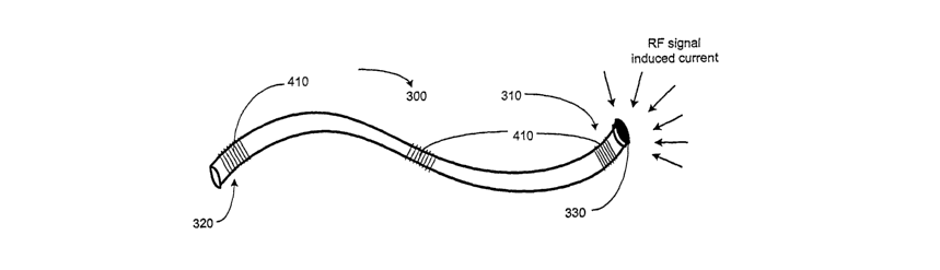
Turning now to Figure 3, a medical electrical lead 300, which may be coupled
to
the implantable medical device 220, is illustrated. The lead 300 may be
connected to an
implantable medical device 220 at approximately a proximal end portion 320 of
the lead
300. The lead 300 also comprises a middle portion 315, and a distal end
portion 310 at the
end of which is a tip 330. As illustrated in Figure 3, radio frequency (RF)
signal coupled
current present around the lead 300 may cause a current flow 340 in the lead
300. At the
tip 330, a RF signal source is effectively created due to the RF signals
present around the
lead 300.
In the presence of significant electro-magnetic fields, such as fields present
during
an MRI processes, a substantial amount of RF signal-coupled energy (e.g., a
current and/or
a voltage) may be present around the tip 330 of the lead 300. Therefore, the
large amount
of current 340 may be present at the tip 330, which causes an energy transfer
due to the
resistivity of the lead 300. Generally, the energy transfer due to the
resistivity of the lead
tip 330 to tissue interface is transferred in the form of heat. This causes
the tip 330 of the
lead 300 to become heated. The heat from the tip 330 of the lead 300 may then
be
transferred to the tissues surrounding the tip 330, causing harm to the
patient's body. The
electrical energy 340 generally occurs at the high RF frequencies, such as the
MRI
frequencies of 64 MHz and/or 128 MHz, or such as a radio diathermy frequency
27 MHz.
CA 02472264 2004-07-02
WO 03/063954 PCT/US03/02435
If the electrical energy 340 were effectively blocked, the heat generated at
the tip 330
would be substantially reduced.
Turning now to Figure 4, a coil 410 is attached to the lead 300 near the tip
330 of
the lead 300. In one embodiment, a plurality of coils 410 may be placed at
other portions
of the lead 300, such as at the proximate end portion 320 and/or at the middle
section/portion 315 of the lead 300, Placing the coil 410 at the distal end
310 of the lead
300 may prevent appreciable amounts of high frequency electrical energy 340
from
traveling through the extent of the length of the lead 300. Effectively, the
coil 410 acts as
an electromagnetic filter and/or trap, which are capable of trapping/filtering
RF signal-
electrical energy 340, such as electrical energy coupled by the presence of an
MRI signal.
Inductive and capacitive effects due to the implementation of the coil 410
(described in
greater detail below) reduce the flow of high-frequency currents 340 through
the tip 330 of
the lead 300. Therefore, heat generated due to the high-frequency current's
340
interaction with the resistivity of the lead tip 330 is reduced as a result of
the
implementation of the coil 410. Similarly, coils 410 placed at other portions
of the lead
also provide the benefit of reducing high-frequency currents 340 in the lead
tip 330.
Turning now to Figure 5, an enlarged view of the distal end 310 of the lead
300
and the coil 410, is illustrated. The coil 410 is wrapped around the lead 300
near the tip
330. The coil 410 provides the function of an inductor, whose inductive
properties at
higher signal frequencies, such as 64 and/or 128 MHz. As an example, the outer
diameter
of the spool of the coil 410 may be approximately 50 to 60 thousandths of an
inch. The
length of the coil 410 may be approximately one tenth to three tenths of an
inch. It should
be appreciated that other measurements may be implemented to achieve the
results taught
by embodiments of the present invention. The amount of windings of the coil
410 can be
varied to affect the capacitive and inductive effects created by the coil 410.
Therefore, the
windings of the coil 410 can be adjusted to provide capacitive and inductive
properties for
a variety of frequencies of currents resulting from electromagnetic fields.
These
capacitive and inductive properties may form a parallel inductor-capacitor
circuit network
that may be resonant.
In one embodiment, the coil 410 is made up of a wire that is insulated.
Turning
now to Figures 6a and 6b, a cross sectional view of a portion of the coil 410
and a 3-
CA 02472264 2004-07-02
WO 03/063954 PCT/US03/02435
9
dimensional view of a portion of the coil 410, respectively, are illustrated.
Tn one
embodiment, the wire within the coil 410 comprises conductive materials such
as copper,
gold, silver, MP35N, platinum, and the like. It should be appreciated that a
variety of
conductive materials 610 may be used in accordance with embodiments of the
present
invention. Furthermore, an insulated coating 640 that insulates the wire 610
is a dielectric
material, such as an enamel coating. The wire is wound about a dielectric (non-
conductive) core 630 and encapsulated by a dielectric outer shell 640. The
wire itself may
have an insulating coating as well. Due to the insulation of the coil 410, the
portion of the
lead 300 covered by the coil 410 is not electrically conducted to its
surrounding, therefore,
it does not function as an anode or an electrical return path of current into
the body of the
patient. However, the conductive material 610 of the coil 410 provides for
electrical
characteristics within the electrical path of the lead 300. Tn other words,
the conductive
material 610 of the coil 410 adds capacitive and/or inductive characteristics
to the
electrical path of the lead 300 in a series fashion.
Turning now to Figures 7A- 7I, equivalent electrical circuits that result from
various implementations of the coil 410 onto the lead 300, are illustrated. In
one
embodiment, the coil 410 provides an equivalent inductance in series with the
electrical
flow path of the lead 300, as illustrated in Figure 7A. The coil 410 provides
an inductor L
710 in series with an equivalent resistance R 720 (which in one embodiment is
the
equivalent resistance of the coil 410) in the electrical path of the lead 300,
which
terminates at the ring tip 330. Furthermore, the circuit in Figure 7A also
comprises an
equivalent resistance (RWtre 721) of the lead-wire itself. The inductor L 710
becomes
effective during the presence of an RF signal, such as an MRI signal of 64 MHz
and/or
12~ MHz. It should be appreciated the frequency at which the inductor L 710
becomes
effective may be modified by changing the winding of the coil 410 and remain
within the
spirit of embodiments of the present invention.
At low frequencies, such as a signal delivering a pacing signal to the tip 330
of the
lead 300, the inductance L 710 is an equivalent electrical-short within the
lead 300. As RF
signal frequency signals surround the lead 300, the inductor L 710 provides an
inductance
of various measurements, depending on the windings and/or the size of the
conductive
material 610 of the wire associated with the coil 410. In one embodiment, the
inductor L
CA 02472264 2004-07-02
WO 03/063954 PCT/US03/02435
710 is approximately 4.7 micro Henries, which is effectively active during the
presence of
an MRI signal field. This electrical effect is also present in the presence of
radio
frequency signals. The 4.7 micro Henry inductor may reduce the instantaneous
build-up
of high-frequency currents coupled by significant electromagnetic fields, such
as fields
5 caused by an MRI process, but not limited to MRI processes.
The coil 410 is wound and designed such that the inductor L 710 created by the
coil 410 may be resonant with radio frequency signals such as 64 MHz and 128
MHz
signals. In an alternative embodiment, the coil 410 may provide a
substantially large
inductance without resonance. Therefore, at RF signal frequencies a large
amount of
10 impedance is present in the lead 300, thereby providing a large obstacle
for RF coupled
currents in the lead 300. Effectively, a high impedance circuit is cxeated at
the location of
the inductor L 710 (for high-frequency electrical energy) during the presence
of high
frequency signal. The high impedance near the tip 330 of the lead 300 provided
by the
coil 410 at high frequencies, causes most of the length of the lead 300 to be
ineffective for
inducement of signals caused by RF signals. At the same time, the coil 410
allows the
passage of low frequency signals utilized by the implantable medical device
220. The
inductive reactance provided by the inductor L 710 significantly isolates high
frequency
(radio frequency) coupled signals in the lead 300 from the lead tip 330.
Turning now to Figure 7B, an alternative embodiment of the equivalent circuit
provided by the coil 410 at the tip 330 of the lead 300 is illustrated. The
coil 410 may be
wound in such a manner around the lead 300 that a capacitance C 730 is also
created. The
capacitance C 730 exists in parallel across the inductor L 710. The
capacitance C 730 is in
parallel with the inductor L 710 and the resistance R 720, which are in series
with
equivalent of the coil 410 and RWtre 721. The capacitance C 730 is generally
due to the
parasitic capacitance that is formed across each of the windings of the coil
410. Generally,
the capacitance C 730 is effective during the presence of high-frequency
signals at the tip
330 of the lead 300. The capacitance C 730 generally does not interfere with
low-
frequency signals on the lead 300, such as pacing signals sent by the
implantable medical
device 220 and/or physiological sensor signals traveling to the device 220.
The capacitance C 730 represents an equivalent capacitance of a combination of
the plurality of parasitic capacitance across the windings of the coil 410.
The combination
CA 02472264 2004-07-02
WO 03/063954 PCT/US03/02435
11
of the parallel configuration of the inductor L 710 and the capacitor C 730
provides a
parallel circuit that is of a higher impedance than the inductor L 710 by
itself. Therefore,
the circuit provided by the coil 410 provides for a broader range of
frequencies in which
significant high impedance at high frequencies is created near the tip 330 of
the lead 300.
In one embodiment, the inductor L 710 and the capacitor C 730 provides a self
resonant circuitry that reacts various RF signals, particularly to 27 MHz, 64
MHz, and/or
to 128 MHz signals. The resonance causes a high impedance at the RF signals,
such that
electrical energy coupled by the RF signals are significantly isolated. The
isolation of the
high frequency electrical energy provides the benefit of reducing of heating
at the tip 330
of the lead 300. By changing the diameter of the conductive material (wire)
610 in the
coil 410 and/or changing the number of windings of the coil 410, the self
resonant
circuitry can be designed to react at a variety of predetermined range of high
frequency
signals. This principle can be used to adapt embodiments of the present
invention to
respond to changing frequency implementation of MRI processes.
As shown in Figure 7C, at low frequencies, the low-frequency current (hoW
~.e9) 740
flows through the lead 300 through the resistor RW;re 721 to the resistor R
720 (e.g.,
approximately 3 Ohms in one embodiment), which is the equivalent resistance of
the lead-
wire and of the coil, respectively. In one embodiment, the equivalent
resistance of the
lead-wire RW;re 721 may be a small resistor of small value, such as a 35 Ohms
resistor.
Therefore, low-frequency signals, such as pacing signals and/or therapy
delivery signals,
can flow through the lead 300 and through the tip 330 to the tissue
surrounding the tip
330. In other words, the coil 410 does not interfere with normal operation of
therapy
delivery and/or physiological data collection performed by the implantable
medical device
220. However, at high frequencies, the inductor L 710 and/or the capacitance C
730
provide high impedance (see Figures 7C and 7D).
At high frequencies, the electrical energy coupled by RF signals that is
present at
the lead tip 330 is approximately zero due to the resonance nature of the
impedance
provided by the inductor L 710 and the capacitance C 730. At high frequencies,
a high
impedance is present as a result of the coil 410, substantially reducing the
value of the
electrical energy coupled by RF signals (Ih;gy, frea) at the lead tip 330.
Implementation of
one or more coils may produce a mufti-stage circuit illustrated in Figure 7E.
Figure 7E
CA 02472264 2004-07-02
WO 03/063954 PCT/US03/02435
12
illustrates two parallel sets of inductors and capacitors. The parallel
combination of
inductor Ll 726 (in series with R 720), both in parallel with capacitor C1 727
is in series
(through a second wixe resistance value RW;rea 721a) with the parallel
combination of
inductor LZ 728 (in series with a second equivalent resistance value R2 720a),
both in
parallel with capacitor C2 729, providing the high impedance effect at high
frequencies
illustrated in Figure 7D. The capacitors Cl 727 and CZ 729 may comprise lumped
elements) or parasitic capacitance. In one embodiment, each set of parallel
capacitor/inductor sets of Figure 7E may respond to a different frequency
signals, thereby
providing the high impedance benefits of Figure 7D at a plurality of
frequencies.
Implementation of the coils 410 as described by embodiments of the present
invention may be configuxed to produce an equivalent circuit illustrated in
Figure 7F.
Figure 7F illustrates a parallel combination of capacitor C3 733 and inductor
L3 731 in
series with inductor L4 732, all in parallel with capacitor C4 734, providing
a multi-
frequency response to provide a high-impedance obstacle for coupled high-
frequency
electrical energy. In one embodiment, inductor L3 731 may be a tapped inductor
and
capacitors C3 733 and C4 734 may be comprised of lumped elements.
A plurality of coils 410 may be implemented on the lead 300 to provide
protection
against coupled high-frequency electrical energy caused by a plurality of
signals of
different frequencies. For example two coils 410, one wound more loosely that
the other,
may be implemented on a lead 300. This would produce an equivalent circuit
that
comprises two different inductors, as illustrated in Figure 7G. Figure 7G
provides an
inductor LS 741 that is of a different value with a series inductor L6 742,
which results
from a coil 410 that is more tightly wound than the coil 410 that pxoduces the
inductor LS
741. Therefore, the respective inductors LS 741 and L6 742 can provide high-
impedance
obstacles to different coupled electrical energy resulting from two different
signals of
varying frequencies. The equivalent parasitic capacitance associated with each
coil 410 is
also different.
Figure 7H illustrates implementation of coils 410 on lead 300 connected to an
implantable medical device. The lead 300 is connected to a connector
module/block 750,
which is integrated with the implantable medical device 220. The connector
block 750
comprises a capacitor CS 752, which in one embodiment is a feed-through
capacitor. In
CA 02472264 2004-07-02
WO 03/063954 PCT/US03/02435
13
one embodiment, three coils 410 are implemented on the lead 300 to produce
three
inductors, L7 753, L$ 754, and L9 755. The inductor L7 7S3 is within the
connector block
750, and interacts with CS 752 to produce a low pass filter, which
substantially blocks
high-frequency signals and allows the flow of low-frequency signals to the
device 220.
The inductor L$ 754 acts as filter to break-up the resonant length of the lead
300. The
inductor L~ 755 provides protection against the induction of high-frequency
electrical
energy at the tip of the lead 300, as described above.
The concept of implementing the coil 410, as described in embodiments of the
present invention, may be extended by Winding a coil on a capacitor, as
illustrated in
Figure 7I. As illustrated in Figure 7I, a coil 410 is wound around a capacitor
762, which
may be implemented on a lead 300. This provides the ability to generate an
equivalent
circuit that more precisely responds to particular high-frequency signals. The
coil 410
wound around the capacitor 762 produces an parallel combination of a capacitor
C~ 764
and an inductor Lio 763, which can be used to provide a high impedance
obstacle to
coupled high frequency electrical energy with increased accuracy. The
capacitor C~ 764
and an inductor Llo 763 may be implemented onto a variety of portions of the
lead 300,
including the proximate end 320, the middle portion 315, and/or the distal end
310 of the
lead 300.
The equivalent circuits provided by Figures 7A-7I significantly reduce the
high
frequency electrical energy in the lead tip 330 due to exposure to radio
frequency signals,
such as MRI signals, diathermy signals, and a variety of other high-frequency
signals, or
output. The embodiments illustrated by Figures 7A-7I may be used individually
or in any
combination to produce high-impedance response called for by embodiments of
the
present invention.
The above detailed description is an illustrative example of an embodiment in
accordance with the present invention, of the implementation of the
implantable medical
device 220 described above. It should be appreciated that other
implementations and/or
embodiments can be employed within the spirit of the present invention. The
teachings
of the present invention can be utilized for a variety of systems relating to
electrical
circuitry, including cixcuitry that utilize stored charge.
CA 02472264 2004-07-02
WO 03/063954 PCT/US03/02435
14
The particular embodiments disclosed above are illustrative only, as the
invention
may be modified and practiced in different but equivalent manners apparent to
those
skilled in the art having the benefit of the teachings herein. Furthermore, no
limitations
are intended to the details of construction or design herein shown, other than
as described
in the claims below. Tt is therefore evident that the particular embodiments
disclosed
above may be altered or modified and all such variations are considered within
the scope
and spirit of the invention. Accordingly, the protection sought herein is set
forth in the
claims below.