Note: Descriptions are shown in the official language in which they were submitted.
CA 02472349 2004-07-05
WO 2004/001487 PCT/US2003/017299
REFLECTIVE SPATIAL LIGHT MODULATOR
BACKGROUND
s CROSS-REFERENCE TO RELATED APPLICATION
[0001] The present application claims priority from provisional U.S. Patent
Application
Serial No. 60/390,389, for "Reflective Spatial Light Modulator," filed June
19, 2002, the
disclosure of which is incorporated by reference.
FIELD OF THE INVENTION
to [0002] This invention relates to spatial light modulators (SLMs), and more
particularly to a
micro-mirror array with electronically addressable control circuitry for
display applications.
BACKGROUND OF THE INVENTION
[0003] Spatial light modulators (SLMs) have numerous applications in the areas
of optical
information processing, projection displays, video and graphics monitors,
televisions, and
Is electrophotographic printing. Reflective SLMs are devices that modulate
incident light in a
spatial pattern to reflect an image corresponding to an electrical or optical
input. The incident
light may be modulated in phase, intensity, polarization, or deflection
direction. A reflective
SLM is typically comprised of an area or two-dimensional array of addressable
picture
elements (pixels) capable of reflecting incident lights. Source pixel data is
first processed by
zo an associated control circuit, then loaded into the pixel array, one frame
at a time.
[0004] Prior art SLMs have various drawbacks. These drawbacks include: a lower
than
optimal optically active area (measured as what fraction of the device's
surface area that is
reflective, also called the "fill ratio") that reduces optical efficiency,
rough reflective surfaces
that reduce the reflectivity of the mirrors, diffraction that lowers the
contrast ratio of the
2s display, use of materials that have long-term reliability problems, and
complex manufacturing
processes that increase the expense of the product.
[0005] Many prior art devices include substantial non-reflective areas on
their surfaces.
This provides low fill ratios, and provides lower than optimum reflective
efficiency. For
example, U.S. Patent Number 4,229,732 discloses MOSFET devices that are formed
on the
CA 02472349 2004-07-05
WO 2004/001487 PCT/US2003/017299
surface of a device in addition to mirrors. These MOSFET devices take up
surface area,
reducing the fraction of the device area that is optically active and reducing
reflective
efficiency. The MOSFET devices on the surface of the device also diffract
incident light,
which lowers the contrast ratio of the display. Further, intense light
striking exposed
s MOSFET devices interfere with the proper operation of the devices, both by
charging the
MOSFET devices and overheating the circuitry.
[0006] Some SLM designs have rough surfaces, which also reduce reflective
efficiency.
For example, in some SLM designs the reflective surface is an aluminum film
deposited on an
LPCVD silicon nitride layer. It is difficult to control the smoothness of
these reflective mirror
ao surfaces as they are deposited thin films. Thus, the final product has
rough surfaces, which
reduce the reflective efficiency.
[0007] Another problem that reduces reflective efficiency with some SLM
designs,
particularly in some top hanging mirror designs, is large exposed hinge
surface areas. These
large exposed hinge surface areas have to be blocked by a slab, typically made
of tungsten, on
Is top of the hinge to prevent the scattering of incident light. These slabs
significantly reduce the
optically active area and lower the reflective efficiency.
[0008] Many conventional SLMs, such as the SLM disclosed in U.S. Patent Number
4,566,935, have hinges made of aluminum alloy. Aluminum, as well as other
metals, is
susceptible to fatigue and plastic deformation, which can lead to long-term
reliability
2o problems. Also, aluminum is susceptible to cell "memory", where the rest
position begins to
tilt towards its most frequently occupied position. Further, the mirrors
disclosed in the
4,566,935 patent are released by undercutting the mirror surface. This
technique often results
in breakage of the delicate micro-mirror structures during release. It also
requires large gaps
between mirrors, which reduce the fraction of the device area that is
optically active.
2s [0009] What is desired is an SLM with improved reflective efficiency, SLM
device long-
term reliability, and simplified manufacturing processes.
SUMMARY OF THE INVENTION
[0010] The present invention is a spatial light modulator (SLM). In one
embodiment, the
SLM~has a reflective selectively deflectable micro mirror array fabricated
from a first substrate
3o bonded to a second substrate having individually addressable electrodes.
The second substrate
may also have addressing and control circuitry for the micro mirror array.
Alternatively,
portions of the addressing and control circuitry are on a separate substrate
and connected to the ,
circuitry and electrodes on the second substrate.
2
CA 02472349 2004-07-05
WO 2004/001487 PCT/US2003/017299
[0011] The micro mirror array includes a controllably deflectable mirror plate
with a
reflective surface to reflect incident light. The mirror plate is connected to
a vertical hinge by
a connector, and the hinge is in turn connected to spacer walls by support
posts. Each of the
mirror plate, the connector, the vertical hinge, the support posts, and the
spacer walls is
s fabricated from a first substrate. This first substrate is a wafer of a
single material, single
crystal silicon in one embodiment. The spacer walls provide separation between
the mirror
plate and an electrode associated with that mirror plate that controls the
deflection of the
mirror plate, and is located on the second substrate bonded to the micro
mirror array. The
close spacing of the mirror plates and the vertical orientation of the hinge
allow the reflective
to surfaces to have a very high fill ratio for the micro mirror array. Very
little light gets past the
micro mirror array to strike the circuitry on the second substrate.
[0012] The spatial light modulator is fabricated with few steps, which keeps
the fabrication
cost and complexity low. Cavities are formed in a first side of the first
substrate. This is done
in a single anisotropic etch in one embodiment. In parallel, the electrodes
and addressing and
as control circuitry are fabricated on a first side of the second substrate.
The first side of the first
substrate is bonded to the first side of the second substrate. The sides are
aligned so the
electrodes on the second substrate are in proper relation with the mirror
plates which the
electrodes will control. The second side of the first substrate is thinned to
the desired
thickness. Optionally, a layer of reflective material may be deposited on a
second side of the
2o first substrate. A second anisotropic etch defines the support posts, the
vertical hinges, and the
connectors, and releases the mirror plates from the second side of the first
substrate. Thus, the
spatial light modulator may be fabricated by only two main etch steps.
BRIEF DESCRIPTION OF THE DRAWINGS
[0013] Figure 1 is a diagram that illustrates the general architecture of a
spatial light
zs modulator according to one embodiment of the invention.
[0014] Figures 2,a and 2b are perspective views of a single micro mirror.
[0015] Figures 3a and 3b are perspective views showing the top and sides of a
micro
mirror array.
[0016] Figures 4a and 4b are perspective views showing the bottom and sides of
the micro
3o mirror array.
[0017] Figures Sa and Sb are top views of the micro mirror array.
[0018] Figures 6a and 6b are bottom views of the micro mirror array.
3
CA 02472349 2004-07-05
WO 2004/001487 PCT/US2003/017299
[0019] Figures 7a - 7d are perspective views showing the top, bottom, and
sides of a
single mirror of an alternate embodiment of the micro mirror array.
[0020] Figures 8a - 8d are perspective views showing the top and bottom of the
alternate
micro mirror array.
s [0021] Figure 9a is a flowchart illustrating a preferred embodiment of how
the spatial light
modulator is fabricated.
[0022] Figures 9b through 9j are block diagrams illustrating the fabrication
of the spatial
light modulator in more detail.
[0023] Figure 10 illustrates the generation of the mask and the etching that
forms the
~o cavities in the first substrate in more detail.
[0024] Figure 11 is a perspective view of one embodiment of the electrodes
formed on the
second substrate.
[0025] Figure 12 is a perspective view showing the micro mirror array on the
first
substrate positioned over the electrodes and other circuitry on the second
substrate.
Is [0026] Figure 13 illustrates a simplified embodiment of a mask that is used
in etching the
upper surface of the first substrate.
[0027] Figure 14 is a cross-section of a portion of the two substrates bonded
together.
DETAILED DESCRIPTION OF THE PREFERRED EMBODIMENTS
20 [0028] The reflective spatial light modulator ("SLM") 100 has an array 103
of deflectable
mirrors 202. Individual mirrors 202 can be selectively deflected by applying a
voltage bias
between that mirror and a corresponding electrode 126. The deflection of each
mirror 202
controls light reflected from a light source to a video display. Thus,
controlling the deflection
of a mirror 202 allows light striking that mirror 202 to be reflected in a
selected direction, and
zs thereby allows control of the appearance of a pixel in the video display.
Spatial Light Modulator Overview:
[0029] Figure 1 is a diagram that illustrates the general architecture of an
SLM 100
according to one embodiment of the invention. The illustrated embodiment has
three layers.
The first layer is a mirror array 103 that has a plurality of deflectable
micro mirrors 202. In
30 one preferred embodiment, the micro-mirror array 103 is fabricated from a
first substrate 105
that is a single material, such as single crystal silicon.
[0030] The second layer is an electrode array 104 with a plurality of
electrodes 126 for
controlling the micro-mirrors 202. Each electrode 126 is associated with a
micro-mirror 202
4
CA 02472349 2004-07-05
WO 2004/001487 PCT/US2003/017299
and controls the deflection of that micro-mirror 202. Addressing circuitry
allows selection of a
single electrode 126 for control of the particular micro-mirror 202 associated
with that
electrode 126.
[0031] The third layer is a layer of control circuitry 106. This control
circuitry 106 has
s addressing circuitry, which allows the control circuitry 106 to control a
voltage applied to
selected electrodes 126. This allows the control circuitry 106 to control the
deflections of the
mirrors 202 in the mirror array 103 via the electrodes 126. Typically, the
control circuitry 106
also includes a display control 108, line memory buffers 110, a pulse width
modulation array
112, and inputs for video signals 120 and graphics signals 122. A
microcontroller 114, optics
to control circuitry 116, and a flash memory 118 may be external components
connected to the
control circuitry 106, or rnay be included in the control circuitry 106 in
some embodiments. In
various embodiments, some of the above listed parts of the control circuitry
106 may be
absent, may be on a separate substrate and connected to the control circuitry
106, or other
additional components may be present as part of the control circuitry 106 or
connected to the
Is control circuitry 106.
[0032] In one embodiment, both the second layer 104 and the third layer 106
are fabricated
using semiconductor fabrication technology on a single second substrate 107.
That is, the
second layer 104 is not necessarily separate and above the third layer 106.
Rather, the term
"layer" is an aid for conceptualizing different parts of the spatial light
modulator 100. For
2o example, in one embodiment, both the second layer 104 of electrodes is
fabricated on top of
the third layer of control circuitry 106, both fabricated on a single second
substrate 107. That
is, the electrodes 126, as well as the display control 108, line memory
buffers 110, and the
pulse width modulation array 112 are all fabricated on a single substrate in
one embodiment.
Integration of several functional components of the control circuitry 106 on
the same substrate
2s provides an advantage of improved data transfer rate over conventional
spatial light
modulators, which have the display control 108, line memory buffers 110, and
the pulse width
modulation array 112 fabricated on a separate substrate. Further, fabricating
the second layer
of the electrode array 104 and the third layer of the control circuitry 106 on
a single substrate
107 provides the advantage of simple and cheap fabrication, and a compact
final product.
30 [0033] After the layers 103, 104, and 106 are fabricated, they are bonded
together to form
the SLM 100. The first layer with the mirror array 103 covers the second and
third layers 104,
106. The area under the mirrors 202 in the mirror array 103 determines how
much room there
is beneath the first layer 103 for the electrodes 126, and addressing and
control circuitry 106.
CA 02472349 2004-07-05
WO 2004/001487 PCT/US2003/017299
There is limited room beneath the micro mirrors 202 in the mirror array 103 to
fit the
electrodes 126 and the electronic components that form the display control
108, line memory
buffers 110, and the pulse width modulation array 112. The present invention
uses fabrication
techniques (described more fully below) that allow the creation of small
feature sizes, such as
processes that allow fabrication of features of 0.18 microns, and processes
that allow the
fabrication of features of 0.13 microns or smaller. Conventional spatial light
modulators are -
rnade through fabrication processes that do not allow such small features.
Typically,
conventional spatial light modulators are made through fabrication processes
that limit feature
size to approximately 1 micron or larger. Thus, the present invention allows
the fabrication of
to many more circuit devices, such as transistors, in the limited area beneath
the micro mirrors of
the mirror array 103. This allows integration of items such as the display
control 108, line
memory buffers 110, and the pulse width modulation array 112 on the same
substrate as the
electrodes 126. Including such control circuitry 106 on the same substrate 107
as the
electrodes 126 improves the performance of the SLM 100.
Is [0034] In other embodiments, various combinations of the electrodes 126 and
components
of the control circuitry may be fabricated on different substrates and
electrically connected.
The Mirror:
[0035] Figure 2a is a perspective view of a single micro mirror 202. In one
preferred
embodiment, the micro mirror 202 is fabricated from a wafer of a single
material, such as
2o single crystal silicon. Thus, the first substrate 105 in such an embodiment
is a wafer of single
crystal silicon. Fabricating the micro mirror 202 out of a single material
wafer greatly
simplifies the fabrication of the mirror 202. Further, single crystal silicon
can be polished to
create smooth mirror surfaces that have an order of magnitude smoother surface
roughness
than those of deposited films. Mirrors 202 fabricated from single crystal
silicon are
2s mechanically rigid, which prevents undesired bending or warping of the
mirror surface, and
hinges fabricated from single crystal silicon are durable, flexible, and
reliable. In other
embodiments, other materials may be used instead of single crystal silicon.
One possibility is "
the use of another type of silicon (e.g. polysilicon, or amorphous silicon)
for the micro mirror
202, or even making the mirror 202 completely out of a metal (e.g. an aluminum
alloy, or
3o tungsten alloy).
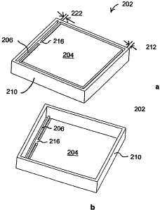
[0036] The micro mirror 202 has a top mirror plate 204. This mirror plate 204
is the
portion of the micro mirror 202 that is selectively deflected by applying a
voltage bias between
the mirror 202 and a corresponding electrode 126. In one embodiment this
reflective mirror
6
CA 02472349 2004-07-05
WO 2004/001487 PCT/US2003/017299
plate 204 is substantially square in shape, and approximately fifteen microns
by fifteen
microns, for an approximate area of 225 square microns, although other shapes
and sizes are
also possible. In one preferred embodiment, a large proportion of the surface
area of the micro
mirror array 103 is made up of the areas of the mirror plates 204 of the micro
mirrors 202.
s (003'7] The mirror plate 204 has a reflective surface that reflects light
from a light source at
an angle determined by the deflection of the mirror plate 204. This reflective
surface may be
the same material from which the micro mirror 202 is fabricated, in which case
the surface of
the mirror plate 204 is polished to a smoothness that provides the desired
level of reflectivity.
Alternatively, after fabrication of the micro-mirrors 202, a layer of
reflective material, such as
to aluminum, may be added to the surface of the mirror plate 204. Since in a
preferred
embodiment a large proportion of the surface area of the micro mirror array
103 is made up of
the areas of the mirror plates 204 of the micro mirrors, and the mirror plates
204 have
reflective surfaces, a large proportion of the surface area of the micro
mirror array 103 is
reflective and capable of reflecting light at a selected angle. Thus, the SLM
100 has a large fill
Is ratio, and efficiently reflects incident light.
[0038] The mirror plate 204 is connected to a torsion spring hinge 206 by a
connector 216.
The torsion spring hinge 206 is connected to a spacer support frame 210, which
holds the
torsion spring 206 in place. Note that other springs and connection schemes
between the
mirror plate 204, the hinge 206, and spacer support frame 210 could also be
used. The torsion
zo spring hinge 206 allows the mirror plate 204 to rotate relative to the
spacer support frame 210
about an 'axis between the walls of the spacer support frame 210 when a force
such as an
electrostatic force is applied to the mirror plate 204 by applying a voltage
between the mirror
202 and the corresponding electrode 126. This rotation produces the angular
deflection for
reflecting light in a selected direction. In one embodiment, this rotation
occurs about an axis '
zs that is substantially collinear with the long axis of the hinge. In one
preferred embodiment, the
torsion spring hinge 206 has a "vertical" alignment. That is, the hinge 206
has a width 222
that is smaller than the depth of the hinge (perpendicular to the mirror plate
204 surface). The
width of the hinge is typically between 0.1 microns to 0.5 microns, and is
approximately 0.2
microns in one embodiment. This "vertical" alignment of the hinge functions to
help
3o minimize non-reflective surfaces on the surface of the mirror array 103,
and keep the fill ratio
high. Also in one preferred embodiment, the
[0039] The spacer support frame 210 separates the mirror plate 204 from the
electrodes .
and addressing circuitry so that the mirror plate 204 may deflect downward
without contacting
7
CA 02472349 2004-07-05
WO 2004/001487 PCT/US2003/017299
the electrodes and other circuitry below. The spacer support frame 210
includes spacer walls
in one embodiment, which are typically not separate components from the rest
of the spacer
support frame 210. These walls help define the height of the spacer support
frame 210. The
height of the spacers 210 is chosen based on the desired separation between
the mirror plates
204 and the electrodes 126, and the topographic design of the electrodes. A
larger height
allows more deflection of the mirror plate 204, and a higher maximum
deflection angle. A
larger deflection angle provides a better contrast ratio. In one embodiment,
the maximum
deflection angle of the mirror plate 204 is 20 degrees. The spacer support
frame 210 also
provides support for the hinge 206 and spaces the mirror plate 204 from other
mirror plates
204 in the mirror array 103. The spacer support frame 210 has a spacer wall
width 212, which,
when added to a gap between the mirror plate 204 and the support frame 210, is
substantially
equal to the distance between adjacent mirror plates 204 of adjacent micro
mirrors 202. In one
embodiment, the spacer wall width 212 is 1 micron or less. In one preferred
embodiment, the
spacer wall width 212 is 0.5 microns or less. This places the mirror plates
204 closely together
is to increase the fill ratio of the mirror array 103.
[0040 In some embodiments, the micro mirror 202 includes elements that stop
the
deflection of the mirror plate 204 when the plate 204 has deflected downward
to a
predetermined angle. Typically, these elements include a motion stop and a
landing tip. When
the mirror surface 204 deflects, the motion stop on the mirror plate 204
contacts the landing
zo tip. When this occurs, the mirror plate 204 can deflect no further. There
are several possible
configurations for the motion stop and landing tip. In one embodiment, a
landing tip is
fabricated on the spacer frames 210 opposite to the hinge side. The maximum
tilt angle of
mirror plate 204 will be limited by the landing tip on the spacer frames 210
which stops the
downward mechanical motion of the mirror plate 204. Having a fixed maximum
tilt angle
zs simplifies controlling the spatial light modulator 100 to reflect incident
light in a known
direction.
[0041] In another embodiment, landing tips are fabricated along with the
electrodes 126 on
the second substrate 107. The landing tips of this embodiment may be
fabricated from an
insulator, such as silicon dioxide, to prevent a short circuit between the
mirror plate 204 and
3o the electrode 126. The maximum tilt angle of the mirror plate 204 is
limited in this
embodiment by the angle at which the mirror plate 204 contacts the landing tip
on the second
substrate 107. The height of the spacers 210 affects this angle; higher
spacers 210 allow larger
angles than lower ones. The landing tip on the second substrate 107 can be a
protruding bump,
CA 02472349 2004-07-05
WO 2004/001487 PCT/US2003/017299
which reduces the total surface area actually in contact. The bumps can be
held at the same
electrical potential as the mirror plate 204 to avoid welding on contact.
[0042] ~ In yet another embodiment, the gap between the mirror plate 204 and
the hinge 206
is accurately fabricated so when the mirror plate 204 tilts to a predetermined
angle, the corners
s of the plate 204 near the hinge 206 will contact the ends of the hinge 206,
which act as
mechanical stops. This occurs because the section of the hinge 206 connected
to the mirror
plate 204 deflects along with the mirror plate 204, but the sections of the
hinge 206 near the
support wall 210 remain relatively undeflected. For example, with a height of
the torsion
hinge 206 being 1 micron, a gap of 0.13 microns between the support wall and
the hinge 206
to will result in a maximum tilting angle of the mirror plate 204 of 15
degrees.
[0043] In one preferred embodiment, the motion stop and landing tip are both
made out of
the same material as the rest of the mirror 202, and are both fabricated out
of the first substrate
105. In embodiments where the material is single crystal silicon, the motion
stop and landing
tip are therefore made out of a hard material that has a long functional
lifetime, which allows
~s the mirror array 103 to last a long time. Further, because single crystal
silicon is a hard
material, the motion stop and landing tip can be fabricated with a small area
where the motion
stop contacts the landing tip, which greatly reduces sticking forces and
allows the mirror plate
204 to deflect freely. Also, this means that the motion stop and landing tip
remain at the same
electrical potential, which prevents sticking that would occur via welding and
charge injection
2o processes were the motion stop and landing tip at different electrical
potentials.
[0044] Figure 2b is a perspective view illustrating the underside of a single
micro mirror
202, including the support walls 210, the mirror plate 204, the hinge 206, and
the connector
216.
[0045] Figure 3a is a perspective view showing the top and-sides of a micro
mirror array
2s 103 having nine micro mirrors 202 -- 1 through 202 -- 9. While Figure 3a
shows the micro
mirror array 103 with three rows and three columns, for a total of nine micro
mirrors 202,
micro mirror arrays 103 of other sizes are also possible. Typically, each
micro mirror 202
corresponds to a pixel on a video display. Thus, larger arrays 103 with more
micro mirrors
202 provide a video display with more pixels. Since the hinges 206 in the
mirror array 103 all
3o face in parallel along one direction, light sources are directed at the
mirrors 202 in the array
103 along a single direction to be reflected to form a projected image on the
video display.
[0046] As shown in Figure 3a, the surface of the micro mirror array 103 has a
large fill
ratio. That is, most of the surface of the micro mirror array 103 is made up
of the reflective
9
CA 02472349 2004-07-05
WO 2004/001487 PCT/US2003/017299
surfaces of the mirror plates 204 of the micro mirrors 202. Very little of the
surface of the ,
micro mirror array 103 is nonreflective. As illustrated in Figure 3a, the
nonreflective portions
of the micro mirror array 103 surface are the areas between the reflective
surfaces of the micro
mirrors 202. For example, the width of the area between mirror 202-1 and 202-2
is determined
s by the spacer wall width 212 and the sum of the width of the gaps between
the mirror plates
204 of mirrors 202-1 and 202-2 and the support wall 210. The gaps and the
spacer wall width
212 can be made as small as the feature size supported by the fabrication
technique. Thus, in
one embodiment, the gaps are 0.2 micron, and in another embodiment the gaps
are 0.13
micron. As semiconductor fabrication techniques allow smaller features, the
size of the spacer
to wall 210 and the gaps can decrease to allow higher fill ratios. Figure 3b
is a perspective view
detailing one mirror 202 of the mirror array 103 of Figure 3a. Embodiments of
the present
invention allow fill ratios of 85%, 90%, or even higher.
[0047] Figure 4a is a perspective view showing the bottom and sides of the
micro mirror
array 103 shown in Figure 3. As shown in Figure 4a, the spacer support frames
210 of the
~s micro mirrors 202 define cavities beneath the mirror plates 204. These
cavities provide room
for the mirror plates 204 to deflect downwards, and also allow large areas
beneath the mirror
plates 204 for placement of the second layer 104 with the electrodes 126,
and/or the third layer ,
with the control circuitry 106. Figure 4b is a perspective view detailing one
mirror 202 of the
mirror array 103 of Figure 4a.
20 [0048] Figure Sa is a top view of the micro mirror array 103 having nine
micro mirrors 202
-- 1 through 202 -- 9 shown in Figures 3a and 4a. For example, for micro
mirror 202 -- l,
Figure Sa illustrates the mirror plate 204, the spacer support frame 210, the
torsion spring 206,
and the connector 216 connecting the mirror plate 204 to the torsion spring
206. Fig~lre Sa
also clearly illustrates, as described above with respect to Figure 3a, that
the micro mirror array
2s 103 has a large fill ratio. Most of the surface of the micro mirror array
103 is made up of the
reflective surfaces of the micro mirrors 202-1 through 202-9. Figure Sa
clearly illustrates how
fill ratio is determined by the areas of the reflective mirror plates 204 and
the areas between
the reflective surfaces of the mirror plates 204. The size of the areas
between the reflective
surfaces of the mirror plates 204 in one embodiment is limited by the feature
size limit of the
3o fabrication process. This determines how small the gaps between the mirror
plate 204 and the
spacer wall 210 can be made, and how thick the spacer wall 210 is. Note that,
while the
single mirror 202 as shown in Figure 2 has been described as having its own
spacer support
frame 210, there are not typically two separate abutting spacer walls 210
between mirrors such ,
CA 02472349 2004-07-05
WO 2004/001487 PCT/US2003/017299
as mirrors 202-1 and 202-2. Rather, there is typically one physical spacer
wall of the support
frame 210 between mirrors 202-1 and 202-2. Figure Sb is a perspective view
detailing one
mirror 202 of the mirror array 103 of Figure Sa.
[0049] Figure 6a is a bottom view of the micro mirror array 103 having nine
micro mirrors
s 202-1 through 202-9, as shown in Figures 3 through 5. Figure 6a shows the
bottom of the
mirror plates 204, as well as the bottoms of the spacer support frames 210,
the torsion springs
206, and the connectors 216. The area beneath the mirror plates 204 is large
enough in many
embodiments to allow the optimum design and placement of electrodes 126 and
control
circuitry 106, and space for accommodating a possible mirror landing tip.
Figure 6b is a
to perspective view detailing one mirror 202 of the mirror array 103 of Figure
6a
(0050] As seen in Figures Sa and 6a, very little light that is normal to the
mirror plate 204
can pass beyond the micro mirror array 103 to reach any the electrodes 126 or
control circuitry
106 beneath the micro mirror array 103. This is because the spacer support
frame 210, the
torsion spring 206, the connector 216, and the mirror plate 204 provide near
complete
Is coverage for the circuitry beneath the micro mirror array 103. Also, since
the spacer support
frame 210 separates the mirror plate 204 from the circuitry beneath the micro
mirror array 103,
light traveling at a non perpendicular angle to the mirror plate 204 and
passing beyond the
mirror plate 204 is likely to strike a wall of the spacer support frame 210
and not reach the
circuitry beneath the micro mirror array 103. Since little intense light
incident on the mirror
2o array 103 reaches the circuitry, the SLM 100 avoids problems associated
with intense light
striking the circuitry. These problems include the incident light heating up
the circuitry, and
the incident light photons charging circuitry elements, both of which can
cause the circuitry to
malfunction.
[0051] In Figures 3-6 each micro mirror 202 in the micro mirror array 103 has
its torsion
2s spring 206 on the same side. In one alternate embodiment, different micro
mirrors 202 in the
micro mirror array 103 have torsion springs 206 on different sides. For
example, returning to
Figure 3a, mirrors 202-1 and 202-3 would have springs 206 on the same side as
illustrated.
Mirror 202-2, in contrast, would have a spring 206 on a different side so that
the spring 206 of
mirror 202-2 is perpendicular to the springs 206 of mirrors 202-1 and 202-3.
This allows the .
3o mirror plates 204 of the different micro mirrors 202-1 and 202-2 to deflect
in different
directions, which gives the mirror array 103 as a whole more than one
controllable degree of
freedom. In this alternate embodiment, two different light sources (for
example, light sources
with differently colored light) can be directed toward the micro mirror array
103 and separately
11
CA 02472349 2004-07-05
WO 2004/001487 PCT/US2003/017299
selectively redirected by the micro mirrors 202 in the micro mirror array 103
form an image on
a video display. In such an embodiment, multiple micro mirrors 202 can be used
to reflect light
from the multiple light sources to the same pixel in the video display. For
example, two
different color light sources can be directed toward the mirror array 103
along different
s directions, and reflected by the array 103 to form a multicolor image on a
video display. The
micro mirrors 202-1 and 202-3 with torsion springs 206 on a first side control
the reflection of
a first light source to the video display. The micro mirrors such as micro
mirror 202-2 with
torsion springs 206 on a different second side control the reflection of a
second light source to
the video display.
to [0052] Figure 7a is a perspective view of a micro mirror 702 according to
an alternate
embodiment of the invention. The torsion hinge 206 in this embodiment is
diagonally oriented
with respect to the spacer support wall 210, and divides the mirror plate 204
into two parts, or
sides: a first side 704 and a second side 706. Two electrodes 126 are
associated with the
mirror 702, one electrode 126 for a first side 704 and one electrode 126 for a
second side 706.
~s This allows either side 704, 706 to be attracted to one of the electrodes
126 beneath and pivot
downward, and provides more total range of angular motion for the same support
wall 210
height as compared to the mirror illustrated in Figures 2-6. Figure 7b is a
more detailed view
of the mirror 702 and illustrates the mirror plate 204, hinge 206, and support
wall 210. Figures
7c and 7d illustrate the underside of a single mirror 702 and a more detailed
view of the
2o interior corner of the mirror 702. In other embodiments, the hinge 206 may
be substantially
parallel to one of the sides of the mirror plate 204, rather than diagonal,
and still be positioned
to divide the mirror plate 204 into two parts 704, 706.
[0053] Figures 8a through 8d are various perspective views of mirror arrays
composed of
multiple micro mirrors 702 as described in Figures 7a through 7d. Figures 8a
and 8b illustrate
2s the top of a mirror 702 array and a more detailed view of one mirror 702 in
the array. Figures
8c and 8d illustrate the underside of a mirror 702 array and a more detailed
view of one mirror
702 in the array.
Fabrication of the Spatial Light Modulator:
[0054] Figure 9a is a flowchart illustrating one preferred embodiment of how
the spatial
30 light modulator 100 is fabricated. Figures 9b through 9g are block diagrams
illustrating the
fabrication of the spatial light modulator 100 in more detail. In summary, the
micro mirrors
202 are partially fabricated on the first substrate 105. Separately, some or
all of the electrodes,
addressing circuitry, and control circuitry are fabricated on the second
substrate 107. The first
12
CA 02472349 2004-07-05
WO 2004/001487 PCT/US2003/017299
and second substrates 105 and 107 are then bonded together. The first
substrate 105 is
thinned, then lithography and etch steps follow. Then the fabrication of the
micro mirrors 202
is completed. Final steps, including packaging, complete the spatial light
modulator 100. In
one embodiment, the mirror array 103 is fabricated from a wafer of single
crystal silicon using
s only anisotropic dry etch methods, only two etches are done to fabricate the
mirror array 103,
and the circuitry is fabricated using standard CMOS techniques. This provides
an easy and
inexpensive way to fabricate the SLM 100.
[0055] Conventional spatial light modulators are fabricated with surface micro
machining
techniques that include etching, deposition of structural layers, deposition
and removal of
to sacrificial layers. These conventional MEMS fabrication techniques result
in poor yield, poor
uniformity, and result feature sizes of approximately 1 micron or larger. In
contrast, one
embodiment of the present invention uses semiconductor fabrication techniques,
which do not
include sacrificial layers, have much higher yields, and allow creation of
features of 0.13
microns or smaller. '
Is [0056] Referring to Figure 9a, a first mask is generated 902 to initially
partially fabricate
the micro mirrors 202. This mask defines what will be etched from one side of
the first
substrate 105 to form the cavities on the underside of the micro mirror array
103 that define the
spacer support frames 210 and support posts 208. Standard techniques, such as
photolithography, can be used to generate the mask on the first substrate. As
mentioned
zo previously, in one preferred embodiment the micro mirrors 202 are formed
from a single
material, such as single crystal silicon. Thus, in one preferred embodiment,
the first substrate
105 is a wafer of single crystal silicon. Note that typically multiple micro
mirror arrays 103, to
be used in multiple SLMs 100, are fabricated on a single wafer, to be
separated later. The
structures fabricated to create the micro mirror array 103 are typically
larger than the features
2s used in CMOS circuitry, so it is relatively easy to form the micro mirror
array 103 structures
using known techniques for fabricating CMOS circuitry. Figure 9b is a side
view that
illustrates the first substrate 105 prior to fabrication. The substrate 105
initially includes a
device layer 938, which is the material from which the mirror array 103 will
be fabricated, an
insulating oxide layer 936, and a handling substrate 934. Figure 9c is a side
view that
3o illustrates the first substrate 105 with the mask upon it.
[0057] After the mask is generated 902, in a preferred embodiment, the first
substrate 105
is anisotropically ion etched 904 to form the cavities beneath the mirror
plates 204. Put in .
another way, a "well" is formed in the first substrate for every micro mirror
202. Other
13
CA 02472349 2004-07-05
WO 2004/001487 PCT/US2003/017299
methods besides an anisotropic ion etch may also be used to form the cavities
or "wells," such
as a wet etch or a plasma etch. Figure 9d is a bloclc diagram that shows the
first substrate 105
with the cavities etched.
[0058] Separately from the fabrication of the cavities beneath the mirror
plates 204, the
s electrodes 126 and control circuitry 106 are fabricated 906 on the second
substrate 107. The
second substrate 107 may be a transparent material, such as quartz, or another
material. If the
second substrate is quartz, transistors may be made from polysilicon, as
compared to
crystalline silicon. The circuitry can be fabricated 906 using standard CMOS
fabrication
technology. For example, in one embodiment, the control circuitry 106
fabricated 906 on the
to second substrate 107 includes an array of memory cells, row address
circuitry, and column
data loading circuitry. There are many different methods to make electrical
circuitry that
perfoims the addressing function. The DRAM, SRAM, and latch devices commonly
known
may all perform the addressing function. Since the mirror plate 204 area may
be relatively
large on semiconductor scales (for example, the mirror plate 204 may have an
area of 225
1s square microns), complex circuitry can be manufactured beneath micro mirror
202. Possible
circuitry includes, but is not limited to, storage buffers to store time
sequential pixel
information, circuitry to compensate for possible non-uniformity of mirror
plate 204 to ,
electrode 126 separation distances by driving the electrodes 126 at varying
voltage levels, and
circuitry to perform pulse width modulation conversions.
20 [0059] This control circuitry 106 is covered with a passivation layer such
as silicon oxide
or silicon nitride. Next, a metallization layer is deposited. This
metallization layer is patterned
and etched to define electrodes 126, as well as a bias/reset bus in one
embodiment. The
electrodes 126 are placed during fabrication so that one or more of the
electrodes 126
corresponds to each micro mirror 202. As with the first substrate 105,
typically multiple sets
zs of circuitry to be used in multiple SLMs 100 are fabricated 906 on the
second substrate 107 to
be separated later.
[0060] Next, the first and second substrates are bonded 910 together. The side
of the first
substrate 105 that has the cavities is bonded to the side of the second
substrate 107 that has the
electrodes. The substrates 105 and 107 are aligned so that the electrodes on
the second
3o substrate 107 are in the proper position to control the deflection of the
micro mirrors 202 in the
micro mirror array 103. In one embodiment, the two substrates 105 and 107 are
optically
aligned using double focusing microscopes by aligning a pattern on the first
substrate 105 with
a pattern on the second substrate 107, and the two substrates 105 and 107 are
bonded together ,
14
CA 02472349 2004-07-05
WO 2004/001487 PCT/US2003/017299
by low temperature bonding methods such as anodic or eutectic bonding. There
are many
possible alternate embodiments to the fabrication 906. For example,
thermoplastics or
dielectric spin glass bonding materials can be used, so that the substrates
105 and 107 are
bonded thermal-mechanically. Figure 9e is a side view that shows the first and
second
s substrates 105, 107 bonded together.
[0061] After bonding the first and second substrates 105 and 107 together, the
surface of
the first substrate 105 that has not been etched is thinned 912 to a desired
thickness. First, the
handling substrate 934 is removed, as shown in Figure 9f, typically by
grinding or etching.
Then the oxide 936 is removed. Then, the device layer 938 is thinned or
polished, if
to necessary. This thinning is done in one embodiment by mechanical grinding
the substrate 105
to a thickness between the bottom of the fabricated "well" and the opposing
surface of the first
substrate 105 that is near the desired thickness of the micro mirror 202. In
one embodiment,
this thickness achieved by mechanical grinding is approximately 5 microns. The
substrate 105
is then polished by mechanical fine polishing or chemical mechanical polishing
to thickness
!s desired between the bottom of the "well" and the opposing surface of the
first substrate 105.
This thickness defines the thickness of the mirror plates 204. In one
embodiment, this desired
thickness is less than approximately 1 micron or less. Figure 9g is a side
view showing the
bonded first and second substrates 105, 107 after the first substrate 105 has
been thinned.
[0062] Next, the reflective surface of the micro mirror 202 is created. This
can be done
zo through polishing 913 the first substrate 105 so that the surface of the
first substrate 105 is
reflective. It is also possible to deposit 914 a layer of a reflective
material on the first substrate
105 to create a reflective surface. Other methods to create a reflective
surface may also be
used.
[0063] In one embodiment, a reflective layer of aluminum is deposited 914. The
thinned
2s surface of the first substrate 105 is coated with approximately 10 nm of
titanium seed thin
film. Then an approximately 30 nm thiclc layer of aluminum is deposited to
form a reflective
layer with a reflectivity above 95% over much of the visible optical spectrum.
Figure 9h is a
side view that shows a deposited reflective layer 932.
[0064] The reflective surface of the first substrate 105 is then masked and,
in a preferred
3o embodiment, high-aspect-ratio anisotropically ion etched 916 to finish
forming the micro
mirror array 103 and release the mirror plates 204. This second etch defines
the mirror plate
204, the torsion spring hinge 206, and the connector 216. Thus, it only takes
two etchings of
the first substrate 105 to fabricate the micro mirrors 202. This significantly
decreases the cost
CA 02472349 2004-07-05
WO 2004/001487 PCT/US2003/017299
of fabricating the micro mirrors 202. Figure 9i is a block diagram showing the
surface of the
first substrate 105 covered with the mask 933, and Figure 9j is a block
diagram showing the
spatial light modulator 100 after the second etching, including the mirror
plate 204, the hinge
206, the spacer support frame 210, and the electrode 126.
s [0065] In some embodiments, the hinges 206 are partially etched to be
recessed from the
surface of the mirror plates 204. Also, in some embodiments a reflective
surface is deposited
914 after the second etch that defines the mirror plate 204,~the torsion
spring hinge 206, arid
the connector 216. Such a reflective layer may be deposited by, for example,
evaporating
aluminum downwardly at an angle such that the horizontal vector of the angle
is from mirror
~o plate 204 to hinges 206. With this angle, and if the hinges 206 were etched
so that they are
recessed from the surface of the mirror plates 204, it is possible to deposit
substantially no
reflective coating on the surfaces of recessed hinges 206 to minimize the
optical scattering of
incident light by the surfaces of the torsion hinges 206. The evaporation may
occur, for
example, in the reaction chamber of an e-gun thermal evaporator at a
deposition rate of one
is nanometer per second.
[0066] In some embodiments, the micro-mirror array 103 is protected by a piece
of glass or
other transparent material. In one embodiment, during fabrication of the micro
mirror array
103, a rim is left around the perimeter of each micro mirror array 103
fabricated on the first
substrate 105. To protect the micro mirrors 202 in the micro mirror array 103,
a piece of glass
20 or other transparent material is bonded 918 to the rim. This transparent
material protects the
micro mirrors 202 from physical harm. In one alternative embodiment,
lithography is used to
produce an array of rims in a layer of photosensitive resin on a glass plate.
Then epoxy is
applied to the upper edge of the rims, and the glass plate is aligned and
attached to the
completed reflective SLM 100.
zs [0067] As discussed above, multiple spatial light modulators 100 may be
fabricated from
the two substrates 105 and 107; multiple micro mirror arrays 103 may be
fabricated in the first
substrate 105 and multiple sets of circuitry may be fabricated in the second
substrate 107.
Fabricating multiple SLMs 100 increases the e~ciency of the spatial light
modulator 100
fabrication process. However, if multiple SLMs 100 are fabricated at once,
they must be
3o separated into the individual SLMs 100. There are many ways to separate
each spatial light
modulator 100 and ready it for use. In a first method, each spatial light
modulator 100 is
simply die separated 920 from the rest of the SLMs 100 on the combined
substrates 105 and
16
CA 02472349 2004-07-05
WO 2004/001487 PCT/US2003/017299
107. Each separated spatial light modulator 100 is then packaged 922 using
standard
packaging techniques.
[0068] In a second method, a wafer-level-chip-scale packaging is carried out
to
encapsulate each SLM 100 into separate cavities and form electrical leads
before the SLMs
s 100 are separated. This further protects the reflective deflectable elements
and reduces the
packaging cost. In one embodiment of this method, the backside of the second
substrate 107 is
bonded 924 with solder bumps. The backside of the second substrate 107 is then
etched 926 to
expose metal connectors that were formed during fabrication of the circuitry
on the second
substrate 107. Next, conductive lines are deposited 92~ between the metal
connectors and the
1o solder bumps to electrically connect the two. Finally, the multiple SLMs
are die separated
930. '
[0069] Figure 10 illustrates the generation 902 of the mask 1000 and the
etching 904 that
forms the cavities in the first substrate in more detail. In a preferred
embodiment, the first
substrate is a wafer of single crystal silicon. Oxide is deposited and
patterned on the first
is substrate. This results in the pattern shown in Figure 10, where area 1004
is oxide that will
prevent the substrate beneath from being etched, and areas 1002 are areas of
exposed substrate. ,
The areas of exposed substrate 1002 will be etched to form the cavities. The
areas 1004 that
are not etched remain, and form the spacer support posts 20~ and the spacer
support frame
210.
20 [000] In one embodiment, the substrate is etched in a reactive ion etch
chamber flowing
with SF6, HBr, and oxygen gases at flow rates of 100 stem, 50 stem, and 10
stem
respectively. The operating pressure is in the range of 10 to 50 mTorr, the
bias power is 60 W,
and the source power is 300 W. In another embodiment, the substrate is etched
in a reactive
ion etch chamber flowing with C12, HBr, and oxygen gases at flow rates of 100
stem, 50 stem,
as and 10 stem respectively. In these embodiments, the etch processes stop
when the cavities are
about 3-4 microns deep. This depth is measured using in-situ etch depth
monitoring, such as
in-situ optical interferometer techniques, or by timing the etch rate. '
[0071] In another embodiment, the cavities are formed in the wafer by an
anisotropic
reactive ion etch process. The wafer is placed in a reaction chamber. SF6,
HBr, and oxygen
gases are introduced into the reaction chamber at a total flow rate of 100
stem, 50 stem, and
20 stem respectively. A bias power setting of 50 W and a source power of 1 SOW
are used at a
pressure of 50 mTorr for approximately 5 minutes. The wafers are then cooled
with a backside ,
helium gas flow of 20 stem at a pressure of 1 mTorr. In one preferred
embodiment, the etch
17
CA 02472349 2004-07-05
WO 2004/001487 PCT/US2003/017299
processes stop when the cavities are about 3-4 microns deep. This depth is
measured using in-
situ etch depth monitoring, such as in-situ optical interferometer techniques,
or by timing the
etch rate.
[0072] Figure 11 is a perspective view of one embodiment of the electrodes 126
formed on
s the second substrate 107. In this embodiment, each micro mirror 202 has a
corresponding
electrode 126. The electrodes 126 in this illustrated embodiment are
fabricated to be higher
than the rest of the circuitry on the second substrate 107. As shown in Figure
11, material on
the sides of the electrodes 126 slopes down from the electrodes' top surface
in a somewhat
pyramid shape. In other embodiments, the electrodes 126 are located on the
same level as the
to rest of the circuitry on the second substrate 107, rather than extending
above the circuitry. In
one embodiment of the invention, the electrodes 126 are individual aluminum
pads of
approximately 10x10 microns in size. These electrodes 126 are fabricated on
the surface of
the second substrate 107. The large surface area of the electrodes 126 in this
embodiment
results in relatively low addressing voltages required to pull the mirror
plate 204 down onto
is the mechanical stops, to cause the full pre-determined angular deflection
of the mirror plates
204.
[0073] Figure 12 is a perspective view showing the micro mirror array 103 on
the first
substrate 105 positioned over the electrodes 126 and other circuitry on the
second substrate
107. This illustrates the relative positions of the micro mirrors 202 in the
micro mirror array
20 103 and the electrodes prior to bonding 910 the first and second substrates
105 and 107
together. Note that, for illustrative purposes, the micro mirrors 202 in the
micro mirror array
103 are shown as completed micro mirrors 202. However, in a preferred
embodiment, as
described with respect to Figure 9a, only the cavities beneath the mirror
plates 204 in the first
substrate 105 would have been etched prior to bonding the first substrate 105
to the second
2s substrate 107. The mirror plate 204, hinges 206, and connectors 216 would
not be fabricated
yet. In embodiments where the electrodes 126 are located above the level of
the rest of the
circuitry and material on the side of the electrodes 126 slopes down, the
sloping material helps
correctly position the first substrate 105 on the second substrate 107. ,
[0074] Figure 13 illustrates a simplified embodiment of a mask that is used in
etching 916
3o the upper surface of the first substrate 105. In the etching 916 step,
areas 1302 are left exposed
and are etched to release the mirror plates 204 and form the torsion springs
206, the connectors
216, and the support posts 208. Other areas 1304 are covered with photoresist
material and are
not etched. These areas include the mirror plates 204 themselves and the
material that will
18
CA 02472349 2004-07-05
WO 2004/001487 PCT/US2003/017299
form the hinges 206. As shown in Figure 13, most of the surface of the mirror
array 103 is
reflective. The fabrication process only creates small nonreflective gaps that
separate the
mirror plates 204 from the support walls 210 and hinges 206.
[0075] The upper surface of the first substrate 105 is etched to release the
mirror plates
s 204 and form the hinges 206 after the upper surface of the first substrate
105 is masked. In
one embodiment, it is etched in a reactive ion etch chamber flowing with SF6,
HBr, and
oxygen gases at a flow rate of 100 sccm, 50 sccm, and 10 sccm respectively.
The operating
pressure is in the range of 10 to 50 mTorr, and the bias power of 60 W and a
source power 300
W. Since the etch depth is typically less than 1 micron, there are several
other fabrication
to processes can achieve the same goal. Another embodiment uses Cl2 and oxygen
gases at an
operating pressure of 10 mTorr to 50 mTorr with bias and source power settings
of the etching
reaction chamber of 50 W and 300 W, respectively, to achieve tight dimension
control. The
etch process is stopped at the desired depth (in one embodiment, about 5
microns deep) using
in-situ etch depth monitoring or by timing the etch rate.
I s Operation:
[0076] In operation, individual reflective elements are selectively deflected
and serve to
spatially modulate light that is incident to and reflected by the mirrors.
[0077] Figure 14 is a cross-section that shows the micro mirror 202 above an
electrode
126. In operation, a voltage is applied to an electrode 126 to control the
deflection of the
zo corresponding mirror plate 204 above the electrode 126. As shown in Figure
14, when a
voltage is applied to the electrode 126, the mirror plate 204 is attracted to
the electrode. This
causes the mirror plate 204 to rotate about the torsion spring 206. When the
voltage is
removed from the electrode 126, the hinge 206 causes the mirror plate 204 to
spring back
upward. Thus, light striking the mirror plate 204 is reflected in a direction
that can be
2s controlled by the application of voltage to the electrode.
[0078] One embodiment is operated as follows. Initiahy the mirror plate is
undeflected.
In this unbiased state, an incoming light beam, from a light source, obliquely
incident to SLM
100 is reflected by the flat mirror plates 204. The outgoing, reflected light
beam may be
received by, for example, an optical dump. The light reflected from the
undeflected mirror
3o plate 204 is not reflected to a video display.
[0079] When a voltage bias applied between the mirror plate 204 and the bottom
electrode
126, the mirror plate 204 is deflected due to electrostatic attraction.
Because of the design of
the hinge 206, the free end of the mirror plate 204 is deflected towards the
second substrate
19
CA 02472349 2004-07-05
WO 2004/001487 PCT/US2003/017299
107. Note that in one preferred embodiment substantially all the bending
occurs in the hinge
206 rather than the mirror plate 204. This may be accomplished in one
embodiment by
malting the hinge width 222 thin, and connecting the hinge 206 to the support
posts 208 only
on both ends. The deflection of the mirror plate 204 is limited by motion
stops, as described
s above. The full deflection of the mirror plate 204 deflects the outgoing
reflected light beam
into the imaging optics and to the video display.
[0080] When the mirror plate 204 deflects past the "snapping" or "pulling"
voltage
(approximately 12 volts in one embodiment), the restoring mechanical force or
torque of the
hinge 206 can no longer balance the electrostatic force or torque and the
mirror plate 204
"snaps" down toward the electrode 126 to achieve full deflection, limited only
by the motion
stops. To release the mirror plate 204 from its fully deflected position, the
voltage must be
lowered substantially below the snapping voltage to a releasing voltage (e.g.,
approximately
3.3 volts, in the embodiment where the snapping voltage is 5.0 volts). Thus,
the micro mirror
202 is an electromechanically bistable device. Given a specific voltage
between the releasing
Is voltage and the snapping voltage, there are two possible deflection angles
at which the mirror
plate 204 may be, depending on the history of mirror plate 204 deflection.
Therefore, the
mirror plate 204 deflection acts as a latch. These bistability and latching
properties exist since
the mechanical force required for deflection of the mirror plate 204 is
roughly linear with
respect to deflection angle, whereas the opposing electrostatic force is
inversely proportional to
2o the distance between the mirror plate 204 and the electrode 126.
[0081] Since the electrostatic force between the mirror plate 204 and the
electrode 126
depends on the total voltage between the mirror plate 204 and the electrode
126, a negative
voltage applied to a mirror plate 204 reduces the positive voltage needed to
be applied to the
electrode 126 to achieve a given deflection amount. Thus, applying a voltage
to a mirror array
zs 103 can reduce the voltage magnitude requirement of the electrodes 126.
This can be useful,
for example, because in some applications it is desirable to keep the maximum
voltage that
must be applied to the electrodes 126 below 12V because a SV switching
capability is more
common in the semiconductor industry. In addition, the amount of charge needed
to bias each
electrode 126 where a voltage is applied to a mirror array 103 is smaller than
the charge
3o needed in an embodiment in which the mirror array 103 is held at a ground
potential. Thus the
time required to correctly apply the proper voltage to the electrode 126 and
deflect the mirror
plate 204 is relatively fast.
CA 02472349 2004-07-05
WO 2004/001487 PCT/US2003/017299
[0082] Since the maximum deflection of the mirror plate 204 is fixed, the SLM
100 can be
operated in a digital manner if it is operated at voltages past the snapping
voltage. The
operation is essentially digital because the mirror plate 204 is either fully
deflected downward
by application of a voltage to the associated electrode 126 or is allowed to
spring upward, with
s no voltage applied to the associated electrode 126. A voltage that causes
the mirror plate 204
to fully deflect downward until stopped by the physical elements that stop the
deflection of the
mirror plate 204 is known as a "snapping" or "pulling" voltage. Thus, to
deflect the mirror
plate 204 fully downward, a voltage equal or greater to the snapping voltage
is applied to the
corresponding electrode 126. In video display applications, when the mirror
plate 204 is fully
to deflected downward, the incident light on that mirror plate 204 is
reflected to a corresponding
pixel on a video display. When the mirror plate 204 is allowed to spring
upward, the light is .
reflected in such a direction so that it does not strike the video display.
[0083] During such digital operation, it is not necessary to keep the full
snapping voltage
on an electrode 126 after an associated mirror plate 204 has been fully
deflected. During an
is "addressing stage," voltages for selected electrodes 126 that correspond to
the mirror plates
204 which should be fully deflected are set to levels required to deflect the
mirror plates 204.
After the mirror plates 204 in question have deflected due to the voltages on
electrodes 126,
the voltage required to hold the mirror plates 204 in the deflected position
is less than that
required for the actual deflection. This is because the gap between the
deflected mirror plate
20 204 and the addressing electrode 126 is smaller than when the mirror plate
204 is in the
process of being deflected. Therefore, in the "hold stage" after the
addressing stage the voltage
applied to the selected electrodes 126 can be reduced from its original
required level without '
substantially affecting the state of deflection of the mirror plates 204. One
advantage of
having a lower hold stage voltage is that nearby undeflected mirror plates 204
are subject to a
2s smaller electrostatic attractive force, and they therefore remain closer to
a zero-deflected
position. This improves the optical contrast ratio between the deflected
mirror plates 204 and
the undeflected mirror plates 204. .
[0084] With the appropriate choice of dimensions (in one embodiment, spacer
210
separation between the mirror plate 204 and the electrode 126 of 1 to 5
microns and hinge 206
3o thickness of 0.05 to 0.45 microns) and materials (such as single crystal
silicon (100)), a
reflective SLM 100 can be made to have an operating voltage of only a few
volts. The torsion
modulus of the hinge 206 made of single crystal silicon may be, for example,
5x101° Newton
per meter-squared per radium. The voltage at which the electrode 126 operates
to fully deflect
21
CA 02472349 2004-07-05
WO 2004/001487 PCT/US2003/017299
the associated mirror plate 204 can be made even lower by maintaining the
mirror plate 204 at
an appropriate voltage (a "negative bias"), rather than ground. This results
in a larger
deflection angle for a given voltage applied to an electrode 126. The maximum
negative bias
voltage is the releasing voltage, so when the addressing voltage reduced to
zero the mirror
s plate 204 can snap back to the undeflected position
[0085] It is also possible to control the mirror plate 204 deflections in a
more "analog"
manner. Voltages less than the "snapping voltage" are applied to deflect the
mirror plate 204
and control the direction in which the incident light is reflected.
Alternate Applications:
to [0086] Aside from video displays, the spatial light modulator 100 is also
useful in other
applications. One such application is in maskless photolithography, where the
spatial light
modulator 100 directs light to develop deposited photoresist. This removes the
need for a
mask. to correctly develop the photoresist in the desired pattern.
Is [0087] Although the invention has been particularly shown and described
with reference to
multiple embodiments, it will be understood by persons skilled in the relevant
art that various
changes in form and details can be made therein without departing from the
spirit and scope of .
the invention. For example, the mirror plates 204 may be deflected through
methods other
than electrostatic attraction as well. The mirror plates 204 may be deflected
using magnetic,
2o thermal, or piezo-electric actuation instead.
22