Note: Descriptions are shown in the official language in which they were submitted.
CA 02472662 2004-06-28
D 02-1-863 PATENT APPLICATION
LED Light Source Assembly
[0001 ] The Applicants hereby claim the benefit of their provisional
application,
Serial Number 60/371,015 filed April 9, 2002 for Snap Together Automotive LED
Lamp
Assembly; and serial number 60/490,493 filed July 28, 2003 for LED Light
Source
Assembly.
Technical Field
[0002] The invention relates to electric lamps and particularly to electric
lamps using
LED light sources. More particularly the invention is concerned with LED light
sources
supported on a heat conductive plate in a reflector type lighting assembly.
BackEround Art
[0003] LEDs offer both increased lamp life and electrical efficiency.
Presently they
have insufficient individual luminous output to replace most other lamp forms
(incandescent, tungsten halogen, fluorescent, and high intensity discharge).
LEDs can be
grouped together to accumulate sufficient light output to compete with some of
the other
light sources. Because the individual LEDs are necessarily spaced apart, the
grouped
structures can fail to provide an adequate cumulative intensity. They may also
produce
high heat concentrations that shorten LED life. Because LEDs need to be
individually
wired into the grouped structure, such assemblies can require tedious or
expensive
assembly. There is then a need for an LED lamp structure that is readily
manufactured,
that provides relatively good cumulative intensity and provides good heat
dissipation.
Disclosure of the Invention
[0004] A compact LED light source providing intensive LED positioning along
with
good thermal dissipation can be made with a heat conductive plate supporting a
plurality
of LEDs mounted in thermal contact with the plate. The plate further supports
electrical
circuitry providing an electrical connection to the LEDs. A heat conductive
stem
mechanically supports the plate and may provide an electrical conduction path
and a
thermal conduction path away from the LEDs.
-1-
CA 02472662 2004-06-28
D 02-1-863 PATENT APPLICATION
Brief Descriution of the Drawings
[0005] FIG. 1 shows schematic view of a plate supporting a plurality of LED
light sources coupled to stem with a heat sink.
[0006]FIG. 2 shows an alternative plate and stem supporting a plurality
of LED
light
sources.
[0007]FIG. 3 shows an alternative plate and stem supporting a plurality
of LED
light
sources.
[0008]FIG. 4 shows a plate supporting a plurality of LED light
sources
[0009]FIG. 5 shows an alternative plate supporting a plurality
of LED chips
sources
coupled
to a
support
stem.
[0010]FIG. 6 shows a plate for supporting a plurality of LED light
sources
[0011FIG. 7 shows a stem for supporting a plate.
]
[0012]FIG. 8 shows a bottom perspective view of the construction
of FIG. 3
[0013]FIG. 9 shows a cross sectional of an alternative LED lamp
assembly of
FIG.
8
[0014]FIG. 10 shows a bottom perspective view of the alternative
LED lamp
assembly
of
FIG.
9
[0015]FIG. 11 shows an exploded view of the LED lamp assembly of
FIGS. 8, 9
and
[0016]FIG. 12 shows a perspective view of the assembled lamp of
FIG. 11.
Best Mode for Carrying Out the Invention
[0017] A light source assembly may be formed from a heat conductive plate,
supporting a plurality of LEDs; and connecting electrical circuitry. A heat
conductive
stem to duct heat from the plate supports the plate. The stem may be further
supported on
a base.
[0018] FIG. 1 shows a schematic design of a simple plate 20 supporting a
plurality of
LED light sources 30 connected by circuit traces (electrical circuitry 40).
The LEDs 30
are mounted on circuitry pads 44. The preferred plate 20 may be formed from a
metal or
-2-
CA 02472662 2004-06-28
D 02-1-863 PATENT APPLICATION
circuit board material with an inner side 22 and an outer side 24 facing in a
forward
direction 26. The plate 20 is a substantially solid, heat conductive piece. It
is preferably
round to enable rotational processing during LED mounting and assembly. It is
a
convenient aspect of the circular plate structure, that the plate 20 may be
axially mounted
in a machine for indexed rotation to LED mounting stations. The plate 20 may
then be
populated with LEDs 30 by indexed rotations followed by robotic welding of an
LED
chip to the pad 44, followed by jump wire or similar welds between the pads
44, and the
LED chips. The plate, LEDs and circuitry may be similarly rotated through a
coating
material to preserve and protect the LEDs. It is understood that other plate
shapes may
be used. Coupling features may be included in the plate such as a soldier or
glue groove,
a threaded hole, or a through passage for a threaded coupling, and so on
enabling the
plate 20 to be joined to the supporting stem S0. Additionally the plate 20 may
include
electrical wire ways, or other electrical connection accommodating features to
enable the
LEDs and circuitry to be coupled on one or both sides in a convenient fashion.
The plate
20 may also include decorative or esthetic features, such as a dome or similar
shape with
a mirror, white, black or colored front surface.
[0019] The preferred plate 20 carries printed circuit traces 40. In the
preferred
embodiment the circuit traces link the LEDs 30 in a series circuit. The
circuit traces 40
may be formed in substantially known ways by laying down insulating,
conductive, and
protective layers as may be necessary in electrically conductive strips 42
connecting a
plurality of mounting pads 44. The mounting pads 44 may be structured to
support either
LED chips ("chip on board" structure) or LED packages (such as TOPLEDs). In
the
preferred embodiment, the electrical circuitry 40 is formed on one side of the
plate, and
more particularly the, inside surface 22. The trace lines 42 then link to the
series of pads
44 arranged in one or more rings around the center of the plate 20. It is
understood that
there may be more then one series of LEDs within the various circuitry
alternatives. For
example there may be a first ring and a second ring, or alternate LEDs may be
coupled in
a first group and a second group thereby enabling a low beam (one set of LEDs
illuminated) and a high beam (an alternative set or both sets of LEDs
illuminated), or
enables a white output and a separate colored (red, amber, etc.) output. It is
also possible
to tune the light beam in the circuitry lay out by segmenting .the rings into
subsets
enabling in right or left side illuminations that in combination with a
reflector provide for
-3-
CA 02472662 2004-06-28
D 02-1-863 PATENT APPLICATION
beams angled to the right or left that may be combined in adjustable ratios.
Similarly one
may tune the intensity of such beam angling. It is equally possible to
incorporate subsets
of LEDs on a single support for alternative functions such as a fog, signal,
warning,
colored and other illumination purposes. It is understood that individual pads
44 may be
separately located at chosen points on the plate 20 and the pads 44 wired
together by
jumper wires. The jump wire structure is considered less desirable, being more
costly to
completed and more prone to mechanical injury.
[0020) LEDs 30 are mounted on the pads 44 and finally coupled into the circuit
structure 40. It is common misnomer to apply the term "LED" to the typical
commodity
LED package comprising an LED chip, a reflector, and wire connections that are
then
enclosed in a plastic housing. These pre-assembled LED package units can be
less
thermally and optically efficient than individually mounted LED chips ("chip
on board").
A preferred aspect of the present design is to use a "chip on board"
construction, where
the LED chips are mounted directly on the support structure, enabling
relatively greater
heat removal, and greater light emission. The preferred general method is to
couple the
LED chip to a first conductive surface of a pad 44, and then connect a jumper
wired from
an exposed side of the LED chip to a second coupling point on that pad 44. The
pads
(and LEDs) are then chained together in a series circuit 40. The series
circuit 40 is a
preferred because failure of one LED causes the lamp to go out, forcing
replacement of
the whole failing structure. In contrast, a parallel circuit tolerates a
progressive failure of
individual LEDs that can be a deceptively dangerous reduction in total light
as successive
LEDs fail. Once the group of LED chips are mounted on their respective pads
("chip on
board") and wired together, the relevant portions, for example, the LED
bearing side of
the plate; or the whole assembly may be coated with a clear protective
coating, such as a
clear silicone or epoxy as is known in the art. The coating resists
penetration by moisture
and mechanically protects the LED chips and fine wires. The coating process
and
materials are known in the art. The plate 20 is mounted on a thermally
conductive stem
50 to conduct heat away form the plate. The stem 50 may be a hollow column
with an
exterior surface 52 formed to be reflective to enhance light output, or formed
to be
minimally reflective to enhance the system optics and limit uncontrolled light
projection
(glare) as may be preferred. The stem 50 is preferably in turn coupled to a
thermally
-4-
CA 02472662 2004-06-28
D 02-1-863 PATENT APPLICATION
conductive radiator, such as a heat conductive disk 60. Electrical connectors
38 may be
passed through the column 50 and disk 60 to be connected to the circuit 40 on
plate 20
[0021 ] FIG. 2 shows an alternative schematic view of a flat plate 220
supporting LED
chips 230 on pads 244 electrically coupled by circuit traces 240. The plate
220 is
mechanically coupled to a stem 250 with a curved reflective surface 252
designed to
direct light from the LEDs 230 sideways to other optical elements, such as a
reflector,
lens or light guide. The stem 250 includes a central passage for electrical
leads 238 to
couple with the circuit traces 240. In one embodiment the plate 220 was about
13
millimeters in diameter, and about 1.6 millimeters thick. Eight LEDs were
equally
distributed around the periphery of the lower side of the plate.
[0022] The stem 50, 250 may be a simple hollow tube formed by known techniques
to support the plate 20, 220. The preferred stem S0, 250 is structured to
conduct heat
from the plate 20, 220. A metal stem 50, 250 is preferred. The plate 20, 220
may be
welded, screwed, soldiered, glued, or similarly coupled to the forward or
distal end of the
stem 50, 250. The opposite end or base of the stem 50, 250 may be conveniently
formed
to couple to a base structure. In a vehicle context, a lamp is subject to
constant vibration.
The stem 50 should then be sufficiently stiff to prevent sway of the plate 20
during
normal operation. The preferred stem has an outer diameter about half the
diameter of
the plate. In the preferred embodiment the stem 50, 250 has a hollow center.
The
electrical connection leads 38, 238 may then be extended through the hollow
center of the
stem 50, 250. The exterior surface of the stem 50, 250 is exposed to the light
generated
by the LEDs 30, 230. The exterior surface 52, 252 of the stem should then be
appropriately designed optically. In one preferred embodiment the exterior
surface 52,
252 of the stem includes a mirror finish and is smoothly arced to direct light
towards an
associated optical system of a reflector and lens. Optical design is
considered to be in the
scope of skilled art given the preferred beam pattern, and similar design
choices and
requirements. In an alternatively preferred embodiment the stem is a straight,
narrow
column to minimize interception and reflection of light from the LEDs.
(0023) The preferred stem is mechanically coupled to a base, which may include
coupling features to join with a reflector or similar optical housing by known
methods.
In the preferred embodiment the base structure also includes heat-sinking
features. The
stem then provides a heat conductive path from the plate to the heat sinking
features. The
-S-
CA 02472662 2004-06-28
D 02-1-863 PATENT APPLICATION
plate 20 and the stem 50 should then have a sufficiently broad coupling to
enable good
heat flow from one to the other. Similarly the stem 50 should have an equally
or even
broader base to conduct heat from the stem.
[0024) The lamp assembly may be structured to be replaceable with respect to a
reflector or similar optical assembly. This generally requires a more
expensive socket to
enable correct positioning of the LED lamp assembly, exclusion of water and
dirt, and so
on while tolerating the removal and replacement of the standard lamp. Because
LEDs
can have a life of up to 100,000 hours, there may be no reason to enable lamp
replacement. The LED lamp assembly may then be designed as a standard
component
that is permanently installed in a selected one of many possible optical
housings
(reflector or lens system) with the expectation that if there were a failure,
the whole lamp
structure would be replaced. The cost of the socket is then reduced. The whole
lamp
assembly may be factory aimed, and sealed. The standard LED lamp assembly can
then
be used as a standard component with any number differing optical housing
systems.
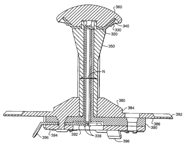
[0025) FIG. 3 shows an alternative plate and stem supporting a plurality of
LED light
sources. The plate 320 includes a series of peripheral petal like tabs 340
that are bent
upwards at an angle to the plane transverse to the stem axis. Each tab 340
supports an
LED assembly (package, or chip on board). Plate 320 is trapped between the
stem 350
and a heat conductive head 360. The coupling between the stem 350 and the head
360
may be a compression fit, bayonet mount or a similar construction. As shown,
the stem
350 end includes two semicircular pillars 370 that form a tight compression
fit with one
or more recesses formed in the head 360. The plate 320 is trapped in the
compression
between the stem 350 and the dome 360 enabling good thermal conduction from
the plate
320 and to the head 360 and stem 350. The plate 320 may be held in a recess
formed on
the top of the stem 350. Connecting electrical leads 338 may be extended
through the
stem 350 to the base assembly for electrical connection. The plate 320 may be
held in
place by compression, friction, potting, epoxy, or other methods. In one
embodiment, the
plate hade a thickness of about 1 millimeter. The plate had ten peripheral
tabs that were
conveniently bent at a 52 degree angle to the plane transverse to the stem
axis. The dome
had a diameter of about 20 millimeters. The dome to base distance was about 24
millimeters. The stem 350 was made of copper and had a middle height diameter
of
about 8 millimeters. The mating surface 384 had a diameter of about 21
millimeters.
-6-
CA 02472662 2004-06-28
D 02-1-863 PATENT APPLICATION
[0026] FIG. 4 shows a convenient layout of a stamped disk 400 with a crossbar
430
and two cut outs 440 that can mate with the two semicircular pillars 370. The
crossbar
430 is formed to align the disk 400 rotationally with the respect to the stem
350. The
radial edge of the disk 400 is formed with a plurality of radially extending
tabs or fingers
410 that support LED packages 420. The fingers 410 are angled with respect to
the stem
axis to point the LEDs 420 in a preferred direction, and correspondingly touch
the lower
(inside) surface of the head 360 for thermal conduction from the disk 400.
Appropriate
circuitry traces (not shown) may be laid out on the disk 400, fingers 410, and
cross bar
430 to electrically couple the LEDs 420 through the stem center. FIG. 5 shows
a similar
disk 500 with fingers 510 supporting a chip on board construction with LED
520. Again
the circuit traces are not shown. FIG. 6 shows a similar stamped disk 600. The
disk 600
may be made from a material with high thermal conductivity, such as copper.
The disk
600 may be stamped to have facets 610 to support circuitry and align
corresponding LED
packages or LED chips ("chip on board") as the case may be in a preferred
angle to the
lamp (stem) axis, while the center region 620 of the disk 600 is in thermally
conductive
contact with an associated stem and head if any.
[0027] Turning again to FIG. 3, the preferred stem 350 is supported in a
thermally
conductive disk or plate 380 that is exposed at least along its circumference
edge 382 to
air. The preferred plate 380 is cast or stamped metal, such as cast zinc or
stamped
copper, and may be blackened to enhance thermal radiation. The front side of
the plate
380 may include appropriate mating features 384 to guide or couple the lamp
assembly
into a lamp socket. The mating features 384 may be a threading, bayonet, clip
latching,
compression fit or other known latching features. In one embodiment the plate
380 had a
mating diameter (at 384) of 21 millimeters, and a peripheral diameter (at 382)
of about 36
millimeters.
[0028] The preferred plate 380 includes a back 386 abutting an electrically
insulating
portion 390 enclosing circuitry for the lamp supported on a circuit board 392.
A cover
394 may be attached to enclose the circuit board 392, allowing electrical
connectors to
protrude such as lug ends 396. FIG. 8 shows a bottom perspective view of the
construction of FIG. 3
[0029] The angle of the fingers, or of the bevel with respect to the stem can
then be
set in advance to influence the degree of light spread, or other optical
purposes.
_7_
CA 02472662 2004-06-28
D 02-1-863 PATENT APPLICATION
Interchangeable parts may then include stems of differing lengths, plates of
differing
radii, or circuitry, and fingers with differing angularity, and LEDs of
differing colors, all
of which may otherwise have standard assembly features. In this way a variety
of lamp
performances may be achieved from mixing and matching a limited number of
basic
parts that may otherwise be assembled in standard ways.
[0030] The forward (or top) surface of the plate may be enclosed with an
esthetic,
light or heat reflective shield, or heat dissipating plate or head 360. Such a
shield, cover
or head 360 may be attached to the plate by numerous known methods, including
press
fitting one or more extensions into one or more recesses.
[0031 ] In an alternative preferred embodiment, FIG. 9 shows a mushroom type
lamp
coupled to a heat sink-radiator. The head 910 and stem 920 of the mushroom are
made of
metal to conduct heat to the radiator 924. The LEDs 930 are mounted on a disk
940
under the rim of the cap 910 to direct light generally down toward the stem
920 and the
surrounding reflector 922. The LEDs 930 are mounted to the disk 920 so as to
conduct
heat to the cap 910, and stem 920 for conduction to the radiator 924. The
bottom side of
the radiator 924 is preferably formed with a cavity to retain a circuit board
950 for
controlling the LEDs 930. The circuit board 950 may be pressed in place or
similarly
mounted as may be convenient. A cover plate for the cavity may be used to
shield the
circuit board. In one embodiment the dome 910 had a diameter of about 20
millimeters,
and the stem had a wall thickness of about 3 millimeters.
[0032] The preferred alternative stem 920 is formed with a heat radiating
skirt 924 as
a single piece. The skirt 924 may include through passages so as to be screwed
or riveted
to the back of the reflector 922. Latching, snap, clip or similar coupling
features may be
formed on the skirt and reflector (or optical housing) to couple the two
pieces.
Conductive leads 960, 962 extend from the disk 940 through the stem 920 to the
circuit
board 950. Guiding and insulating the leads 960, 962 is or are one or more
electrically
insulating lead guides 964, 966 designed to funnel the leads through the stem
passage (or
passages) for exposure and connection of the distal (front end) of the stem
920. In the
preferred embodiment the stem center is funnel shaped and the lead guides 964,
966 are
conformally shaped conical sections. The lead ends project at each end of the
insulating
sheath so the contact may be made at the LED end and the circuit board end. It
is
convenient to form the core passage as a funnel or funnels and the insulative
sheath or
_g_
CA 02472662 2004-06-28
D 02-1-863 PATENT APPLICATION
sheath sections as cone that mate with the funnels. In this way the leads may
be easily
positioned correctly in the core of the stem.
[0033] FIG. 10 shows a bottom perspective view of the LED lamp assembly of
FIG.
9 having the heat radiating skirt 924 screwed by screws 970 to the back of the
reflector
922.
[0034] FIG. 11 shows the LED lamp assembly inserted axially through a rear
hole
formed in a reflector or housing with the cap 910 and stem 920 substantially
extending
above the surface of the reflector 922. The heat sink 924 may be mounted to
stand off
bosses 928 molded into the back of the reflector or housing using rivets or
screws for
example.
[0035] FIG. 12 shows a schematic view of the assembly sequence of the second
embodiment. The plate 920 with the attached LEDs 930 is formed in advance. The
circuit board 950 and cover plate if any are formed in advance. The leads 960,
962 are
attached to the circuit board 950. The insulating guides 964, 966 are threaded
over the
leads 960, 962. The circuit board assembly is pressed, riveted or screwed into
the cavity
formed in the back of the stem, so the leads end are exposed to the stem
front. The
preformed disk 940 carrying the LEDs 930 is then positioned on the stem end
and the
electrical connections to the leads 960, 962 completed. The rivet end 912 of
the dome
910 is then pressed through a hole in the disk 940 to mate with the distal end
of the stem
920, pinching the plate 940 in place and completing thermal conduction path
from the
plate 940. 'The lamp assembly is now complete. The dome end of the lamp may be
threaded through a reflector opening. Keyways, seals, and similar features
typical of
lamp to reflector couplings may be used as are known in the art. The lamp is
now
properly positioned with respect to the reflector. The skirt 924 as shown may
be screwed
to the back of the reflector 922.
[0036] The disk supporting the LEDs provides a convenient preassembly platform
enabling convenient manufacture. The close mounting of the LEDs provides
relatively
good intensity as a light source. Similarly the solid thermal coupling of the
disk to the
dome, stem and heat sink radiating skirt provides good thermal dissipation of
heat
generated by the concentrated array of LEDs. While there have been shown and
described what are at present considered to be the preferred embodiments of
the
invention, it will be apparent to those skilled in the art that various
changes and
-9-
CA 02472662 2004-06-28
D 02-1-863 PATENT APPLICATION
modifications can be made herein without departing from the scope of the
invention
defined by the appended claims.
- 10-