Note: Descriptions are shown in the official language in which they were submitted.
CA 02473222 2004-07-09
FP02-0336-00
DESCRIPTION
OPTICAL WAVEGUIDE MODULE
Technical Field
The present invention relates to an optical
waveguide module having an optical waveguide formed on
a substrate.
Background Art
In an optical circuit, which makes use of an
optical waveguide such as an optical fiber or planar
optical waveguide, it is sometimes desirable to control
the optical intensity of signal light to a suitable
value, such as keeping the optical intensity constant
for signal light transmitted through optical waveguides.
In such a case, the optical intensity of the signal
light is monitored in the optical circuit, and
sometimes the optical intensity is also controlled on
the basis of the results of this monitoring.
Disclosure of the Invention
This monitoring of the optical intensity of
signal light used to be accomplished by providing an
optical coupler on an optical waveguide and splitting
part of the signal light. With this method, an optical
coupler is provided at a specific location along the
optical waveguide, a few percent of the signal light is
split, and the optical intensity of the split light is
monitored with a photodetector, which allows the
1
CA 02473222 2004-07-09
FP02-0336-00
optical intensity of the signal light transmitted
through the optical waveguide to be monitored.
A problem with this use of an optical coupler,
though, is that it increases the number of optical
components that make up the optical circuit and
furthermore, since these have to be fused together, the
structure and the manufacturing process of the optical
circuit became more complicated.
In contrast, methods have been proposed in which
an optical coupler is not used, and instead part of the
signal light is reflected and the optical intensity is
monitored. With such a monitoring method, for example,
at a predetermined position of an optical waveguide in
a planar optical waveguide type optical circuit, part
of the signal light being transmitted through the
optical waveguide is reflected as the reflected light
for monitoring in the direction inclined at a
predetermined angle with respect to the optical axis.
And the reflected light is detected with a
photodetector disposed on the substrate on which the
optical waveguide is formed, whereby the signal light
is monitored.
However, in such monitoring method of the signal
light as described above, the reflected light is made
incident onto the light incident face of the
photodetector disposed on a substrate being inclined at
2
CA 02473222 2004-07-09
FP02-0336-00
an angle with respect thereto. Here, there occurs a
problem in that the photosensitivity for the reflected
light at the photodetector varies with polarization
states of the signal light, due to the polarization
dependence of the light, which passes through the light
incident face. In such case, the optical intensity of
the signal light cannot be monitored correctly unless
the polarization state of the signal light being
transmitted through the optical waveguide is identified.
The present invention has been accomplished in
order to solve the above problem, and it is an object
thereof to provide an optical waveguide module, with
which the optical intensity can be correctly monitored
regardless of the state of polarization of the signal
light.
In order to achieve the above object, an optical
waveguide module according to the present invention
comprises (1) an optical circuit, constituted by a
substrate and an optical waveguide formed on the
substrate and having a groove formed at a predetermined
inclination angle 8 (0°<A) with respect to the vertical
axis perpendicular to the optical axis of the optical
waveguide so as to cross a predetermined portion of the
optical waveguide, (2) a reflection filter that is
installed on the inside of the groove of the optical
circuit including a portion where signal light
3
CA 02473222 2004-07-09
FP02-0336-00
transmitted through the optical waveguide passes
through and that reflects part of the signal light
according to a specific reflectivity, and (3) a
photodetector that detects reflected light of the
signal light reflected by the reflection filter,
wherein (4) the photodetector is arranged such that the
reflected light is made incident onto the light
incident face thereof at a predetermined angle with
respect thereto.
With the above-mentioned optical waveguide module,
rather than the optical waveguide being split with an
optical coupler, part of the signal light is reflected
by a reflection filter, which is disposed in an
inclined groove provided to the optical waveguide, and
the optical intensity of the signal light can be
monitored by means of the reflected light. As a result,
the structure and manufacturing process of the optical
circuit are simplified.
Also, there is adopted a constitution made such
that the reflected light from the reflection filter is
made incident onto the light incident face of the
photodetector at a predetermined angle with respect
thereto. Here, since the polarization dependence of
the light, which passes through the light incident face,
is reduced, the photosensitivity for the reflected
light at the photodetector can be kept approximately
4
CA 02473222 2004-07-09
FP02-0336-00
constant regardless of the state of polarization of the
signal light. As a consequence, it is made possible to
monitor the optical intensity correctly regardless of
the state of polarization of the signal light.
As for the incident angle of the reflected light
with respect to the light incident face of the
photodetector, it is preferred to set the incident
angle, for example, to an angle, which is substantially
perpendicular to the Light incident face, or to an
IO angle within a predetermined range of angle including
90° and so on, in which the polarization dependence of
the light, which passes through the light incident face,
is sufficiently reduced. Further, as for the optical
waveguide provided in the optical circuit, for example,
an optical waveguide of planar optical waveguide type
formed on the substrate, or an optical fiber fixed onto
the substrate may be employed.
Brief Description of the Drawings
Fig. 1 is a plan view showing a structure of an
optical waveguide module in accordance with a first
embodiment.
Fig. 2 is a cross sectional view showing a
partially enlarged structure of cross section along the
optical axis of the optical waveguide module shown in
Fig. 1.
Fig. 3 is a cross sectional view showing the
5
CA 02473222 2004-07-09
FP02-0336-00
exemplary structure of the optical waveguide module.
Fig. 4A - Fig. 9C are graphs each showing the
polarization dependence of photosensitivity in
photodetectors.
Fig. 5A - Fig. 5C are graphs each showing the
polarization dependence of photosensitivity in
photodetectors.
Fig. 6A - Fig. 6C are graphs each showing a
change of light transmittance with respect to the film
thickness of an AR coat at light incident face.
Fig. 7A - Fig. 7C are graphs each showing a
change of light transmittance having polarization
dependence with respect to the film thickness of an AR
coat at light incident face.
Fig. 8 is a cross sectional view showing another
exemplary structure of the_optical waveguide module.
Fig. 9 is a plan view showing a structure of the
optical waveguide module in accordance with a second
embodiment.
Fig. 10 is a cross sectional view showing a
partially enlarged structure of cross section along the
optical axis of the optical waveguide module shown in
Fig. 9.
Fig. 11 is a plan view showing a structure of the
optical waveguide module in accordance with a third
embodiment.
6
CA 02473222 2004-07-09
FP02-0336-00
Fig. 12 is a cross sectional view showing a
partially enlarged structure of cross section along the
optical axis of the optical waveguide module shown in
Fig. 11.
Fig. 13 is a cross sectional view showing a
partially enlarged structure of cross section along the
optical axis of the optical waveguide module in
accordance with a fourth embodiment.
Fig. 14A and Fig. 14B are (A) a side view viewed
from the downstream side, and (B) a top view,
respectively, showing a structure of a sub-mounting
substrate and a photodetector array in the optical
waveguide module shown in Fig. 13.
Fig. 15A and Fig. 15B are cross sectional views
each showing a structure of cross section perpendicular
to the optical axis of an optical circuit; Fig. 15A
shows the case where an optical waveguide of planar
optical waveguide type is employed as the optical
waveguide, and Fig. 15B shows the case where an optical
fiber is employed as the optical waveguide.
Fig. 16 is a cross sectional view showing a
partially enlarged structure of cross section along the
optical axis of the optical waveguide module in
accordance with another embodiment.
Fig. 17A and Fig. 17B are (A) a top view and (B)
a side sectional view, respectively, showing an example
7
CA 02473222 2004-07-09
FP02-0336-00
of a first constitution of the photodetector array.
Fig. 18A and Fig. 18B are (A) a top view and (B)
a side sectional view, respectively, showing an example
of a second structure of the photodetector array.
Fig. 19A and Fig. 19B are (A) a top view and (B)
a side sectional view, respectively, showing an example
of a third structure of the photodetector array.
Best Mode for Carrying out the Invention
A preferred embodiment of an optical waveguide
module in accordance with the present invention will be
described below with reference to the drawings. In the
descriptions of drawings, the same elements will be
given with the same reference numerals and redundant
descriptions will be omitted. It is also noted that
dimensional ratios in the drawings do not always agree
with those in the description.
Fig. 1 is a plan view of a structure of an
optical waveguide module in accordance with a first
embodiment of the present invention. The optical
waveguide module comprises an optical circuit 1 which
are constituted of a substrate 10, and 8 optical
waveguides 21-2g (8 channels) disposed on the substrate
10. In this embodiment, for the optical waveguides 21-
28, an optical waveguide of planar optical waveguide
type, which are formed on the substrate 10, are
employed.
8
CA 02473222 2004-07-09
FP02-0336-00
Each of the optical waveguides 21-2$ is formed
parallel to each other at regular intervals along a
predetermined optical transmission direction (the
direction indicated by the arrowheads in Fig. 1) from
input end 11 toward output end 12 of a planar optical
waveguide type optical circuit 1. Also, at a
predetermined portion with respect to the optical
transmission direction of the planar optical waveguide
type optical circuit 1, a groove 3, which crosses the
optical waveguides 21-28, is formed.
Inside the groove 3, a reflection filter 4 for
reflecting part of signal light, which is transmitted
through each of the optical waveguides 21-28, with a
predetermined reflectance is provided. In this
embodiment, the inside of the groove 3 is sealed with
filler resin 5. Furthermore, at a position further
upstream than the groove 3, on the top side of the
planar optical waveguide type optical circuit 1, a sub-
mounting substrate 70 and a photodetector array 60 are
provided. The photodetector array 60 has 8
photodetectors 611-618 corresponding to each of the 8
optical waveguides 21-28 in the planar optical
waveguide type optical circuit 1.
In Fig. 1, with respect to the photodetectors
611-618, the shape of each light receiving surface is
represented by dotted line. Further, as for the sub-
9
CA 02473222 2004-07-09
FP02-0336-00
mounting substrate 70, to represent the structure of
the photodetector array 60, photodetectors 611-61~ and
the like, only the installation position thereof is
indicated by dot-dashed lines. Furthermore, the planar
optical waveguide type optical circuit 1 and the sub-
mounting substrate 70, or, the sub-mounting substrate
70 and the photodetector array 60 are fixed by means of,
for example, soldering.
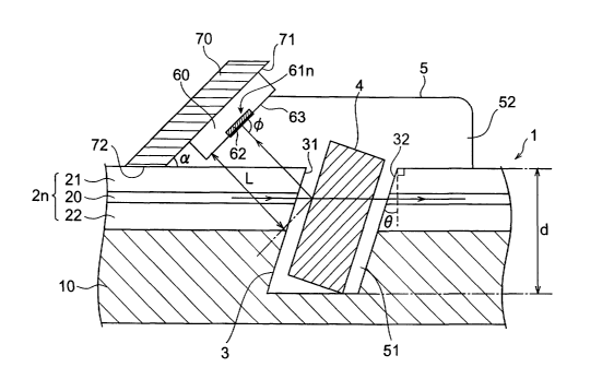
Fig. 2 is a cross sectional view showing a
structure of cross section of the optical waveguide
module shown in Fig. 1 along the direction of the
optical axis of the optical waveguides 2~ (n=1-8) (the
optical transmission direction of the planar optical
waveguide type optical circuit 1). In Fig. 2, a
portion, which includes the groove 3, the reflection
filter 4, and the photodetector array 60, is shown
enlarged.
As shown in Fig. 2, the optical waveguides 2" in
the planar optical waveguide type optical circuit 1 is
constituted of a lower clad 22, a core 20 and an upper
clad 21 being formed on the substrate 10. The groove 3,
that cuts across the optical waveguides 2n at a
predetermined portion, is formed obliquely at a
specific inclination angle 8 (0°<8) with respect to the
vertical axis perpendicular to the optical axis of the
optical waveguides 2~ (perpendicular to the substrate
CA 02473222 2004-07-09
FP02-0336-00
10) to a depth d including at least the portion, where
signal light transmitted through the optical waveguides
2~ passes through, corresponding to the core 20. In
this embodiment, the depth d of the groove 3 is set to
be greater than the thickness of the optical waveguides
2n up to the lower clad 22.
The reflection filter 4 is inserted on the inside
of the groove 3. The reflection filter 4 is installed
so as to include at least the portion where the signal
light transmitted through the optical waveguide 2"
passes through, at substantially the same angle 8, as
the groove 3 with respect to the optical axis. The
reflection filter 4 is preferably comprised of a
dielectric multi-layer film filter and is designed such
that part of the signal light with a predetermined
wavelength (within a predetermined wavelength band),
transmitted through the optical waveguides 2~ is
reflected with a specific reflectance.
Provided at the top side of the upper clad 21 of
the planar optical waveguide type optical circuit 1 is
the sub-mounting substrate 70. The sub-mounting
substrate 70 is a mounting member for mounting the
photodetector array 60, and one face thereof is a
photodetector mounting face 71 for mounting the
photodetector array 60 having the photodetectors 61"
(n=1-8) each corresponding to the optical waveguides 2".
11
CA 02473222 2004-07-09
FP02-0336-00
The photodetector array 60 is disposed on the
photodetector mounting face 71 such that each of the
reflected lights reflected by the reflection filter 4,
which are part of the signal light transmitted through
the optical waveguides 2~, is made incident onto a
light receiving portion 62 of the corresponding
photodetectors 61n.
The sub-mounting substrate 70 is fixed on the top
surface of the planar optical waveguide type optical
circuit 1 via a substrate fixing face 72, which is a
face adjacent to the photodetector mounting face 71.
Further, the substrate fixing face 72 is formed with an
angle larger than 90° with respect to the photodetector
mounting face 71. As a consequence, there is made an
arrangement such that the photodetector mounting face
71 is inclined at an angle a (0°<a,<90°) with respect to
the top surface of the planar optical waveguide type
optical circuit 1. The angle a. is determined by
referring to the light path of the reflected light from
the reflection filter 4.
In the example of structure shown in Fig. 2, for
the photodetectors 61n of the photodetector array 60, a
front-face incident type photodiode is used. The
surface of the photodetector array 60, in which the
light receiving portion 62 of the photodetectors 61n is
provided at the side opposite to the sub-mounting
12
CA 02473222 2004-07-09
FP02-0336-00
substrate 70, is the light incident face 63 for the
reflected light from the reflection filter 4.
As shown in Fig. 2, the angle a, formed by the
photodetector mounting face 71 and the top surface of
the planar optical waveguide type optical circuit 1 is
so set that the reflected light from the reflection
filter 4 is made incident onto the light incident face
63 of the photodetectors 61~ at a predetermined angle
with respect thereto (angle ~ shown in Fig. 2). Here,
there is made an arrangement such that the angle formed
by the light incident face 63 of the photodetector
array 60 and the top surface of the planar optical
waveguide type optical circuit 1 is the above-described
angle a..
Also, on the light incident face 63 of the
photodetectors 61~, an anti-reflection coat (AR coat),
which is a coat film for preventing the reflection of
the light within a predetermined wavelength band
corresponding to the wavelength band of the signal
light transmitted through the optical waveguides 2~, is
formed.
The inside of the groove 3 including the
reflection filter 4 is sealed with the filler resin 5.
The filler resin 5 in the present embodiment is
composed of an inner filler resin portion 51 sealing
the inside of the groove 3, and an upper filler resin
13
CA 02473222 2004-07-09
FP02-0336-00
portion 52 sealing a specific portion of the top
surface side of the planar optical waveguide type
optical circuit 1 including the upper portion of the
groove 3. These inner filler resin portion 51 and the
upper filler resin portion 52 are integrally formed
using the same resin material.
With the above-described structure, when the
signal light transmitted through an optical waveguide
2" is emitted via an upstream end face 31 to the inner
filler resin portion 51 inside the groove 3, the
reflection filter 4, which is inclined with respect the
optical axis, reflects part of the signal light
diagonally above the planar optical waveguide type
optical circuit 1 at a predetermined reflectance. The
rest of the signal light passes through the inner
filler resin portion 51 and reflection filter 4, and is
again made incident onto the optical waveguides 2,, via
a downstream end face 32.
Meanwhile, the light reflected by the reflection
filter 4, reaches the photodetector array 60 through
the inner filler resin portion 51, the optical
waveguides 2n and the upper filler resin portion 52,
and is made incident onto the photodetectors 61"
through the light incident face 63 at a predetermined
incident angle ~. Thus, the optical intensity of the
signal light transmitted through the optical waveguides
14
CA 02473222 2004-07-09
FP02-0336-00
2n is monitored based on the optical intensity of the
reflected light, detected by the light receiving
portion 62 of the photodetectors 61~.
Effects of the optical waveguide module in
accordance with the embodiment will be described below.
With the optical waveguide module shown in Fig. 1
and Fig. 2, rather than the optical waveguide itself
being split with an optical coupler, part of the signal
light is reflected by the reflection filter 4 disposed
in the inclined groove 3 formed on the optical
waveguides 2n, and the optical intensity of the signal
light can be monitored by means of the reflected light.
As a consequence, the structure and the manufacturing
process of the optical circuit are simplified.
Also, the following structure is adopted. That
is, the reflected light from the reflection filter 4 is
made incident onto the light incident face 63 of the
photodetectors 61~ of the photodetector array 60 at a
predetermined angle with respect thereto. Here, the
polarization dependence of the light passing through
the light incident face 63 is reduced. Accordingly, it
is possible to maintain the photosensitivity of the
reflected light at the photodetectors 61~ to a constant
level regardless of the polarization state of the
signal light. As a consequence, the optical intensity
can be monitored correctly regardless of the
CA 02473222 2004-07-09
FP02-0336-00
polarization state of the signal light.
Here, there is a need to set the incident angle
of the reflected light with respect to the light
incident face 63 of the photodetectors 61n to an angle
such that polarization dependence of the light passing
through the light incident face 63 is satisfactorily
reduced. To be more specific, for example, it is
preferred to set the angle to be substantially
perpendicular to the light incident face 63. Or, it is
preferred to set the angle within a predetermined range
of angle including 90°. As for the photodetector for
the photodetector array, a rear-face incident type
photodiode may be used. In this case, the light
receiving portion of the photodetector is formed on the
face opposite to the light incident face.
Further, in the optical waveguide module shown in
Fig. l, for the structure that the reflected light is
made incident onto the light incident face 63 of the
photodetectors 61" at a predetermined angle with
respect thereto, the following structure is adopted.
That is, the sub-mounting substrate 70, which is a
mounting member, is disposed on the top side of the
planar optical waveguide type optical circuit l; and
the photodetector array 60 including the photodetectors
61" is held by the photodetector mounting face 71,
which is inclined at an angle a (0°<oc<90°) with respect
16
CA 02473222 2004-07-09
FP02-0336-00
to the top surface of the planar optical waveguide type
optical circuit 1.
By adopting the above-described mounting member,
it is possible to place the photodetector array 60
including photodetectors 61~ in a positional state
being inclined with respect to the top surface of the
planar optical waveguide type optical circuit 1 in such
manner. That is, the light path of the reflected light,
which is emitted being inclined at a specific angle
with respect to the planar optical waveguide type
optical circuit l, and the light incident face 63 of
the photodetectors 61~ form the above-described
predetermined angle.
Further, in the optical waveguide module, a
plurality of channels is provided for the optical
waveguides 2n in the planar optical waveguide type
optical circuit 1 and for the corresponding
photodetectors 61n in the photodetector array 60. In
such structure as described above, when a problem of
cross talk arises between the adjacent channels, it is
preferred that, assuming that the distance between the
adjacent optical waveguides 2~ in the planar optical
waveguide type optical circuit 1 is P (refer to Fig.
1); and the optical path length from the reflection
filter 4 to the light incident face 63 of the
photodetector array 60 is L (refer to Fig. 2), the
17
CA 02473222 2004-07-09
FP02-0336-00
distance P and the optical path length L set to satisfy
the condition L/P<4. Or, furthermore, it is preferred
to set the distance P and the optical path length L to
satisfy the condition L/P<2. Owing to the structure as
described above, the cross talk between the adjacent
channels can be reduced. As an example of the
structure that meets the above condition L/P<4, a
structure in which the optical waveguide distance is
P=250~m, and the optical path length of the reflected
light is L=500~m is available.
As the optical circuit, in which the optical
waveguides are provided on the substrate and the groove
for inserting the reflection filter is formed, in Fig.
1 and Fig. 2, the planar optical waveguide type optical
circuit 1 employing optical waveguides 2~ of planar
optical waveguide type is shown. However, optical
circuits having another structure may be employed. For
example, an optical circuit, which is constituted of an
optical fiber as the optical waveguide fixed on the
substrate, or an optical circuit, which is constituted
of a planar optical waveguide type optical waveguide
together with an optical fiber, may be employed.
The structure and effects of the optical
waveguide module shown in Fig. 1 and Fig. 2 will be
described further in detail.
Fig. 3 is a cross sectional view showing an
18
CA 02473222 2004-07-09
FP02-0336-00
example of a structure of an optical waveguide module.
In the example of this structure, on a sub-mounting
substrate, which is provided at the top side of a
planar optical waveguide type optical circuit,
photodetectors are disposed parallel to the optical
circuit. In the structure as described above, the
angle ~ with respect to the light incident face of the
photodetectors, at which the reflected light from the
reflection filter is made incident onto it, is to be
expressed as an angle, which is inclined being largely
deviated from 90° as shown in Fig. 3. In this case, in
the transmission characteristics of the light passing
through the light incident face, polarization
dependence due to the incident angle ~ is generated.
That is, due to the fact that the incident angle
to the light incident face is largely deviated from
90°, the transmittance values at the light incident
face are different from each other between s-wave and
p-wave, which are optical components having
polarization state different from each other in the
light, which passes through the light incident face.
And due to the polarization dependence in the
transmittance, the photosensitivity at the
photodetector with respect to the reflected light from
the reflection filter varies depending on the
polarization state of the light.
19
CA 02473222 2004-07-09
FP02-0336-00
Figs. 4A-4C and Figs. 5A-5C are graphs showing
the polarization dependence of the photosensitivity in
the photodetector. In these graphs of Figs. 4A-4C and
Figs. 5A-5C, the abscissa axis represents wavelength
(gym) of incident light; the ordinate axis represents
photosensitivity (dB) for the s-wave or p-wave in the
photodetector~. Also, in each graph, the solid line
represents the photosensitivity for the s-wave; the
dashed line represents photosensitivity for the p-wave.
Here, assuming a structure in which the light
incident face of the photodetector is formed with an AR
coat of SiON film, simulations with respect to the
changes in polarization dependent photosensitivity are
made while altering the film thickness t and the
refractive index n of the AR coat. Also, the incident
angle of the light with respect to the light incident
face of the photodetector is set to 15°.
Generally, the refractive index of the
photodetector is largely different from the refractive
index of the optical waveguide or the like. To cope
with this, by forming AR coat according to need, excess
reflection, which is generated when the reflected light
is made incident onto the photodetector, is reduced,
and thereby the polarization dependence generated there
from can be reduced.
The graphs in Figs. 4A-4C show changes in the
CA 02473222 2004-07-09
FP02-0336-00
polarization dependent photosensitivity when the film
thickness t of the AR coat is altered. The refractive
index n is fixed to n=1.80.
Fig. 4A is a graph showing the wavelength
dependence of the polarization dependent
photosensitivity when the film thickness of the AR coat
is set to t=270nm, and the refractive index is set to
n=1.80 as the optimum conditions in which polarization
dependence of the photosensitivity with respect to the
light having a wavelength of 1.53~m-1.63~m is resulted
in the minimum. Under these optimum conditions, the
polarization dependence of the photosensitivity is
relatively small over the above-mentioned wavelength
band.
I5 On the other hand, Fig. 4B is a graph showing the
wavelength dependence in the polarization dependent
photosensitivity when the film thickness t is set to
255nm, which is smaller than the optimum condition by
l5nm. Also, Fig. 4C is a graph showing the wavelength
dependence in the polarization dependent
photosensitivity when the film thickness t is set to
285nm, which is larger than the optimum condition by
l5nm. As shown in the graphs, by deviating the film
thickness t of the AR coat from the optimum condition,
it is understood that the polarization dependence of
the photosensitivity becomes larger.
21
CA 02473222 2004-07-09
FP02-0336-00
The graphs in Figs. 5A-5C show the changes of the
polarization dependent photosensitivity when the
refractive index n of the AR coat is altered. The film
thickness t is fixed to t=270nm.
As is the case with Fig. 4A, Fig. 5A is a graph
showing the wavelength dependence of the polarization
dependent photosensitivity when the film thickness of
the AR coat is set to t=270nm, and the refractive index
is set to n=1.80 as the optimum conditions, in which
the polarization dependence of the photosensitivity
with respect to the light having a wavelength of
1.53~m-1.63~m becomes the minimum. Under these optimum
conditions, the polarization dependence of the
photosensitivity becomes relatively small over the
above-mentioned wavelength band.
On the other hand, Fig. 5B is a graph showing the
wavelength dependence in the polarization dependent
photosensitivity when the refractive index n is set to
1.75, which is smaller than the optimum condition by
0.05. Also, Fig. 5C is a graph showing the wavelength
dependence in the polarization dependent
photosensitivity when the refractive index n is set to
1.85, which is larger than optimum condition by 0.05.
As shown in the graphs, by deviating the refractive
index n of the AR coat from the optimum condition, as
is the case of the film thickness t, it is understood
22
CA 02473222 2004-07-09
FP02-0336-00
that the polarization dependence of the
photosensitivity becomes larger.
As shown in each graph in Figs . 4A-4C, and Figs .
5A-5C, in the constitutions in which the incident angle
with respect to the light incident face of the
photodetector is largely deviated from 90°, due to the
deviation in the film thickness t or the refractive
index n of the AR coat from the optimum condition, the
polarization dependence of the light passing through
the light incident face becomes larger sharply. Thus,
the polarization dependence of the photosensitivity in
the photodetector is increased. As described above,
when the polarization dependence of the
photosensitivity in the photodetector is large and the
photosensitivity with respect to the conditions such as
film thickness t and refractive index n of the AR coat
is instable, correlation between the optical intensity
of the signal light, which is transmitted through the
optical waveguide, and the optical intensity of the
reflected light, which is detected by the photodetector,
varies depending on the polarization state of the
signal light. As a result, the optical intensity of
the signal light cannot be monitored correctly.
On the other hand, in the optical waveguide
module shown in Fig. 1 and Fig. 2, the photodetector
array 60, which is provided at the top side of the
23
CA 02473222 2004-07-09
FP02-0336-00
planar optical waveguide type optical circuit, is not
disposed parallel to the optical circuit 1 as it is,
but is disposed such that the reflected light from the
reflection filter 4 is made incident onto the light
incident face 63 of the photodetectors 6Ih at a
predetermined angle. As a consequence, the
polarization dependence of the light passing through
the light incident face 63 becomes small. Thus, the
polarization dependence of the photosensitivity of the
reflected light in the photodetectors 61n can be
reduced.
Figs. 6A-6C are graphs showing the changes in the
transmittance of light at the light incident face
depending on the film thickness of the AR coat. In the
graphs in Figs. 6A-6C, the abscissa axis represents
film thickness (dun) of the AR coat; the ordinate axis
represents the transmittance (dB) of the light at the
light incident face.
The graphs in Figs. 6A-6C show the changes in the
transmittance of light depending on the film thickness
when the light with a wavelength of 1.55~m is made
incident onto the light incident face at an angle of
90°. Here, the refractive index of the filler resin
between the planar optical waveguide type optical
circuit and the photodetector is set to 1.52. Also,
the refractive index n of the AR coat is set to (A)
24
CA 02473222 2004-07-09
FP02-0336-00
n=1.70, (B) n=1.80, and (C) n=1.90, respectively.
As shown in these graphs, in each graph, the
transmittance of light varies depending on the film
thickness of the AR coat. However, in the
constitutions, in which the incident angle of the light
is set to 90°, the transmittance of the light with
respect to s-wave and p-wave agrees with each other.
That is, the polarization dependence of the
photosensitivity in the photodetector is not generated
in principle. Accordingly, to reduce the polarization
dependence of the photosensitivity, it is preferred to
set the incident angle of the light with respect to the
photodetector to an angle substantially perpendicular
thereto; or to a predetermined angle within a
predetermined range of angle including 90°.
Here, when the incident angle ~ of the light with
respect to the photodetector is set to 90°, there may
be a case where the return light reflected from the
light incident face raises a problem. In such case, it
is preferred to set the incident angle with respect to
the photodetector within a range of angle where the
reflected return light is satisfactorily reduced and
the polarization dependence of the transmittance of the
light is negligible.
Figs. 7A-7C are graphs showing the changes of the
polarization dependence in the transmittance of light
CA 02473222 2004-07-09
FP02-0336-00
at the light incident face depending on the film
thickness of the AR coat. In the graphs in Figs. 7A-7C,
the abscissa axis represents the film thickness (gym) of
the AR coat; the ordinate axis represents difference
(dB) in transmittance between the s-wave and the p-wave,
which is the polarization dependence of the
transmittance of the light.
Graphs in Figs. 7A-7C show the changes of the
polarization dependence depending on the film thickness
when the light with wavelength of 1.55~m is made
incident onto the light incident face at an angle of
80° with respect thereto. Here, the refractive index n
of the AR coat is (A) n=1.75, (B) n=1.80, and (C)
n=1.85 respectively.
As shown in these graphs, when the incident angle
is set to 80°, although the angle is deviated a little
from 90°, regardless of the film thickness t and the
refractive index n of the AR coat, the polarization
dependence of the transmittance of the light and the
changes thereof are small. Hence, as for the incident
angle with respect to the photodetector within a range
of angle where the reflected return light is
satisfactorily reduced and the polarization dependence
of the transmittance of the light is negligible, an
angle of 80° or so is preferred. When the reflected
return light raises no problem, an incident angle of
26
CA 02473222 2004-07-09
FP02-0336-00
90° or so may be adopted. Or, the incident angle may
be preferably set to an angle within a range of 80°-90°.
In the constitution of the optical waveguide
module shown in Fig. l, as for the reflection filter 4,
which reflects part of the signal light, which is
transmitted through the optical waveguides 2h to the
photodetectors 61~, it is preferred to employ a
reflection filter by which the difference in the
reflectance between the orthogonal polarized waves is
compensated and each polarized signal light component
is reflected with a substantially even reflectance. As
a consequence, the reflectance of the signal light by
the reflection filter becomes substantially constant
regardless of the polarization state of the signal
light, which is transmitted through the optical
waveguides 2~. The setting of the reflectance with
respect to the signal light component with each
polarization state can be made, for example, with
dielectric materials constituting the dielectric multi-
layered filter in each layer or combination thereof,
film thickness of each layer or the like.
Further, in the optical waveguide module shown in
Fig. l, a predetermined range of the inside and upper
side of the groove 3 is sealed with filler resin 5,
thereby the space between the reflection filter 4 and
the photodetector array 60 is filled with the resin.
27
CA 02473222 2004-07-09
FP02-0336-00
As a consequence, end faces of the groove 3, the
reflection filter 4, the light incident face 63 of the
photodetector array 60 and the like are prevented from
coming into contact with outer air. And thus, the
stability of the end faces and the like is prevented
from being degraded due to contamination for a long
period of time.
Here, for the filler resin 5, by using a resin
material, which has substantially the same refractive
index as that of the core of the optical waveguides 2~,
excess reflection at the boundary face or the like
between the optical waveguides 2~ and filler resin 5
can be reduced. If not necessary, such constitution
that the filler resin 5 is not employed may be adopted;
or such constitution that only the inside of the groove
3 is filled with the resin may be adopted.
Furthermore, as for the constitution for allowing
the reflected light from the reflection filter to be
made incident onto the light incident face of the
photodetector at a predetermined angle, as shown in Fig.
8, such constitution that photodetectors are provided
being inclined to the sub-mounting substrate may be
adopted. However, in view of the distance between the
reflection filter and the photodetectors, it is
preferred to adopt such constitution that the sub-
mounting substrate 70 having the structure shown in Fig.
28
CA 02473222 2004-07-09
FP02-0336-00
2 is employed.
That is, as shown in Fig. 8, in such constitution
that the photodetectors are disposed being inclined on
the sub-mounting substrate, the distance between the
reflection position of the signal light at the
reflection filter and the detection position of the
reflected light at the photodetectors becomes longer.
In this case, the reflected light from the reflection
filter to the photodetectors expands too widely. As a
result, the detection performance such as
photosensitivity of the reflected light with the
photodetectors and cross talk between the adjacent
channels are degraded.
For example, it is assumed that the thickness of
the sub-mounting substrate is a=125~m (refer to Fig.
8); the thickness (thickness of the upper clad) from
the center of the core to the top surface in the planar
optical waveguide type optical circuit is b=30~un; and
the inclination angle of the reflection filter is 8=15°.
In this case, when the photodetectors are disposed
parallel to the planar optical waveguide type optical
circuit as shown in Fig. 3, the distance between the
reflection position and the detection position becomes
710~m. On the other hand, when the photodetectors are
disposed being inclined as shown in Fig. 8 the distance
between the reflection position and the detection
29
CA 02473222 2004-07-09
FP02-0336-00
position is as large as 1310~m and longer than in the
case of parallel disposition. Accordingly, the
detection performance of reflected light with the
photodetectors is degraded. To be more specific, in
the constitution shown in Fig. 8, the photosensitivity
of reflected light with the photodetectors degrades by
approximately lOdB. Also, the cross talk between the
adjacent channels degrades by approximately 3dB.
On the other hand, according to the constitution
in which the photodetector array 60 is disposed being
inclined using the sub-mounting substrate 70 as shown
in Fig. 2, under the same conditions, the distance
between the reflection position and the detection
position becomes as 610~m. Compared to the case of the
parallel disposition on the sub-mounting substrate, the
distance becomes shorter. Accordingly, in addition to
the reduction of the polarization dependence of the
photosensitivity, the detection performance of the
reflected light such as photosensitivity and cross talk
is also increased. However, in the case where the
degradation of the detection performance due to the
distance between the reflection position and the
detection position is within a level that raises no
problem, the constitution as shown in Fig. 8 may be
adopted.
Fig. 9 is a plan view showing a constitution
CA 02473222 2004-07-09
FP02-0336-00
according to a second embodiment of the optical
waveguide module. As is the case with the first
embodiment, the optical waveguide module includes a
planar optical waveguide type optical circuit 1
constituted of a substrate 10 and 8 optical waveguides
21-28 of a planar optical waveguide type formed on the
substrate 10.
Each of the optical waveguides 21-28 is formed
parallel to each other at regular intervals along the
predetermined optical transmission direction (in the
direction of the arrowhead in Fig. 9) from the input
end 11 toward the output end 12 of the planar optical
waveguide type optical circuit 1. In the predetermined
portion with respect to the optical transmission
direction of the planar optical waveguide type optical
circuit 1, a groove 3, which crosses the optical
waveguides 21-28, is formed.
Inside the groove 3, the reflection filter 4 for
reflecting part of the signal light, which is
transmitted through each of the optical waveguides 21
28, with a predetermined reflectance is disposed. In
this embodiment, the filler resin 5 seals the inside of
the groove 3. Also, at a position further upstream
than the groove 3, on the top side of the planar
optical waveguide type optical circuit l, a sub-
mounting substrate 75 is disposed. And in the upper
31
CA 02473222 2004-07-09
FP02-0336-00
portion of the filler resin 5 and sub-mounting
substrate 75, a photodetector array 65 is disposed.
The photodetector array 65 has eight photodetectors
661-668 corresponding to each of the eight optical
waveguides 21-2~ in the planar optical waveguide type
optical circuit 1.
In Fig. 9, with respect to the photodetectors
661-66g, the shape of each light receiving surface is
indicated with a dotted line. Also, as schematically
shown in Fig. 9, formed on the top surface of the sub-
mounting substrate 75 are wirings, electrodes and the
like for reading light detection signals from the
photodetectors 661-668.
Fig. 10 is a cross sectional view showing the
cross sectional structure of the optical waveguide
module shown in Fig. 9 along the direction of the
optical axis of the optical waveguides 2~ (n=1-8). In
Fig. 10, a portion including the groove 3, the
reflection filter 4 and the photodetector array 65 is
shown enlarged. Also, in the constitution shown in Fig.
10, as for the planar optical waveguide type optical
circuit 1 including the optical waveguides 2n, which is
comprised of the lower clad 22, the core 20 and the
upper clad 21, the groove 3, the reflection filter 4
and the filler resin 5, the constitution thereof is the
same as the constitution shown in Fig. 2.
32
CA 02473222 2004-07-09
FP02-0336-00
On the top side of the upper clad 21 in the
planar optical waveguide type optical circuit 1, a sub-
mounting substrate 75 is disposed. The sub-mounting
substrate 75 is a mounting member for mounting the
photodetector array 65, and one face thereof is the
photodetector mounting face 76 for mounting the
photodetector array 65, which includes the
photodetectors 66n (n=1-8) corresponding to each of the
optical waveguides 2~. The photodetector array 65 is
disposed on the top surface of the photodetector
mounting face 76 and the upper filler resin portion 52
such that the reflected light reflected by the
reflection filter 4, which is part of the signal light
transmitted through the optical waveguides 2n, is made
incident onto each of the corresponding light receiving
portion 67 of the photodetectors 66n.
The sub-mounting substrate 75 is fixed to the top
surface of the planar optical waveguide type optical
circuit 1 parallel to the optical circuit 1 via the
face opposite to the photodetector mounting face 76.
As a consequence, as is the case with the sub-mounting
substrate 75, the photodetector array 65 mounted on the
photodetector mounting face 76 is constituted being
disposed parallel to the optical circuit 1.
In the example of the constitution shown in Fig.
10, as for the photodetectors 66~ for the photodetector
33
CA 02473222 2004-07-09
FP02-0336-00
array 65, a rear-face incident type photodiode is
employed. The rear-face of the photodetector array 65
at the sub-mounting substrate 75 and the upper filler
resin portion 52 side, which is opposite to the surface
on which a light receiving portion 67 of the
photodetectors 66n is formed, is the light incident
face 68 for the reflected light from the reflection
filter 4.
Also, on the light incident face 68 of the
photodetectors 66~, an anti-reflection coat (AR coat),
which is a coat film for preventing the reflection of
light within a predetermined wavelength band
corresponding to the wavelength band of the signal
light transmitted through the optical waveguides 2n, is
formed.
Further, the down stream side face adjacent to
the photodetector mounting face 76 of the sub-mounting
substrate 75 is formed beinq inclined at a
predetermined angle with respect to the top surface of
the planar optical waveguide type optical circuit 1;
and on the surface thereof, a reflection mirror 77 is
formed. The reflection mirror 77 is an optical path
changing means for changing the light path of the
reflected light from the reflection filter 4 to a light
path, which is made incident onto the light incident
face 68 of the photodetectors 66n at a predetermined
34
CA 02473222 2004-07-09
FP02-0336-00
angle with respect thereto.
In the above-described constitution, when the
signal light, which is transmitted through the optical
waveguides 2n, is output to the inner filler resin
portion 51 in the groove 3 via the upstream end face 31,
part of the signal light is reflected by the reflection
filter 4, which is inclined with respect to the optical
axis, obliquely toward the upper portion of the planar
optical waveguide type optical circuit 1 with a
predetermined reflectance. Also, the rest of the
component of the signal light passes through the inner
filler resin portion 51 and reflection filter 4, and is
made incident onto the optical waveguides 2n via the
downstream end surface 32.
On the other hand, the reflected light, which is
reflected by the reflection filter 4, passes through
the inner filler resin portion 51, the optical
waveguides 2~ and the upper filler resin portion 52,
and is reflected by the reflection mirror 77 formed on
the surface of the sub-mounting substrate 75; thus the
light path is changed. The reflected light, of which
light path has been changed by the reflection mirror 77,
reaches the photodetector array 65 via the upper filler
resin portion 52, and is made incident onto the
photodetectors 66~ via the light incident face 68 at a
predetermined incident angle ~. Thus, based on the
CA 02473222 2004-07-09
FP02-0336-00
optical intensity of the reflected light, which is
detected by the light receiving portion 67 of the
photodetectors 66n, the optical intensity of the signal
light, which is transmitted through the optical
waveguides 2~, is monitored.
Effects of the optical waveguide module according
to this embodiment will be described.
In the optical waveguide module shown in Fig. 9
and Fig. 10, as is the case with the optical waveguide
module shown in Fig. 1 and Fig. 2, the following
constitution is adopted. That is, the optical
waveguide is not split by optical coupler, but part of
the signal light is reflected by the reflection filter
4 disposed in the inclined groove 3 formed on the
optical waveguides 2n; and based on the reflected light,
the optical intensity of the signal light is monitored.
As a consequence, the constitution and manufacturing
process of the optical circuit is simplified.
Also, such constitution is adopted; i.e., the
reflected light from the reflection filter 4 is made
incident onto the light incident face 68 of the
photodetectors 66~ in the photodetector array 65 at a
predetermined angle. At this time, the polarization
dependence of the light, which passes through the light
incident face 68, is reduced. Accordingly, the
photosensitivity of the reflected light at the
36
CA 02473222 2004-07-09
FP02-0336-00
photodetectors 66~ can be kept constant regardless of
the polarization state of the signal light. As a
consequence, it is made possible to correctly monitor
the optical intensity regardless of the polarization
state of the signal light. The setting of the incident
angle ~ of the reflected light with respect to the
light incident face 68 of the photodetectors 66~ is the
same as the setting described above with respect to the
first embodiment. As for the photodetector for the
photodetector array, a front-face incident type
photodetector may be used.
Further, in the optical waveguide module shown in
Fig. 9, as a constitution in which the reflected light
is allowed to be made incident onto the light incident
face 68 of the photodetectors 66n at a predetermined
angle with respect thereto, the following constitution
is adopted. That is, the reflection mirror 77, which
is an optical path changing means, is formed on a
predetermined surface of the sub-mounting substrate 75;
thereby the reflected light from the reflection filter
4 is reflected by the reflection mirror 77 to change
the light path.
By using the optical path changing means as
described above, the light path itself of the reflected
light can be changed. Accordingly, the photodetector
array 65 including photodetectors 66n does not have to
37
CA 02473222 2004-07-09
FP02-0336-00
be inclined with respect to the top surface of the
planar optical waveguide type optical circuit 1. Thus,
such constitution that the light path of the reflected
light and the light incident face 68 of the
photodetectors 66" form a predetermined angle can be
obtained.
Also, in the constitution employing the optical
path changing means, it is possible to reduce the
distance from the reflection filter 4 to the
photodetectors 66n. As a consequence, the detection
performance such as the photosensitivity and the cross
talk at the photodetectors 66n is increased.
For example, it is assumed that the thickness of
the sub-mounting substrate is a=125~tm (refer to Fig.
8); the thickness from the core center to the top
surface (thickness of the upper clad) in the planar
optical waveguide type optical circuit is b=30~.tm; the
inclination angle of the reflection filter is 8=15°;
and the incident angle ~ is 90° (the angle formed by
the reflection mirror 77 with respect to the top
surface of the planar optical waveguide type optical
circuit 1 is approximately 30°). Here, as shown in Fig.
10, according to the constitution in which the
reflection mirror 77 as the optical path changing means
is provided, the distance between the reflection
position of the signal light in the reflection filter 4
38
CA 02473222 2004-07-09
FP02-0336-00
and the detection position of the reflected light in
the photodetectors 66~ is 430~m. Accordingly, compared
to the constitution shown in Fig. 3 and Fig. 8, the
distance is shorter. Accordingly, in addition to
reduced polarization dependence on the photosensitivity,
there is achieved improvement in the detection
performance of the reflected light such as the
photosensitivity and cross talk.
As for the reflection mirror 77 formed on a
predetermined surface of the sub-mounting substrate 75,
a total reflection mirror, which is formed with total
reflection coating corresponding to the incident angle
of the light, is preferred. In this case, the
polarization dependence of the reflected light, which
is made incident onto the photodetectors 66~, can be
further reduced. Further, as for the optical path
changing means, a means other than the reflection
mirror formed on the surface of the sub-mounting
substrate, which is the mounting member therefore, may
be used.
Fig. 11 is a plan view showing a constitution
according to a third embodiment of the optical
waveguide module. As is the case with the first
embodiment, this optical waveguide module includes a
planar optical waveguide type optical circuit 1
constituted of a substrate 10 and 8 optical waveguides
39
CA 02473222 2004-07-09
FP02-0336-00
21-28 of a planar optical waveguide type, which are
formed on the substrate 10.
Each of the optical waveguides 21-28 are formed
parallel to each other at regular intervals along the
predetermined optical transmission direction (in the
direction of the arrowhead in Fig. 11) from the input
end 11 toward the output end 12 of the planar optical
waveguide type optical circuit 1. In the predetermined
portion with respect to the optical transmission
direction of the planar optical waveguide type optical
circuit l, a groove 3 across the optical waveguides 21-
2g is formed.
In the groove 3, the reflection filter 4 for
reflecting part of the signal light, which is
transmitted through each of the optical waveguides 21-
2~, with a predetermined reflectance is disposed. In
this embodiment, the filler resin 5 seals the inside of
the groove 3. Also, at a position in the upstream side
upper than the groove 3, on the top side of the planar
optical waveguide type optical circuit l, a
photodetector array 80 is disposed. The photodetector
array 80 has eight photodetectors 81z-818 corresponding
to each of the eight optical waveguides 21-28 in the
planar optical waveguide type optical circuit 1.
In Fig. 11, with respect to the photodetectors
811-8I8, the shape of each light receiving surface is
CA 02473222 2004-07-09
FP02-0336-00
indicated with a dotted line.
Fig. 12 is a cross sectional view showing the
cross sectional structure of the optical waveguide
module shown in Fig. 11 along the direction of the
optical axis of the optical waveguides 2n (n=1-8). In
Fig. 12, a portion including the groove 3, the
reflection filter 4 and the photodetector array 80 is
shown enlarged. Also, in the constitution shown in Fig.
12, the planar optical waveguide type optical circuit 1
including the optical waveguides 2n, which is comprised
of the lower clad 22, the core 20 and the upper clad 21,
the groove 3, the reflection filter 4 and the filler
resin 5 are the same as the constitution shown in Fig .
2.
Disposed on the top side of the upper clad 21 in
the planar optical waveguide type optical circuit 1 is
a photodetector array 80 having photodetectors 81n
(n--1-8) corresponding to each of the optical waveguides
2n. The photodetector array 80 is disposed on the top
surface of the planar optical waveguide type optical
circuit 1 such that the reflected light reflected by
the reflection filter 4, which is part of the signal
light transmitted through the optical waveguides 2n, is
made incident onto each of the corresponding light
receiving portions 82 of the photodetectors 81n.
In the example of the constitution shown in Fig.
41
CA 02473222 2004-07-09
FP02-0336-00
12, as for the photodetectors 81T, of the photodetector
array 80, a rear-face incident type photodiode is used.
On the surface of the photodetector array 80 opposite
to the planar optical waveguide type optical circuit 1,
the light receiving portion 82 of the photodetectors
81,, is formed. Also, in the downstream side face of
the photodetector array 80, a portion of the face
adjacent to the rear-face and near the planar optical
waveguide type optical circuit 1 is obliquely formed at
an angle ~3 (0°<~3<90°) with respect to the top surface
of the planar optical waveguide type optical circuit l;
and this face portion is the light incident face 83 for
the reflected light from the reflection filter 4. As
shown in Fig. 12, the angle (3 is set such that the
reflected light from the reflection filter 4 is made
incident onto the light incident face 83 of the
photodetectors 81" at a predetermined angle
Also, on the light incident face 83 of the
photodetectors 81", an anti-reflection coat (AR coat),
which is a coat film for preventing the reflection of
light within a predetermined wavelength band
corresponding to the wavelength band of the signal
light transmitted through the optical waveguides 2", is
formed.
In the constitution as described above, when the
signal light, which is transmitted through the optical
42
CA 02473222 2004-07-09
FP02-0336-00
waveguides 2~;, is output to the inner filler resin
portion 51 in the groove 3 via the upstream end surface
31, by the reflection filter 4, which is inclined with
respect to the optical axis, part of the signal light
is reflected obliquely toward the upper portion of the
planar optical waveguide type optical circuit 1 with a
predetermined reflectance. The other component of
signal light passes through the inner filler resin
portion 51 and the reflection filter 4 and is made
incident onto the optical waveguides 2n again via the
downstream end surface 32.
On the other hand, the reflected light reflected
by the reflection filter 4 reaches the photodetector
array 80 through the inner filler resin portion 51, the
optical waveguides 2~, and the upper filler resin
portion 52, and is made incident onto the
photodetectors 81~ through the light incident face 83
at a predetermined incident angle ~. And based on the
optical intensity of the reflected light, which is
detected by the light receiving portion 82 in the
photodetectors 81~, the optical intensity of the signal
light, which is transmitted through the optical
waveguides 2n, is monitored.
Effects of the optical waveguide module according
to this embodiment will be described.
In the optical waveguide module shown in Fig. 11
43
CA 02473222 2004-07-09
FP02-0336-00
and Fig. 12, as is the case with the optical waveguide
module shown in Fig. 1 and Fig. 2, the following
constitution is adopted. That is, the optical
waveguide is not split by optical coupler, but part of
S the signal light is reflected by the reflection filter
4 disposed in the inclined groove 3 formed on the
optical waveguides 2n, and based on the reflected light,
the optical intensity of the signal light can be
monitored. As a consequence, the constitution and
manufacturing process of the optical circuit is
simplified.
Also, such constitution that the reflected light
from the reflection filter 4 is made incident onto the
light incident face 83 of the photodetectors 81n in the
photodetector array 80 at a predetermined angle with
respect thereto is adopted. Here, the polarization
dependence of the light, which passes through the light
incident face 83, is reduced. Accordingly, the
photosensitivity of the reflected light at the
photodetectors 81n can be kept substantially constant
regardless of the polarization state of the signal
light. As a consequence, it is possible to monitor the
optical intensity correctly regardless of the
polarization state of the signal light. The setting of
the incident angle ~ of the reflected light with
respect to the light incident face 83 of the
44
CA 02473222 2004-07-09
FP02-0336-00
photodetectors 81 ~ is the same as the setting
described above with respect to the first embodiment.
Furthermore, in the optical waveguide module
shown in Fig. 11, as the constitution that allows the
reflected light to is made incident onto the light
incident face 83 of the photodetectors 81" at a
predetermined angle with respect thereto, the following
constitution is adopted. That is, the photodetector
array 80 is disposed on the top surface of the planar
optical waveguide type optical circuit l, and the light
incident face 83 is formed at an inclined angle (3
(0°<(3<90°) with respect to the top surface of the
planar optical waveguide type optical circuit 1.
As described above, by employing such
constitution that the light incident face 83 of the
photodetectors 81" is inclined, by using a smaller
number of parts, it is possible to obtain such
constitution that the light path of the reflected light
and the light incident face 83 of the photodetectors
81n form a predetermined angle. Also, by reducing the
number of parts, the manufacturing process can be
simplified.
Also, in the constitution in which the light
incident face is inclined, the distance from the
reflection filter 4 to tha photodetectors 81~ can be
reduced. As a consequence, the detection performance
CA 02473222 2004-07-09
FP02-0336-00
such as the photosensitivity at the photodetectors 81n
and the cross talk is increased.
For example, it is assumed that the thickness
(thickness of the upper clad) from the core center to
the top surface in the planar optical waveguide type
optical circuit is b=30~m (refer to Fig. 8); the
thickness of the photodetector array 80 is 200~.m; and
the inclination angle of the reflection filter is 6=15°.
In this case, according to the constitution in which
the light incident face 83 of the photodetector array
80 is inclined as shown in Fig. 12, the distance
between the reflection position of the signal light in
the reflection filter 4 and the detection position of
the reflected light in the photodetectors 81,, is 460~m.
Compared to the constitution shown in Fig. 3 and Fig. 8,
the distance is reduced. Accordingly, in addition to
the reduction of polarization dependence in the
photosensitivity, the detection performance of the
reflected light such as the photosensitivity and the
cross talk is also increased.
As for the light receiving portion 82 in the
photodetectors 81~, viewed from the light path of the
reflected light, it is preferred that the same is
disposed in a position opposite to the light incident
face 83. As a consequence, the reflected light from
the reflection filter 4, which is made incident onto
46
CA 02473222 2004-07-09
FP02-0336-00
the light incident face 83, can be detected effectively.
Fig. 13 is a cross sectional view showing a
structure of cross section of the optical waveguide
module according to a fourth embodiment along the
direction of the optical axis of an optical waveguides
2" (n=1-8). In Fig. 13, a portion including a groove 3,
a reflection filter 4 and photodetector array 85 is
shown enlarged. Also, in the constitution shown in Fig.
13, the planar optical waveguide type optical circuit 1
including optical waveguides 2n comprised of the lower
clad 22, the core 20 and the upper clad 21, the groove
3, the reflection filter 4 and the filler resin 5 are
the same as those in the constitution in Fig. 2.
The optical waveguide module according to this
embodiment has almost the same constitution as that of
the first embodiment shown in Fig. 1 and Fig. 2. Hence,
in this embodiment, the plan view is omitted. To be
more specific, the optical waveguide module according
to this embodiment is different from the first
embodiment in the constitution of the sub-mounting
substrate or the like.
Disposed on the top side of the upper clad 21 of
the planar optical waveguide type optical circuit 1 is
a sub-mounting substrate 90. The sub-mounting
substrate 90 is a mounting member for mounting a
photodetector array 85, and one face thereof is a
47
CA 02473222 2004-07-09
FP02-0336-00
photodetector mounting face 91 for mounting the
photodetector array 85 having photodetectors 86n (n=1-
8) corresponding to each of the optical wave guides 2".
The photodetector array 85 is disposed on the
photodetector mounting face 91 such that the reflected
light of part of the signal light transmitted through
the optical waveguides 2n, which is reflected by the
reflection filter 4, is made incident onto the light
receiving portion 87 of the corresponding
photodetectors 86n.
The sub-mounting substrate 90 is fixed to the top
surface of the planar optical waveguide type optical
circuit 1 via a substrate fixing face 92, which is the
bottom face thereof adjacent to the photodetector
mounting face 91. Also, the substrate fixing face 92
is formed so as to form an angle larger than 90° with
respect to the photodetector mounting face 91. As a
consequence, the photodetector mounting face 91 is set
so as to be inclined at an angle a (0°<a<90°) with
respect to the top surface of the planar optical
waveguide type optical circuit 1. The angle a is set
referring to the light path of the reflected light from
the reflection filter 4.
In the example of constitution shown in Fig. 13,
as the photodetectors 86" of the photodetector array 85,
a front-face incident type photodiode is employed. The
48
CA 02473222 2004-07-09
FP02-0336-00
surface of the photodetector array 85, in which the
light receiving portion 87 of the photodetectors 86n is
provided on the side opposite to the sub-mounting
substrate 90, is the light incident face 88 for the
reflected light from the reflection filter 4. The
angle a, which is formed by the photodetector mounting
face 91 and the top surface of the planar optical
waveguide type optical circuit 1 is so set that, as
shown in Fig. 13, the reflected light from the
reflection filter 4 is made incident onto the light
incident face 88 in the photodetectors 86~ at a
predetermined angle (angle ~ in Fig. 13) with .respect
thereto.
Also, on the light incident face 88 of the
photodetectors 86~, an anti-reflection coat (AR coat),
which is a coat film for preventing the reflection of
light within a predetermined wavelength band
corresponding to the wavelength band of the signal
light transmitted through the optical waveguides 2~, is
formed.
Fig. 14A is a side view showing the constitution
of the sub-mounting substrate 90 and the photodetector
array 85 in the optical waveguide module shown in Fig.
13 viewed from the downstream side; and Fig. 14B is a
top view thereof.
In this embodiment, as shown in Fig. 13, Fig. 14A
49
CA 02473222 2004-07-09
FP02-0336-00
and Fig. 14B, the top surface of the sub-mounting
substrate 90, which neighbors the photodetector
mounting face 91 and is parallel with the substrate
fixing face 92 and the top surface of the planar
optical waveguide type optical circuit 1, is the wiring
face 93. And disposed on the wiring face 93 and the
photodetector mounting face 91, on which the
photodetector array 85 is mounted, are eight wirings
951-958 extending from the photodetector mounting face
91 to the wiring face 93 (refer to Fig. 13) .
As shown in Fig. 14A, each of the wirings 951-95a
are electrically connected to eight corresponding
photodetectors 861-868 on the photodetector array 85.
As a consequence, the wirings 95" (n=1-8) have such
constitution so as to be used as the signal lines for
reading light detection signals from the photodetectors
86~.
Effects of the optical waveguide module according
to this embodiment will be described.
In the optical waveguide module shown in Fig. 13,
Fig. 14A and Fig. 14B, in addition to the constitution
of the optical waveguide module shown in Fig. 1 and Fig.
2, on the sub-mounting substrate 90 for mounting the
photodetector array 85 thereon, three dimensional
wirings 951-958 for reading the light detection signals
from the photodetectors 861-868 are formed.
CA 02473222 2004-07-09
FP02-0336-00
Ordinarily, to read light detection signals from
photodiodes as the photodetector, there is a need to
lay a wiring between the anode electrodes of the
photodiodes and the corresponding wirings provided to a
wiring substrate or lead frame to electrically connect
the electrodes and wirings. Here, like the optical
waveguide module shown in Fig. 1 and Fig. 2, when the
photodetector array is disposed being inclined with
respect to the planar optical waveguide type optical
circuit, the surface on which the electrodes of the
photodetector array are provided becomes inclined with
respect to the wiring face such as wiring substrate,
which is parallel with the planar optical waveguide
type optical circuit. In such case, there may be a
case where the wiring between the electrodes and
wirings is hardly laid.
Contrarily, in the optical waveguide module
according to the embodiment, the top surface of the
sub-mounting substrate 90, which is parallel with
respect to the top surface of the planar optical
waveguide type optical circuit 1, is used as the wiring
face 93. And the wirings 951-958 for reading light
detection signals from the photodetectors 861-868,
which extend from the photodetector mounting face 91 to
the wiring face 93, are formed.
According to the constitution as described above,
51
CA 02473222 2004-07-09
FP02-0336-00
the wiring portion on the photodetector mounting face
91 for the wirings 95~ is used for connecting to the
photodetectors 86~; and the wiring portion on the
wiring face 93, which is parallel to the wiring
substrate and the like, can be used for wiring with the
external wirings. As a consequence, the wiring between
the anode electrodes of the photodiodes and the
corresponding wirings, which are formed on the wiring
substrate or the lead frame, can be made satisfactorily.
Further, in the manufacturing process, a process such
as wire bonding can be carried out easily.
The optical waveguide module according to the
present invention is not limited to the above-described
embodiments, but various modifications are possible.
For example, in the above embodiments, the planar
optical waveguide type optical circuit is employed as
the optical circuit. As for the optical circuit, as
described above, it is not limited to the planar
optical waveguide type optical circuit. An optical
circuit, in which part or the entire optical circuit
portion is constituted by using an optical fiber, may
be employed.
Fig. 15A and Fig. 15B are cross sectional views
respectively showing the structure of cross section of
the optical waveguide module along the direction
perpendicular to the optical axis of the optical
52
CA 02473222 2004-07-09
FP02-0336-00
waveguide. Fig. 15A shows the structure of cross
section of the optical circuit in the case where an
optical waveguide of planar optical waveguide type is
employed as the optical waveguide. This is equivalent
to the structure of cross section perpendicular to the
optical axis of the optical waveguide module shown in
Fig. 1 and Fig. 2. Also, Fig. 15B shows the structure
of cross section of an optical circuit in the case
where an optical fiber is employed in place of the
optical waveguide of planar optical waveguide type is
employed as the optical waveguide.
The optical circuit shown in Fig. I5A is, as
described above with respect to Fig. 2, constituted of
an optical waveguide of planar optical waveguide type
in which the lower clad 22, the core 20 and the upper
clad 21 are formed on the substrate 10.
On the other hand, in the optical circuit shown
in Fig. 15B, on the top surface of the substrate 10, V-
grooves 15, which functions as optical fiber disposing
member, are formed parallel to each other and at
regular intervals. In each of the plural V-grooves 15,
optical fibers 25, which is comprised of a core and a
clad, are fixed thereto; thereby the optical circuit in
which optical fibers 25 as the optical waveguide are
disposed on the substrate 20 is constituted. Also, in
this constitution, in order to fix the optical fibers
53
CA 02473222 2004-07-09
FP02-0336-00
25 disposed in the V-grooves 15, a fiber fixing resin
26, which covers the top surface of the substrate 10
and the optical fibers 25, is provided.
As described above, as for the optical circuit in
which a groove for inserting the reflection filter is
formed, it is not limited to the optical circuit, which
is constituted by using optical waveguide of planar
optical waveguide type employed as the optical
waveguide shown in Fig. 15A, but the optical circuit,
which is constituted by employing an optical fiber as
the optical waveguide as shown in Fig. 15B may be used.
Also, in the embodiment shown in Fig. 11 and Fig.
12, such constitution that, by using the photodetector
array 80 of rear-face incident type, and by forming
part of the side face thereof at the downstream side
being inclined at angle (3 to form the light incident
face 83, is shown. As described above, as for the
constitution in which the light incident face of the
photodetector array is inclined at a predetermined
angle with respect to the top surface of the planar
optical waveguide type optical circuit, in addition to
the above-described constitution or the constitution
using the mounting member shown in Fig. 1 and Fig. 2,
various constitutions are possible.
Fig. 16 is a cross sectional view showing the
structure of cross-section along the optical axis as
54
CA 02473222 2004-07-09
FP02-0336-00
another embodiment of the optical waveguide module.
The constitution of the optical waveguide module
according to this embodiment is the same as the
constitution shown in Fig. 12 excluding the
photodetector array.
Provided to the top side of the upper clad 21 in
the planar optical waveguide type optical circuit 1 is
a photodetector array 100, which has photodetectors
101" (n=1-8) corresponding to each of the optical
waveguides 2". The photodetector array 100 is disposed
on the top surface of the planar optical waveguide type
optical circuit 1 such that the reflected light
reflected by the reflection filter 4, which is part of
the signal light transmitted through the optical
I5 waveguides 2n, is made incident onto the light
receiving portion 102 of the corresponding
photodetectors lOln.
In the example of the constitution shown in Fig.
16, as the photodetectors lOln for the photodetector
array 100, a front-face incident type photodiode is
employed. The surface of the photodetector array 100
formed with the light receiving portion 102 of the
photodetectors 101" is the light incident face 103 for
the reflected light from the reflection filter 4.
The photodetector array 100 is fixed to the top
surface of the planar optical waveguide type optical
CA 02473222 2004-07-09
FP02-036-00
circuit 1 via a detector fixing face 104, which is a
face adjacent to the light incident face 103. Also,
the detector fixing face 104 is formed so as to form an
angle larger than 90° with respect to the light
incident face 103. As a consequence, the light
incident face 103 is inclined at an angle of (3
(0°<(3<90°) with respect to the top surface of the
planar optical waveguide type optical circuit 1. As
shown in Fig. 16, the angle (3 is set such that the
reflected light from the reflection filter 4 is made
incident onto the light incident face 103 of the
photodetectors lOln at a predetermined angle ~ with
respect thereto.
In the constitution as described above, as is the
case with the constitution shown in Fig. 1 and Fig. 2,
or in Fig. 11 and Fig. 12, the polarization dependence
of the light, which passes through the light incident
face 103, is reduced. Accordingly, the
photosensitivity of the reflected light at the
photodetectors lOln can be set to a specific level
regardless of the polarization state of the signal
light. The constitution shown in Fig. 16 is applicable
to the case where a rear-face incident type
photodetector array is employed.
Also, in each of the above-described embodiments,
as the optical waveguide in the planar optical
56
CA 02473222 2004-07-09
FP02-0336-00
waveguide type optical circuit, N optical waveguides
are provided (N is a plural number; 8 in Fig. 1) ; and
as the photodetector, a photodetector array, which
includes N photodetectors corresponding to the N
optical waveguides, is employed. As a consequence, the
optical intensity of the signal light with N channels,
which are transmitted through each of the N optical
waveguides, can be monitored correctly regardless of
the polarization state of the respective signal lights.
In the case also where the optical waveguide in the
planar optical waveguide type optical circuit comprises
only one channel, the constitution of the above-
described optical waveguide module is likewise
applicable thereto.
Further, when a photodetector array, which has
photodiodes with plural channels, is employed as the
photodetectors, photodetector array of various
constitutions may be employed.
Fig. 17A is a top view showing an example of a
first constitution of the photodetector array; and Fig.
17B is a side sectional view thereof. In this example
of the constitution, a plurality of photodiodes 110, in
which each of the photodiodes has a single light
receiving portion 111, is provided; and each of the
photodiodes is disposed being arranged each other with
respect to the position thereof; thus, a photodiode
57
CA 02473222 2004-07-09
FP02-0336-00
array is constituted. Or, if necessary, the photo
diode array may be constituted in such manner that a
plurality of photodiodes 110 is fixed to a sub-mount
115 separately from each other, and each of the
photodiodes is disposed being arranged each other with
respect to the position thereof. Although such
constitution is slightly inferior in the positional
accuracy of the photodiodes, such merit that the cost
for materials is saved and so on is obtained.
Fig. 18A is a top view showing an example of a
second constitution of the photodetector array; and Fig.
18B is a side sectional view thereof. In this example
of the constitution, a plurality of photodiodes 120,
each has a single light receiving portion 121, is
provided. The photodiodes 120 are fixed on a same sub-
mount 125 before hand with the position thereof being
arranged each other; thus a photodiode array is
constituted. The constitution as described above is
superior in balance among the points such as positional
accuracy, workability and the cost for materials.
Fig. 19A is a top view showing an example of a
third constitution of the photodetector array; and Fig.
19B is a side sectional view thereof. In this example
of the constitution, a photodiode array 130 formed
integrally including a plurality of light receiving
portions 131 is used. Or, if necessary, such
58
CA 02473222 2004-07-09
FP02-0336-00
constitution that the photodiode array 130 is fixed to
a sub-mount 135 may be employed. In the constitution
as described above, since the photodetector array is
produced in the same process, such merit that the
positional accuracy between the adjacent photodiodes is
high and the constitution is superior in workability.
Industrial Applicability
As described above, the optical waveguide module
according to the present invention is applicable as an
optical waveguide module, which is capable of
monitoring the optical intensity correctly regardless
of the polarization state of the signal light. That is,
according to the optical waveguide module, which has
such constitution that part of the signal light is
reflected by the reflection filter disposed in the
inclined groove across the optical waveguide, and is
used for monitoring the optical intensity; and the
reflected light from the reflection filter is allowed
to is made incident onto the light incident face of the
photodetector at a predetermined angle with respect
thereto, the constitution and manufacturing process of
the optical circuit is simplified. Also, since the
polarization dependence of the light, which passes
through the light incident face, is reduced, the
photosensitivity of the reflected light at the
photodetectors can be set to a substantially fixed
59
CA 02473222 2004-07-09
FP02-0336-00
level regardless of the polarization state of the
signal light. As a consequence, it is made possible to
monitor the optical intensity correctly regardless of
the polarization state of the signal light.
The optical waveguide module as described above
is applicable as a signal light power monitor, which is
inserted in the optical circuit comprised of an optical
fiber and optical waveguide of planar optical waveguide
type. Or, such constitution is possible; i.e., by
providing the optical waveguide module at a
predetermined portion of a planar optical waveguide
type optical circuit such as optical coupler, optical
splitter and optical attenuator, the signal light power
is monitored in the optical circuit.
60